
 Open Access Article
 This Open Access Article is licensed under a Creative Commons Attribution-Non Commercial 3.0 Unported Licence
Impact of –OH surface defects on the electronic and structural properties of nickel oxide thin films†
Ettore
Fois
 a,
Chiara
Maccato
bc,
Davide
Barreca
*c,
Cristiano
Invernizzi
a and
Gloria
Tabacchi
*a
a,
Chiara
Maccato
bc,
Davide
Barreca
*c,
Cristiano
Invernizzi
a and
Gloria
Tabacchi
*a
aDepartment of Science and High Technology – Insubria University and INSTM, Via Valleggio 11, 22100 Como, Italy. E-mail: gloria.tabacchi@uninsubria.it
bDepartment of Chemical Sciences-Padova University and INSTM, Via Marzolo 1, 35131 Padova, Italy
cCNR-ICMATE and INSTM – Department of Chemical Sciences – Padova University, Via Marzolo 1, 35131 Padova, Italy. E-mail: davide.barreca@unipd.it
First published on 9th December 2024
Abstract
Nickel oxide-based thin films and nanomaterials are a current focus of intense research efforts due to the broad range of end uses in a variety of applications. While the chemico-physical properties of bulk NiO crystals, characterized by a wide band gap (4.0–4.3 eV), antiferromagnetic ordering and p-type character, have been extensively studied, for NiO films/nanomaterials the microscopic-level relationships between the surface defect structure and electronic properties are far from being completely elucidated. In the present work, we show that, by using density functional theory with the Hubbard correction (DFT+U), –OH surface defects, almost ubiquitous on oxide surfaces, can directly influence the electronic structure of NiO(100) model slabs. Depending on the exact defect chemical structure and surface defect density, the energy gap of the –OH bearing NiO(100) system can be engineered, and its behaviour can be modulated from p-type to n-type. The insights provided herein may be of importance for the modulation of NiO nanosystem properties as a function of specific applications, an important issue for their eventual real-world utilization.
Introduction
Nickel(II) oxide (NiO) is a wide-bandgap p-type semiconductor whose characteristics are of considerable relevance for many technological applications, encompassing gas sensors, solar cells, electrochromic devices, and heterogeneous catalysts for different processes.1–9 NiO is characterized by a rock-salt structure featuring antiferromagnetic ordering (AF), with collinear spins parallel to (111) planes.10,11 The AF ordering of NiO implies the presence of two magnetic sub-lattices for spin-up and spin-down Ni cations (Fig. 1a). Indeed, a largely adopted definition for bulk NiO is AFI (AntiFerromagnetic Insulator),12 due to its AF ordering and a large energy gap (Egap = 4.0–4.3 eV).10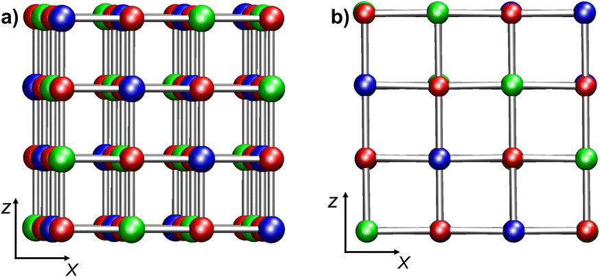 | ||
| Fig. 1 Ball-and-stick representations of (a) bulk NiO and (b) NiO(100) projected on the xz plane. (a) Model Bulk 1 (Ni32O32); (b) model RegSurf 1 (Ni32O32). Color codes: red, O; blue, Ni (spin-up); green, Ni (spin-down). | ||
Typically, in NiO materials, the conduction band (CB) arises from Ni 3d-states, whereas the valence band (VB) is dominated by O 2p-states’ contribution.10 The wide range of experimentally reported Egap values (3.2–4.3 eV)10,12–14 for NiO systems obtained through different synthetic routes14,15 can be traced back to the different structural organization (bulk single crystal, nanostructured films, nanoparticles,…),16 as well as to the presence of various defects.17,18 Band gaps for NiO nanomaterials/thin films11,12,19,20 are generally lower than the homologous values measured for bulk NiO10,21 and fall close to the Vis spectral region, paving the way to eventual end uses in sunlight-powered systems, such as solar cells and photocatalysts.17,22,23 The electronic properties of bulk NiO have been extensively investigated10–12,19,21,24–26 in relation to the origin of its semiconducting behaviour, arising from two competitive mechanisms (d–d transitions and charge transfer from O 2p-states to Ni d-states).10 Nonetheless, further studies are undoubtedly necessary in order to attain a deeper insight into the interplay between the structure and electronic properties for defective NiO films and nanostructures as a function of various parameters. For instance, Egap values in NiO thin films may significantly vary as a function of growth temperature,27,28 thickness,28 or annealing temperature.14 Furthermore, although NiO thin films typically feature a p-type character in the bulk phase,20 n- or p-type nickel(II) oxide systems can be fabricated by varying the oxygen partial pressure during the preparation processes.18 In addition, even the presence of defects can significantly influence the electronic properties of the resulting nanosystems.14,17,20,22
In this context, we recently focused on the chemical vapour deposition (CVD) of NiO using a series of closely related β-diketonate-diamine Ni(II) precursors.15,29,30 The system's chemico-physical characterization highlighted a significant effect exerted by water vapour in the reaction atmosphere on the resulting nanomaterial properties, with particular regard to the obtainment of (100)-oriented p-type films with Egap ≈ 3.40 eV.15,31 As a matter of fact, surface –OH groups were present on all samples as typically observed for thin films obtained through various fabrication routes.8,32–34 Nevertheless, the influence of such moieties on the structural and electronic properties of the fabricated nickel oxide nanomaterials has not been elucidated in detail, due also to the inherent experimental difficulties in achieving a molecular-level insight into the nature of the related defects.35–37 In particular, so far calculations were performed on the adsorption of water on NiO(100)38 and hydroxylated NiO(111) surfaces,39 but, to the best of our knowledge, theoretical investigations on NiO(100) surfaces bearing –OH groups have never been performed to date.
On this basis, the present work aims at shedding more light on this challenging issue, by investigating both regular (stoichiometric) and –OH-bearing NiO(100) surfaces via a theoretical approach based on density functional theory (DFT) and enhanced by a Hubbard Hamiltonian method. Such a strategy offers a valuable compromise between accuracy and computational cost, as it ensures a reasonable description of the NiO electronic structure,19,40 while providing the opportunity of simulating relatively extended material portions, bearing different kinds of –OH defects. Bulk NiO models, to be used as a reference for electronic properties, were also considered for comparison purposes. The choice of the (100) orientation was set based on the characterization of our NiO thin films (see above) and other previous studies of NiO nanomaterials obtained using different synthetic methods.3,41–48 As a matter of fact, the (100) surface is the least polar among NiO ones, being characterized by an equal number of O and Ni ions (Fig. 1b). In addition, (100) facets bear an equal number of spin-up and spin-down Ni cations, allowing for an even perturbation of the two magnetic sub-lattices through the introduction of surface defects.20 To explore the effect of different types of –OH defects, several defective NiO(100) models were taken into account, simulating, e.g. the presence of –OH groups either on O or Ni atoms of the outermost layer, or the dissociative chemisorption of water molecules on NiO(100) surfaces, and the effect of increasing –OH coverage. A detailed analysis of the structure and electronic properties of the regular and –OH-containing NiO(100) model systems was performed, with the aim of investigating atomic-level relationships between the different structures/types of –OH defects exhibited by the surface and the system electronic structure. The most relevant results are presented herein and critically discussed.
Models and calculations
Bulk NiO has a cubic rock-salt structure with a crystallographic cell parameter of 4.173 Å.10 Each Ni is coordinated by six O atoms in an octahedral environment. The cubic crystallographic unit cell contains four Ni and four O atoms. Due to the AF ordering, the magnetic unit cell parameter is twice as large as the crystallographic unit cell one. Consequently, the cubic magnetic unit cell corresponds to a 2 × 2 × 2 crystallographic unit cell (Ni32O32, Fig. 1a). A tetragonal 2 × 2 magnetic unit cell can also be defined (Ni16O16) (ESI section S1.1†).Calculations on bulk NiO were performed on three models: Bulk 1 (Ni32O32, cubic simulation cell, Fig. 1a), Bulk 2 (Ni64O64, orthorhombic simulation cell, obtained by doubling the magnetic cubic cell along the x direction), and Bulk 3 (Ni16O16, tetragonal 2 × 2 simulation cell) (ESI section S1.1 and Fig. S1†). With regard to NiO(100) surfaces, both regular and defected slab models were considered (ESI sections S1.2 and S1.3†). A vacuum region of 14 Å in the z direction was included with the aim of minimizing inter-slab interactions. Convergence with respect to vacuum gap size was confirmed by test calculations with a 17 Å vacuum (ESI, section S4, Table S1 and Fig. S11†). For regular NiO(100), the following two models were set up: RegSurf 1 (Ni32O32, Fig. 1b) and RegSurf 2 (Ni64O64, Fig. S2b†), exhibiting 8 and 16 top-layer Ni atoms, respectively. Both models are constituted by four NiO layers (see ESI section S1.2 and Fig. S2†). Modeling of defective NiO(100) surfaces requires particular attention due to NiO AF ordering.20,49 Since NiO is constituted by two symmetric spin-up and spin-down magnetic sub-lattices, the presence of a single defect – for example, an –OH group on a Ni atom of the outermost layer – will break the symmetry between the two sub-lattices, leading to uneven perturbations of the AF ordering.20,49 This case was investigated by considering three models of different sizes: Ni32O32(OH), Ni16O16(OH), and Ni24O24(OH) (see ESI section S1.3.1, Fig. S3†). While the first two models exhibit four layers, the latter contains six NiO layers, in order to assess the convergence with respect to slab thickness (ESI section S4, Table S1 and Fig. S11†).
All the other –OH containing NiO(100) models were built by including adsorbed groups in pairs, in order to evenly perturb the two spin sub-lattices.20 Hydroxyl groups on top of NiO(100) can be obtained in two ways, i.e. by adding either an –H atom to an O site or an –OH group to a Ni site of the NiO(100) top-layer. In all these models, an equal number of H atoms or OH groups were added to each magnetic sub-lattice, and their location was set so as to maximize the distance between defects (see ESI sections S1.3.2 and S1.3.3†).
The influence of two top-layer hydroxyls per NiO(100) simulation cell was studied on models of different surface areas, with the aim of exploring the effects of increasing defect concentration. To mimic surfaces characterized by a low –OH coverage, four different models were considered using the largest regular slab, namely RegSurf 2 (Ni64O64), containing 16 Ni surface sites (ESI section S1.3.2, Fig. S4†). In a different way, a higher –OH surface density was mimicked by slabs built from the tetragonal 2 × 2 cell and characterized by 4 Ni surface sites (ESI section S1.3.2, Fig. S5†).
The effect of the presence of four –OH groups was also studied on models with different surface areas. Specifically, a model characterized by lower –OH concentration was built from RegSurf 2, whereas high –OH coverage of the NiO(100) surface was simulated using three slab models built from the tetragonal 2 × 2 cell (ESI section S1.3.3, Fig. S6†).
Ultra-soft pseudopotentials50,51 were employed for Ni, O and H atoms, with the (spin polarized) PBE52 approximation to DFT employed for geometry optimization, which provides a reliable description of metal oxide structural properties.37,53,54 Corrections to dispersion interactions were included by using the D3-bj empirical model.55 The valence electrons adopted for each species are: Ni 3s23p63d84s2; O 2s22p4; and H 1s1. Electronic states were expanded in plane waves up to a 60 Ry cutoff (320 Ry for the electron density). Band gaps and magnetization were calculated on the optimized structures via the DFT+U approach by incorporating a Hubbard U term into the Hamiltonian.56 The adopted U term is 6.4 eV, a value in line with literature data.40 In the optimization procedure, the starting spin polarizations of the two kinds of Ni were given opposite signs. The total and absolute magnetization were calculated self-consistently, which is an appropriate procedure for magnetic oxide systems.57–59 The electronic structure type of each system (i.e., p-type, n-type, metal, and semimetal) was determined from the pertaining density of states (DOS) by comparing the energies of the VB and CB band edges with the Fermi level,60,61 conventionally set to 0. Calculations were performed with the Quantum ESPRESSO code.62 Further details on the electronic structure calculations are reported in ESI section S1.4.†
Results and discussion
Bulk NiO
Bulk NiO has been the subject of many theoretical calculations.10–12,19,21,24–26,49 Since the focus of this study is the effect of –OH defects on NiO(100) surfaces, the properties calculated for our bulk models (specifically, optical band gap, magnetic moments, and density/partial density of electronic states) should be considered as reference data, which will be compared with the values calculated for the slab models with the same computational setup.The calculated lattice parameter for bulk NiO (a = 4.175 Å), obtained from full structural optimization, reproduced very well the experimental value (4.173 Å).10 The three bulk models presented identical structural features and very similar electronic and magnetic properties (see Table 1). Each Ni atom is surrounded by six O atoms at a distance of 2.086 Å. The total magnetization of the system (μtot) equals 0.00 Bohr magnetons (μB), in line with the experimentally detected AF ordering. The absolute magnetization per Ni atom (μNi) is comparable with the reported experimental values (1.64–1.77μB).10,21 The calculated Egap (Table 1) is smaller than the quoted Egap values for bulk NiO systems (4.0–4.3eV)10,21,25,26,63 due to the known limitations of DFT and even DFT+U approaches leading to Egap underestimation,19,40,49,56 in particular for NiO-based materials.12 Nonetheless, the Egap, magnetization and lattice parameters are in line with the results obtained in other DFT+U studies on bulk NiO.19 The investigated bulk systems reproduced the experimentally detected p-type behavior, as can be deduced from the total electronic density of states (DOS) (see Fig. 2a). The DOS for the three bulk models are very similar (ESI section S2, Fig. S7†), in line with the corresponding Egap values (Table 1).
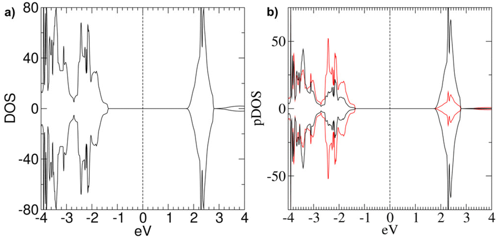 | ||
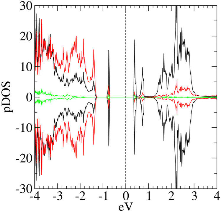
| Fig. 2 (a) DOS and (b) pDOS calculated for Bulk 1 (Ni32O32). The vertical dashed line represents the position of the Fermi level, conventionally set to 0. Positive curves: spin-up components; negative curves: spin-down components. Black and red lines in (b) refer to Ni d-states and O 2p-states. | ||
| System | E gap | E VB | E CB | Type | μ tot | μ Ni | d(Ni–O) | d(Ni–Ni) |
|---|---|---|---|---|---|---|---|---|
| Bulk | ||||||||
| Bulk 1 (Ni32O32) | 3.030 | −1.531 | +1.679 | p | 0 | 1.77 | 2.086 | 2.951 |
| Bulk 2 (Ni64O64) | 3.030 | −1.334 | +1.696 | p | 0 | 1.77 | 2.086 | 2.951 |
| Bulk 3 (Ni16O16) | 2.980 | −1.303 | +1.677 | p | 0 | 1.80 | 2.086 | 2.951 |
| Slab | ||||||||
| RegSurf 1 (Ni32O32) | 2.165 | −0.656 | +1.509 | p | 0 | 1.82 | 2.073/2.101 | 2.951 |
| RegSurf 2 (Ni64O64) | 2.195 | −1.054 | +1.121 | p | 0 | 1.82 | 2.080/2.092 | 2.951 |
The partial DOS (pDOS) calculated for Bulk 1 (Fig. 2b) indicate a dominant contribution of O 2p-states at the top of the VB, whereas at the bottom of the CB there is a higher density of empty Ni d-states. This finding is in line with literature data on NiO materials.10,21,25,26 Furthermore, the pDOS of occupied d-states at the top of the VB is not negligible, suggesting that even Ni d–d transitions might be relevant for the overall electronic properties of bulk NiO.26
Regular NiO films
The structures of the two regular slabs (Fig. 1b and ESI Fig. S2†) present some common features. The top layer exhibits a modest corrugation: O atoms are slightly displaced inwards (2.030 Å from the nearest Ni in the second layer), whereas Ni atoms are slightly displaced outward (2.090 Å from the nearest O in the second layer). For comparison, the Ni–O bond distances in the bulk system are 2.086 Å. Even Ni–O distances in the top layer are different: they form chains of alternating short (2.073 Å) and long (2.101 Å) bonds (Table 1). The surface relaxation affects mostly the two top layers (ESI section S3†), in line with the results of scanning tunnelling microscopy (STM) experiments on NiO surfaces.64The AF ordering is maintained in stoichiometric (100) slabs, whereas μNi increases slightly with respect to the corresponding bulk value (Table 1).
The Egap values calculated for regular NiO(100) surfaces are reported in Table 1, indicating a substantial decrease in comparison with that of the bulk structure, in line with the Egap trend expected from previous data.11,12,19,20 This phenomenon can be attributed to the above-discussed surface deformations. Both slabs have p-type character, and their pDOS (Fig. 3 and Fig. S9†) indicate a predominance of O 2p-states, and minor contributions from occupied Ni d-states at the VB top. The similarities between the pDOS pertaining to regular slab and bulk models suggest that the main electronic structure features of bulk NiO are maintained in regular NiO(100) films.
 | ||
| Fig. 3 pDOS calculated for RegSurf 2 (Ni64O64). The vertical dashed line represents the position of the Fermi level, conventionally set to 0. Positive curves: spin-up components; negative curves: spin-down components. Black and red lines refer to Ni d-states and O 2p-states, respectively. | ||
Hydroxylated NiO(100) films
Each layer of the regular NiO(100) surfaces contains parallel rows of spin-up or spin-down Ni cations along the (111) planes (Fig. 1). Hence, each top-layer oxygen atom has two spin-up and two spin-down Ni cations as nearest-neighbors on opposite sides (see Scheme 1). In addition, the oxygen atoms of the top layer are located above either spin-up or spin-down Ni cations of the layer below. Therefore, the formation of a surface –OH group by addition of an H atom to an O site (Scheme 1a) or by binding of an –OH group to a Ni center (Scheme 1b) leads to the breaking of the pristine magnetic symmetry.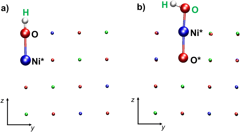 | ||
| Scheme 1 Schematic representations of: (a) an –OH defect formed by binding an H atom to a top-layer oxygen; (b) an –OH defect formed by binding a hydroxyl group to a top layer Ni atom. Atoms directly involved in the defect are highlighted as spheres. Color codes: red, O; blue, Ni (spin-up); green, Ni (spin-down). The (a) H and (b) OH atoms adsorbed on the NiO(100) surface are labeled in green; Ni*: Ni atom bearing the –OH group; O*: O atom bonded to Ni*. | ||
In the case of mono-hydroxylated models (see ESI section S4, Table S1 and Fig. S11†), the system becomes half-metallic since the presence of –OH on a single Ni site unevenly perturbs the slab AF ordering. Such a result is also in line with previous literature data.65
Hence, in all the other models herein considered, the –H and –OH moieties were added in pairs and their relative positions were set so as to preserve the magnetic symmetry of the spin-up and spin-down sub-lattices.
The effect of increasing the concentration of surface hydroxyl defects was investigated using models including either two or four hydroxyls per slab, as described below. In each case, slabs with surface areas of 34.86 Å2 and 8.72 Å2 were adopted to model low and high surface densities of defects, respectively.
[Ni64O64]2H. In the optimized structure of this model (Fig. 4a), the top layer corrugation is more pronounced with respect to the regular slab. The OH groups, nearly perpendicular to the (100) plane, are separated by 9.168 Å (Table 2). The distance of the OH oxygen from Ni* is 2.905 Å, indicating that these oxygen atoms are ≈0.7 Å outward from the top layer. The AF structure is preserved even in this model (μtot = 0.00μB), whereas μNi is 1.78μB. The addition of two H atoms severely modifies the electronic structure with respect to regular NiO(100) surfaces (Table 2 and Fig. 5a).
 | ||
| Fig. 4 Ball-and-stick representation (projected on the xz plane) of di-hydroxylated NiO(100) model slabs mimicking a low concentration of surface hydroxyl groups. (a) [Ni64O64]2H, containing two H, each bonded to an O atom of the top layer; (b)[Ni64O64]2(OH), containing two neutral –OH defects bonded to Ni atoms with opposite spin. Color codes: red, O; blue, Ni (spin-up); green, Ni (spin-down); white, H. | ||
 | ||
| Fig. 5 pDOS computed for defective slab models: (a) [Ni64O64]2H; (b) [Ni64O64]2(OH). The vertical dashed line at 0 eV represents the Fermi level position. Positive curves: spin-up components; negative curves: spin down components. (a) Black lines: Ni d-states; red lines: O 2p-states; green lines: hydroxyl O 2p-states; (b) black lines: Ni d-states; red lines: O 2p-states; green lines: Ni* d-states; blue lines: hydroxyl O 2p-states. | ||
| System | E gap | E VB | E CB | E intra-gap | Type | μ tot | μ Ni | d(OH–OH) |
|---|---|---|---|---|---|---|---|---|
| 2 –OH groups | ||||||||
| [Ni64O64]2H | 0.682 (1.86) | −1.637 | +0.222 | −1.36; −1.17; −0.46 | n | 0 | 1.78 | 9.168 |
| [Ni64O64]2(OH) | 0.250 (2.11) | −0.229 | +1.881 | +0.021 | p | 0 | 1.80 | 9.157 |
| [Ni24O24]2H | 1.100 (1.59) | −1.238 | +0.352 | +0.748 | n | 0 | 1.79 | 4.173 |
| [Ni24O24]2(OH)a | 0 | Metal | 0 | 1.82 | 2.951 | |||
| [Ni24O24]2(OH)b | 0 | Metal | 0 | 1.70 | 4.171 | |||
| 4 –OH groups | ||||||||
| [Ni64O64]2H-2(OH) | 1.225 (2.01) | −0.929 | +1.085 | −0.43; −0.30; −0.14 | p | 0 | 1.80 | 4.974/9.195 |
| [Ni24O24]4H | 1.330 | −0.715 | +0.615 | — | p | 0 | 1.70 | 2.879/4.176 |
| [Ni24O24]4(OH) | 0 | Metal | 0 | 1.74 | 2.911/4.281 | |||
| [Ni24O24]2H-2(OH) | 2.100 | −0.448 | +1.652 | — | p | 0 | 1.81 | 4.127 |
Specifically, the main changes detected in the electronic properties are a drastic Egap decrease (0.682 eV), the appearance of donor states in the gap, and the change from p-type to n-type character (Fig. 5a), as indicated by the relative positioning of the Fermi Level in the [Ni64O64]2H pDOS. As already highlighted, changes from p-type to n-type have been reported for NiO thin films by varying the oxidative conditions in the film preparation.18 Interestingly, the pDOS indicates substantial Ni participation in the donor states in the gap (Fig. 5a).
To attain an insight into electrically charged OH defects, we also evaluated the effects of diluted H+ on top of the [Ni64O64] regular slab (see ESI section S5.1.3 and Fig. S12a†). The main difference compared to the neutral [Ni64O64]2H system lies in the electronic structure. In particular, the charged model ([Ni64O64]2H+) has no states in the gap and a p-type behaviour (ESI, Table S2†).
[Ni64O64]2(OH). The minimum energy structure of this model is illustrated in Fig. 4b. Even in this case, the top layer is corrugated, with Ni atoms positioned slightly upward (≈0.1 Å) with respect to oxygen atoms. However, the surface deformation induced by the binding of two hydroxyls to Ni* is less pronounced than that caused by the addition of two H atoms to two surface O sites (cfr. Fig. 4a and b). Nonetheless, the two slabs have very similar magnetization values (Table 2).
Empty states are present in the gap (Table 2), thus narrowing Egap from 2.11 eV (i.e., the energy difference between the bottom CB and the top VB, ECB − EVB) to 0.250 eV (i.e., the energy difference between the lowest empty state and the highest occupied state). The model system has a p-type behavior (Fig. 5b), and both Ni* and hydroxyl O atoms directly contribute to the empty state in the gap, located very close to the Fermi Level (+0.021 eV). Additionally, there is a higher density of O 2p-states at the VB top. In a different way, the density of Ni d-states and O 2p-states at the CB bottom are similar, while, at higher energies, the Ni-d-states become predominant (Fig. 5b).
Even for this system, we examined the effects of two diluted charged OH defects on the [Ni64O64] slab (ESI section S5.1.4, Fig. S12b†). In short, the main difference between [Ni64O64]2(OH) and the negatively charged [Ni64O64]2(OHm) model lies in the intra-gap states. In the neutral system, such states are empty and located just below the Fermi level. Conversely, in the charged model, the excess electrons occupy these intra-gap states, thus increasing Egap (ESI Fig. S12b and Table S2†).
[Ni24O24]2H. The minimum energy structure (Fig. 6a and b) is characterized by parallel rows of –OH moieties, due to the high surface density of defects. The separation between –OH defects is nearly half that in the low-concentration model [Ni64O64]2H (Table 2). Indeed, each hydroxyl group is now surrounded by four –OH defects on Ni* sites with opposite spin (ESI section S5.2.1, Fig. S13†).
 | ||
| Fig. 6 Ball-and-stick representations of di-hydroxylated NiO(100) 6-layer model slabs built with the 2 × 2 tetragonal cell and mimicking a higher concentration of surface hydroxyl groups: (a) side view and (b) top view of [Ni24O24]2H, with two H, each bonded to an O atom of the top layer; (c) side view and (d) top view of [Ni24O24]2(OH)a, with two adsorbed –OH separated by 2.951 Å; (e) side view and (f) top view of [Ni24O24]2(OH)b, with two adsorbed –OH separated by 4.171 Å. The two –OH groups are bonded to Ni atoms with opposite spin. Color codes: red, O; blue, Ni (spin-up); green, Ni (spin-down); white, H; red dashed lines, hydrogen bonds. The blue solid lines represent the size of the simulation cell. | ||
Each –OH bridges two top-layer Ni* centers of opposite spins (Fig. 6b), with distances of 2.175 Å and 2.454 Å, respectively, whereas the separation of the hydroxyl oxygen from Ni* is 3.037 Å. A comparison of the local environment of the defects with the [Ni64O64]2H case (ESI section S5.2.1†) indicates that structural distortions with respect to regular NiO(100) become more pronounced with increasing defect density. Conversely, the magnetic properties and the main electronic structure features of the two models are very similar (Table 2). In particular, both models have n-type behavior and occupied states in the gap.
The [Ni64O64]2H pDOS (Fig. 7) evidence a major contribution of Ni d-states to the occupied state in the gap. Interestingly, the hydroxyl O atoms contribute both to the intra-gap states and to the CB bottom, whereas the VB top is mainly constituted by O 2p-states.
 | ||
| Fig. 7 pDOS computed for the slab model [Ni24O24]2H. The vertical line represents the Fermi level position. Positive curves: spin-up components; negative curves: spin down components; black lines: Ni d-states; red lines: oxygen 2p-states; green lines: hydroxyl O 2p-states. | ||
[Ni24O24]2(OH). In the optimized structures of the two [Ni24O24]2(OH) systems (i.e., [Ni24O24]2(OH)a and [Ni24O24]2(OH)b), the –OH groups are separated by 2.951 Å and 4.171 Å, respectively. In [Ni24O24]2(OH)a, each Ni*–OH group moved on top of two top-layer oxygen atoms, leaving an under-coordinated O atom in the layer below (see Fig. 6c and d). Each Ni* atom forms two strong bonds (1.888 Å) with the two neighboring top-layer oxygens, with an O–Ni*–O angle of 127.6°. The Ni*–OH distances are 1.784 Å, the O–H bond lengths are 0.990 Å, and the Ni*–O–H angles are 110.8°. These geometrical parameters clearly indicate that Ni* atoms are three-coordinated (Fig. 6c). The –OH groups are aligned along the y direction (Fig. 6c and d), forming hydrogen-bonded chains characterized by an O⋯HO separation of 2.050 Å, indicating the occurrence of moderately strong hydrogen bonds.
The [Ni24O24]2(OH)b system exhibits very different structural features (Fig. 6e and f). First of all, there is no massive reconstruction like in the [Ni24O24]2(OH)a model. The –OH groups are positioned on two top-layer Ni* atoms, which are moderately upward shifted (Fig. 6e). Specifically, the Ni*–O* distances (2.081 Å) are longer than the average Ni–O distance between top- and second-layer atoms (1.998 Å). The Ni*–OH distances are 1.801 Å, the O–H bonds are 0.981 Å, and the Ni*–O–H bond angles are 107.9°. In this case, due to the large separation between –OH groups (4.171 Å), no hydrogen bond is formed.
Although both systems have zero μtot, the μNi values are different (Table 2), likely due to the very different geometric structures.
The substantial difference in the top-layer structures results in largely different pDOS profiles, mainly above the Fermi level (ESI section S5.2.2, Fig. S14†). However, both models, characterized by a high density of surface –OH groups, have zero Egap, thus indicating metallic behaviour (Table 2). Such metallic behaviour is not predicted for [Ni64O64]2(OH), which has the same number of –OH groups, but it is characterized by a lower surface coverage (0.125 vs. 0.5) and a larger –OH group separation.
[Ni64O64]2H-2(OH). The minimum energy structure of this model is shown in Fig. 8, while the corresponding pDOS values are depicted in Fig. 9a. The two OH groups coordinated to top-layer Ni* atoms are separated by 9.195 Å, the same distance that separates the two H atoms bonded to top layer oxygens. The shortest separation between different types of OH species is much smaller (4.974 Å).
 | ||
| Fig. 8 Ball-and-stick representation of the model slab (Ni64O64)2H–2(OH) projected along the xz plane. The two –H groups are bonded to top layer oxygens, whereas the two –OH groups are bonded to Ni atoms with opposite spin. Color codes: red, O; blue, Ni (spin-up); green, Ni (spin-down); white. H. | ||
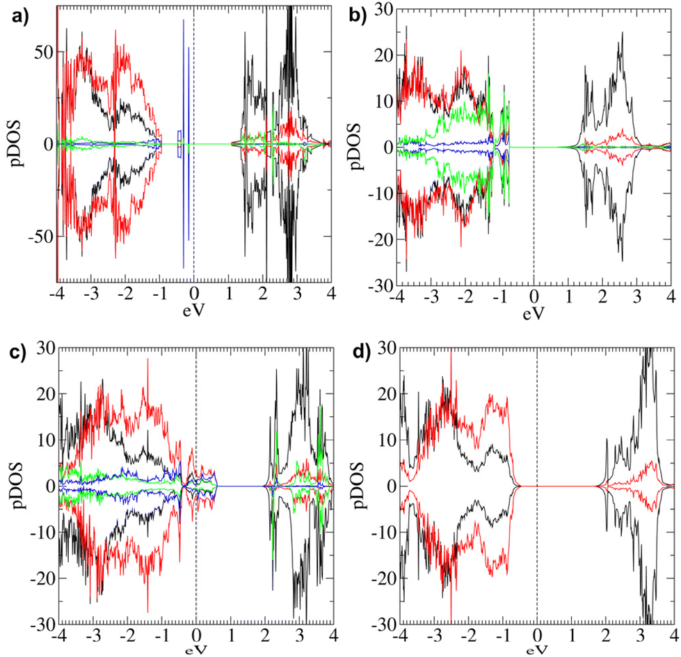 | ||
| Fig. 9 pDOS computed for models (a) [Ni64O64]2H-2(OH); (b) [Ni24O24]4H; (c) [Ni24O24]4(OH); (d) [Ni24O24]2H-2(OH). The vertical dashed line represents the Fermi level position. Positive curves: spin-up components; negative curves: spin down components; black lines: Ni d-states; red lines: O 2p-states; green lines: Ni* d-states; blue lines: hydroxyl O 2p-states. | ||
Even in this model, top layers are corrugated (ESI section S6.1.1†), with Ni atoms typically shifted upward with respect to O ones (except for the H-bearing oxygens). The AF ordering is maintained (Table 2). Concerning the electronic structure, this system is characterized by a p-type behavior. Egap is 1.225 eV, while ECB–EVB amounts to 2.01 eV (Table 2). Indeed, such a difference is due to the appearance of occupied electronic states between the top of the VB and the bottom of the CB, as highlighted by the corresponding pDOS (Fig. 9a). In particular, these states are located below the Fermi level (Table 2) and are mostly due to hydroxyl O atoms. The contribution of states belonging to oxygen atoms is predominant at the VB edge. In a different way, at the CB edge, Ni d-states and O 2p-states show a very similar contribution. Only at higher energy does the density of Ni d-states become much larger.
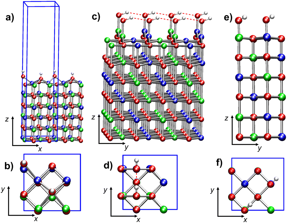
[Ni24O24]4H. The optimized structure of this model (Fig. 10a and b), very different from the initial optimization guess (ESI Fig. S6b†), evidences an important top layer reconstruction. Only two of the four Ni* are at bond distances (2.110 Å) from the O atoms of the second layer (Fig. 10a). These two Ni* cations (of opposite spin) are also bonded to two hydroxyl oxygens each, hence they are three-coordinated. The other two Ni* cations are tetra-coordinated by O atoms of the four –OH groups (Fig. 10b). Such tetra-coordinated Ni* cations are separated by 2.535 Å from the plane of the second layer and by 2.730 Å from the closest second-layer oxygen. This massive reconstruction, featuring both three- and tetra-coordinated Ni, is due to the displacement of the top layer with respect to the second layer by ≈0.898 Å in the [–110] direction (see the arrow in Fig. 10b). As found for the [Ni64O64]2H and [Ni24O24]2H systems, the O–H bonds are nearly parallel to the z-direction. Further structural details on this reconstructed surface can be found in ESI section S6.1.2, Fig. S15.†
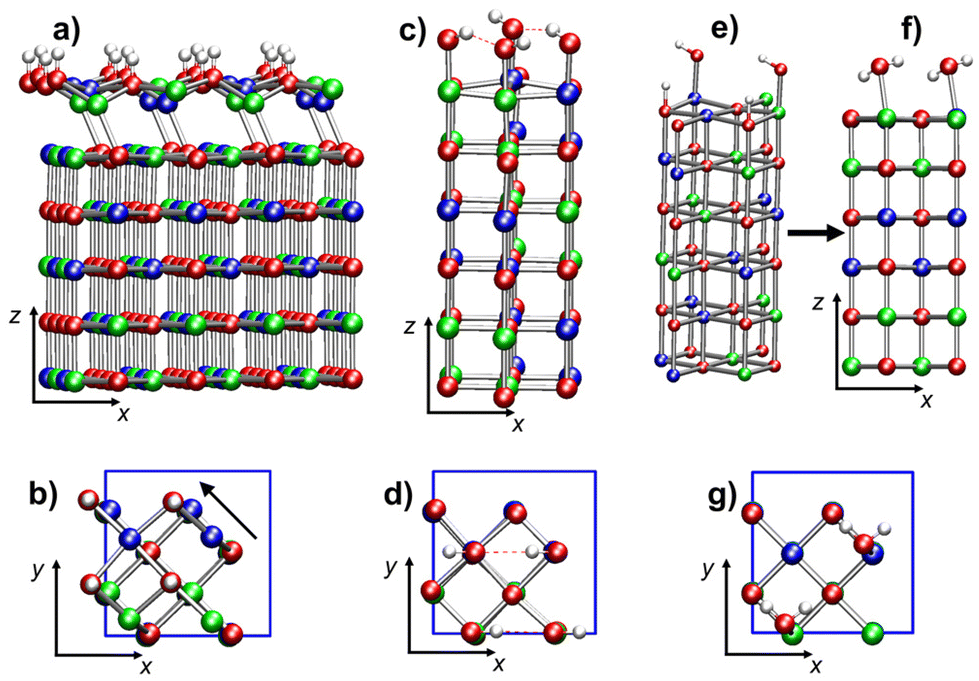 | ||
| Fig. 10 Ball-and-stick representations of tetra-hydroxylated NiO(100) 6-layer models built with the 2 × 2 tetragonal cell and mimicking a higher concentration of surface –OH groups: (a) side view and (b) top view of [Ni24O24]4H, with four H, each bonded to an O atom of the top layer; (c) side view and (d) top view of [Ni24O24]4(OH), with four –OH groups bonded to the four top-layer Ni atoms; (e) starting configuration (side view) of the [Ni24O24]2H-2(OH) model, mimicking two dissociated H2O molecules; (f) (side view) and (g) (top view) of the optimized geometry of [Ni24O24]2H-2(OH), featuring two molecularly adsorbed H2O molecules on top of NiO(100). Color codes: red, O; blue, Ni (spin-up); green, Ni (spin-down); white, H; red dashed lines, hydrogen bonds. | ||
In spite of the considerable structural relaxation with respect to regular NiO(100), this system maintains zero magnetization. However, μNi is lower than the bulk value (Table 2). Interestingly, the calculated electronic properties of this model (Table 2 and Fig. 9b) evidence a p-type behavior with no intra-gap states. Upon increasing the density of this kind of defect, a shift from n-type (in [Ni64O64]2H and [Ni24O24]2H) to p-type behavior (in [Ni24O24]4H) is observed, along with the increase of defect states at the top of the VB (see Fig. 5a, 7 and 9b).
[Ni24O24]4(OH). This system has a surface –OH density twice as large as that of [Ni24O24]2(OH), and eight times greater than that of [Ni64O64]2(OH). In this case, the slab minimum energy structure (Fig. 10c and d) does not present substantial distortions from the geometry of regular NiO(100) surfaces. The four –OH groups are bonded to the four top-layer Ni atoms. Each spin sub-lattice is characterized by the alternation of shorter and longer Ni*–OH distances—1.808 Å and 1.826 Å, respectively. All O–H bond lengths are 0.989 Å. The hydroxyl groups attached to spin-up and spin-down Ni* cations are aligned to the −x and +x directions, respectively, forming chains of moderately strong hydrogen bonds with alternating distances (2.015 Å and 2.089 Å). Even the Ni*–O–H bond angles occur in pairs in each hydrogen-bonded chain (107.9° and 107.0°).
The data in Table 2 indicate that the AF character is maintained in this model as well and that the system is metallic. Interestingly, the pDOS (Fig. 9c) highlights a significant contribution of the defect states at the Fermi Level, higher than the di-hydroxylated models (ESI, Fig. S14†), that can be ascribed to the higher density of this kind of defect.
[Ni24O24]2H-2(OH). This last model is the result of the optimization of a system built by placing two –H and two –OH moieties on two top-layer O and Ni centers, respectively (Fig. 10e), thus mimicking two adsorbed dissociated water molecules, at a much higher concentration (8 times greater) than in the [Ni64O64]2H-2(OH) model slab. After optimization, the system evolved toward the formation of two water molecules physisorbed on two Ni atoms with opposite spin (Fig. 10f and g). The arrangement of the water molecules in the final optimized structure closely resembles the geometry found for hydrated NiO(100) at 0.5 monolayer coverage.38 The separation between H2O oxygen atoms is 4.127 Å, and water protons are not involved in hydrogen bonds with surface oxygens. The geometry of the adsorbed water molecules is in line with previously reported data:38 the O–H bond distances are 0.980 Å and 1.000 Å, and the H–O–H bond angle is 104.2°. With respect to the local environment of the water molecules, the Ni*–Owater separation is 2.216 Å, whereas the distance of Ni* from the closest second-layer O atom (O*) is 2.110 Å, and the O*–Ni*–Owater angle is 167.1°.
The system has zero total magnetization and a μNi of 1.81μB. A p-type behaviour is found, with an Egap of 2.10 eV (Table 2 and Fig. 9d). These results suggest that the electronic properties of NiO(100) are only moderately affected by the physisorption of water molecules, even at high coverage.
Discussion
In the slab models, the hydroxyl defects were introduced either by adding H atoms on top layer oxygen atoms and/or by adding OH groups to top layer Ni atoms (Scheme 1). Moreover, using models with different surface areas, we have explored different coverage regimes.When chemisorbed defects are introduced in pairs so as to evenly affect the two spin sub-lattices, the surfaces are characterized by AF ordering, like the bulk phase. The calculated gap values decrease on passing from the bulk to the slab models, in line with experimental results reporting a smaller Egap for NiO films with respect to the bulk counterpart.11,12,19,20 Moreover, our calculations predict that the presence of OH groups reduces the Egap with respect to the regular (100) slabs.
The electronic properties of defective slabs depend on how the –OH groups are bonded to the surface. Indeed, a different behavior as a function of coverage is found when the –OH groups are formed by linking H atoms to oxygen atoms in the topmost layer (Scheme 1a) or by linking –OH groups to surface Ni sites (Scheme 1b).
In passing from [Ni64O64]2H to [Ni24O24]4H, the increase in the density of surface defects brings about a decrease of the number of intra-gap states, a shift from n-type to p-type behavior, and an increase of Egap (Table 2). Conversely, on passing from [Ni64O64]2(OH) to [Ni24O24]4(OH), a decrease of Egap is observed, leading to metallic behavior at a high –OH concentration.
From the structural point of view, we have detected two different NiO(100) surface reconstructions at a high defect density, for the [Ni24O24]2(OH)a and [Ni24O24]4H models. In both cases, three-coordinated Ni centers are formed. For [Ni24O24]4H, the reconstruction also leads to the formation of tetra-coordinated Ni, the disappearance of intra-gap states and a transition from an n-type to a p-type behavior.
The effect of introducing charged defects at low coverage has also been explored. The addition of H+ in comparison with the adsorption of neutral H atoms brings about a relevant change in the electronic structure of the system, leading to the disappearance of intra-gap states and a band gap increase. A similar effect on the electronic structure, with a significant Egap increase, is obtained for the binding of negatively charged OH− groups in comparison with neutral –OH moieties.
As a further insight, we have investigated the effect of the simultaneous addition of –H and –OH groups to top-layer O and Ni sites, respectively, in both low- and high-coverage regimes. Regarding the low-density case ([Ni64O64]2H-2(OH)), the electronic behavior seems to be due to a combination of the properties exhibited by the charged [Ni64O64]2H+ and [Ni64O64]2(OHm) slabs. Indeed, our calculations predict an Egap of 1.225 eV, i.e. an intermediate value between the [Ni64O64]2H+ and the [Ni64O64]2(OHm) cases, with p-type character and donor states below the Fermi level. The latter are mostly localized on the O atoms of surface hydroxyl groups (Fig. 9a). Among the considered –OH-bearing NiO(100) slabs, this system might be the model that approximates more closely NiO thin films fabricated via CVD under humid conditions.15
At higher coverage ([Ni24O24]2H-2(OH)), such kinds of defects are unstable, leading to the formation of molecularly adsorbed water that does not alter the p-type character of the surface.
Conclusions
In this work, we have presented an original comprehensive DFT study on NiO(100) surfaces characterized by the presence of –OH defects. Our results indicate that the antiferromagnetic ordering, typical of rock-salt bulk NiO, is maintained in the model slabs. The calculated band gap values decrease on passing from the bulk phase to (100) slabs, and such a reduction is enhanced by the presence of –OH defects. In this regard, the hydroxyl defects formed by linking H atoms to topmost layer oxygen atoms (Scheme 1a) or by attaching OH groups to Ni sites (Scheme 1b) lead to different modifications of the NiO(100) electronic structure. Specifically, we have shown that the chemical nature of the defects, as well as their concentration, plays a fundamental role in the electronic properties of the system, directly affecting the ultimate p-type or n-type character. In a different way, the presence of a single defect, affecting only one of the two magnetic NiO sub-lattices, results in a half-metallic electronic structure.An important outcome of the present investigation is the simulation of two new different reconstructed NiO(100) surfaces, induced at high coverages by the two kinds of defects considered herein, namely H adsorbed on O sites (Scheme 1a) and –OH adsorbed on Ni sites (Scheme 1b). In spite of the different structures of the reconstructed surfaces, both systems are characterized by three-coordinated Ni sites on the top layer and, in one case ([Ni24O24]4H), even by tetra-coordinated Ni(OH)4 moieties, leading to a plane of under-coordinated Ni sites.
Apart from these reconstruction cases, the presence of –H and/or –OH defects induces a corrugation of the top layers with an upward shift of the Ni atoms, which may alter the reactivity of NiO(100) surfaces in many processes of relevance for technological applications, such as gas sensing or heterogeneous catalysis.
Moreover, this study reveals that NiO(100) surfaces bearing both kinds of –OH defects at a high density are unstable and evolve towards the formation of molecularly adsorbed water.
In conclusion, the microscopic-level insight gathered herein from the theoretical study of –OH defects on NiO(100) models may help the understanding of the structural and electronic properties of NiO-based thin films of practical interest for a variety of eventual technological end uses.
Author contributions
All authors have contributed to the planning of the work, the setup of the models and data analyses. Calculations were performed at the computational facilities of Insubria University. All authors have contributed to the design and the writing of the manuscript.Data availability
The data supporting this article have been included as part of the ESI.†Conflicts of interest
There are no conflicts to declare.Acknowledgements
This work has received funding from Insubria University (FAR2022), from the National Council of Research (Progetti di Ricerca @CNR-avviso 2020-ASSIST), and from Padova University (P-DiSC#02BIRD2023-UNIPD RIGENERA, DOR 2021–2024).References
- X. Su, Z. Tu, L. Ji, H. Wu, H. Xu and C. Liu, J. Vac. Sci. Technol., A, 2023, 41, 062407 CrossRef.
- T. Moriyama, K. Oda, T. Ohkochi, M. Kimata and T. Ono, Sci. Rep., 2018, 8, 14167 CrossRef PubMed.
- R. L. Wilson, T. J. Macdonald, C.-T. Lin, S. Xu, A. Taylor, C. E. Knapp, S. Guldin, M. A. McLachlan, C. J. Carmalt and C. S. Blackman, RSC Adv., 2021, 11, 22199–22205 RSC.
- Q.-S. Jiang, Y. Wu, Z. Xie, M. Wei, Y. Zhao, X. Yang, W. Xun, S. Cao and C. Wang, Mater. Today Commun., 2023, 35, 106401 CrossRef.
- K. Rajesh, N. Pothukanuri and M. V. R. Reddy, Chem. Phys. Impact, 2024, 8, 100397 CrossRef.
- S. Srivastava, C. Dwivedi, A. Yadav, A. Kumar, G. Gupta and P. Singh, Mater. Lett., 2023, 351, 135040 CrossRef.
- D. Zywitzki, D. H. Taffa, L. Lamkowski, M. Winter, D. Rogalla, M. Wark and A. Devi, Inorg. Chem., 2020, 59, 10059–10070 CrossRef PubMed.
- N. Weidler, J. Schuch, F. Knaus, P. Stenner, S. Hoch, A. Maljusch, R. Schäfer, B. Kaiser and W. Jaegermann, J. Phys. Chem. C, 2017, 121, 6455–6463 CrossRef.
- K. Munawar, M. A. Mansoor, R. Naeem, M. Rizwan, M. S. Ahmad, T. Zaharinie, M. N. M. Zubir and Z. Aspanut, Thin Solid Films, 2023, 782, 140031 CrossRef.
- G. A. Sawatzky and J. W. Allen, Phys. Rev. Lett., 1984, 53, 2339–2342 CrossRef.
- J. Zaanen, G. A. Sawatzky and J. W. Allen, Phys. Rev. Lett., 1985, 55, 418–421 CrossRef.
- C.-Y. Kuo, T. Haupricht, J. Weinen, H. Wu, K.-D. Tsuei, M. W. Haverkort, A. Tanaka and L. H. Tjeng, Eur. Phys. J.:Spec. Top., 2017, 226, 2445–2456 Search PubMed.
- C. Park, J. Kim, K. Lee, S. K. Oh, H. J. Kang and N. S. Park, Appl. Sci. Converg. Technol., 2015, 24, 72–76 CrossRef.
- Y. R. Denny, K. Lee, C. Park, S. K. Oh, H. J. Kang, D.-S. Yang and S. Seo, Thin Solid Films, 2015, 591, 255–260 CrossRef.
- M. Benedet, C. Maccato, G. Pagot, C. Invernizzi, C. Sada, V. Di Noto, G. A. Rizzi, E. Fois, G. Tabacchi and D. Barreca, J. Phys. Chem. C, 2023, 127, 22304–22314 CrossRef.
- P. Alastuey, D. Pais Ospina, D. Comedi, M. Tirado and O. Marin-Ramirez, J. Am. Ceram. Soc., 2024, 107, 92–106 CrossRef.
- W. Chen, F.-Z. Liu, X.-Y. Feng, A. B. Djurišić, W. K. Chan and Z.-B. He, Adv. Energy Mater., 2017, 7, 1700722 CrossRef.
- M. I. Pintor-Monroy, B. L. Murillo-Borjas, M. Catalano and M. A. Quevedo-Lopez, ACS Appl. Mater. Interfaces, 2019, 11, 27048–27056 CrossRef.
- A. Rohrbach, J. Hafner and G. Kresse, Phys. Rev. B:Condens. Matter Mater. Phys., 2004, 69, 075413 CrossRef.
- K. O. Egbo, C. P. Liu, C. E. Ekuma and K. M. Yu, J. Appl. Phys., 2020, 128, 135705 CrossRef.
- B. E. F. Fender, A. J. Jacobson and F. A. Wedgwood, J. Chem. Phys., 1968, 48, 990–994 CrossRef.
- W. Chen, Y. Wu, J. Fan, A. B. Djurišić, F. Liu, H. W. Tam, A. Ng, C. Surya, W. K. Chan, D. Wang and Z.-B. He, Adv. Energy Mater., 2018, 8, 1703519 CrossRef.
- K. P. Makhado, M. M. Mphahlele-Makgwane, N. Kumar, P. G. L. Baker and P. R. Makgwane, Mater. Today Sustain., 2024, 25, 100664 Search PubMed.
- J. A. Dawson, Y. Guo and J. Robertson, Appl. Phys. Lett., 2015, 107, 122110 CrossRef.
- A. K. Cheetham and D. A. O. Hope, Phys. Rev. B:Condens. Matter Mater. Phys., 1983, 27, 6964–6967 CrossRef.
- A. Fujimori and F. Minami, Phys. Rev. B:Condens. Matter Mater. Phys., 1984, 30, 957–971 CrossRef.
- A. Boukhachem, R. Boughalmi, M. Karyaoui, A. Mhamdi, R. Chtourou, K. Boubaker and M. Amlouk, Mater. Sci. Eng., B, 2014, 188, 72–77 CrossRef.
- S. A. Mahmoud, A. Shereen and M. A. Tarawnh, J. Mod. Phys., 2011, 2, 1178–1186 CrossRef.
- M. Benedet, D. Barreca, E. Fois, R. Seraglia, G. Tabacchi, M. Roverso, G. Pagot, C. Invernizzi, A. Gasparotto, A. A. Heidecker, A. Pöthig, E. Callone, S. Dirè, S. Bogialli, V. D. Noto and C. Maccato, Dalton Trans., 2023, 52, 10677–10688 RSC.
- C. Invernizzi, G. Tabacchi, R. Seraglia, M. Benedet, M. Roverso, C. Maccato, S. Bogialli, D. Barreca and E. Fois, Molecules, 2024, 29, 642 CrossRef PubMed.
- G. Pagot, M. Benedet, C. Maccato, D. Barreca and V. Di Noto, Surf. Sci. Spectra, 2023, 30, 024028 CrossRef.
- K. Hemmati, A. Kumar, A. R. Jadhav, O. Moradlou, A. Z. Moshfegh and H. Lee, ACS Catal., 2023, 13, 5516–5528 CrossRef.
- D. Barreca, G. Carraro, E. Fois, A. Gasparotto, F. Gri, R. Seraglia, M. Wilken, A. Venzo, A. Devi, G. Tabacchi and C. Maccato, J. Phys. Chem. C, 2018, 122, 1367–1375 CrossRef.
- B. P. Payne, M. C. Biesinger and N. S. McIntyre, J. Electron Spectrosc., 2009, 175, 55–65 CrossRef.
- E. Fois, G. Tabacchi, D. Barreca, A. Gasparotto and E. Tondello, Angew. Chem., Int. Ed., 2010, 49, 1944–1948 CrossRef PubMed.
- G. Tabacchi, E. Fois, D. Barreca and A. Gasparotto, Int. J. Quantum Chem., 2014, 114, 1–7 CrossRef.
- D. Barreca, E. Fois, A. Gasparotto, C. Maccato, M. Oriani and G. Tabacchi, Molecules, 2021, 26, 1988 CrossRef PubMed.
- N. Yu, W.-B. Zhang, N. Wang, Y.-F. Wang and B.-Y. Tang, J. Phys. Chem. C, 2008, 112, 452–457 CrossRef.
- L. Li and Y. Kanai, Phys. Rev. B:Condens. Matter Mater. Phys., 2015, 91, 235304 CrossRef.
- M. Nolan, R. Long, N. J. English and D. A. Mooney, J. Chem. Phys., 2011, 134, 224703 CrossRef PubMed.
- M. Chandrakala, S. Raj Bharath, T. Maiyalagan and S. Arockiasamy, Mater. Chem. Phys., 2017, 201, 344–353 CrossRef.
- J.-K. Kang and S.-W. Rhee, Thin Solid Films, 2001, 391, 57–61 CrossRef.
- M. Utriainen, M. Kröger-Laukkanen and L. Niinistö, Mater. Sci. Eng., B, 1998, 54, 98–103 CrossRef.
- S. Elmassi, A. Narjis, L. Nkhaili, A. Elkissani, L. Amiri, S. Drissi, A. Abali, M. Bousseta and A. Outzourhit, Phys. B, 2022, 639, 413980 CrossRef.
- A. A. Ahmed, N. Afzal, M. Devarajan and S. Subramani, Mater. Res. Express, 2016, 3, 116405 CrossRef.
- H.-W. Ryu, G.-P. Choi, G.-J. Hong and J.-S. Park, Jpn. J. Appl. Phys., 2004, 43, 5524 CrossRef CAS.
- M. S. Jamal, S. A. Shahahmadi, P. Chelvanathan, H. F. Alharbi, M. R. Karim, M. Ahmad Dar, M. Luqman, N. H. Alharthi, Y. S. Al-Harthi, M. Aminuzzaman, N. Asim, K. Sopian, S. K. Tiong, N. Amin and Md. Akhtaruzzaman, Res. Phys., 2019, 14, 102360 Search PubMed.
- J. M. McKay and V. E. Henrich, Phys. Rev. B:Condens. Matter Mater. Phys., 1985, 32, 6764–6772 CrossRef PubMed.
- A. M. Ferrari, C. Pisani, F. Cinquini, L. Giordano and G. Pacchioni, J. Chem. Phys., 2007, 127, 174711 CrossRef PubMed.
- D. Vanderbilt, Phys. Rev. B:Condens. Matter Mater. Phys., 1990, 41, 7892–7895 CrossRef.
- K. F. Garrity, J. W. Bennett, K. M. Rabe and D. Vanderbilt, Comput. Mater. Sci., 2014, 81, 446–452 CrossRef.
- J. P. Perdew, K. Burke and M. Ernzerhof, Phys. Rev. Lett., 1996, 77, 3865–3868 CrossRef PubMed.
- R. Arletti, E. Fois, L. Gigli, G. Vezzalini, S. Quartieri and G. Tabacchi, Angew. Chem., Int. Ed., 2017, 56, 2105–2109 CrossRef PubMed.
- C. Maccato, L. Bigiani, G. Carraro, A. Gasparotto, R. Seraglia, J. Kim, A. Devi, G. Tabacchi, E. Fois, G. Pace, V. Di Noto and D. Barreca, Chem. – Eur. J., 2017, 23, 17954–17963 CrossRef.
- S. Grimme, S. Ehrlich and L. Goerigk, J. Comput. Chem., 2011, 32, 1456–1465 CrossRef.
- M. Cococcioni and S. De Gironcoli, Phys. Rev. B:Condens. Matter Mater. Phys., 2005, 71, 035105 CrossRef.
- L. Bigiani, D. Zappa, D. Barreca, A. Gasparotto, C. Sada, G. Tabacchi, E. Fois, E. Comini and C. Maccato, ACS Appl. Mater. Interfaces, 2019, 11, 23692–23700 CrossRef CAS PubMed.
- L. Bigiani, T. Andreu, C. Maccato, E. Fois, A. Gasparotto, C. Sada, G. Tabacchi, D. Krishnan, J. Verbeeck, J. R. Morante and D. Barreca, J. Mater. Chem. A, 2020, 8, 16902–16907 RSC.
- G. Tabacchi, I. Armenia, G. Bernardini, N. Masciocchi, A. Guagliardi and E. Fois, ACS Appl. Nano Mater., 2023, 6, 12914–12921 CrossRef PubMed.
- M. Kawamura, Y. Gohda and S. Tsuneyuki, Phys. Rev. B:Condens. Matter Mater. Phys., 2014, 89, 094515 CrossRef.
- P. E. Blöchl, O. Jepsen and O. K. Andersen, Phys. Rev. B:Condens. Matter Mater. Phys., 1994, 49, 16223–16233 CrossRef.
- P. Giannozzi, S. Baroni, N. Bonini, M. Calandra, R. Car, C. Cavazzoni, D. Ceresoli, G. L. Chiarotti, M. Cococcioni, I. Dabo, A. Dal Corso, S. De Gironcoli, S. Fabris, G. Fratesi, R. Gebauer, U. Gerstmann, C. Gougoussis, A. Kokalj, M. Lazzeri, L. Martin-Samos, N. Marzari, F. Mauri, R. Mazzarello, S. Paolini, A. Pasquarello, L. Paulatto, C. Sbraccia, S. Scandolo, G. Sclauzero, A. P. Seitsonen, A. Smogunov, P. Umari and R. M. Wentzcovitch, J. Phys.: Condens. Matter, 2009, 21, 395502 CrossRef PubMed.
- S. Hüfner, J. Osterwalder, T. Riesterer and F. Hulliger, Solid State Commun., 1984, 52, 793–796 CrossRef.
- M. R. Castell, S. L. Dudarev, G. A. D. Briggs and A. P. Sutton, Phys. Rev. B:Condens. Matter Mater. Phys., 1999, 59, 7342–7345 CrossRef.
- D. Ködderitzsch, W. Hergert, Z. Szotek and W. M. Temmerman, Phys. Rev. B:Condens. Matter Mater. Phys., 2003, 68, 125114 CrossRef.
Footnote |
| † Electronic supplementary information (ESI) available. See DOI: https://doi.org/10.1039/d4dt03340j |
| This journal is © The Royal Society of Chemistry 2025 |