
 Open Access Article
 This Open Access Article is licensed under a
 Creative Commons Attribution 3.0 Unported Licence
More is different: mobile ions improve the design tolerances of perovskite solar cells†
Lucy J. F.
Hart
 *ab,
Fraser J.
Angus
c,
Yin
Li
d,
Abdul
Khaleed
d,
Philip
Calado
e,
James R.
Durrant
bf,
Aleksandra B.
Djurišić
d,
Pablo
Docampo
*c and
Piers R. F.
Barnes
*a
*ab,
Fraser J.
Angus
c,
Yin
Li
d,
Abdul
Khaleed
d,
Philip
Calado
e,
James R.
Durrant
bf,
Aleksandra B.
Djurišić
d,
Pablo
Docampo
*c and
Piers R. F.
Barnes
*a
aDepartment of Physics and Centre for Processable Electronics, Imperial College London, South Kensington, UK. E-mail: lucy.hart18@imperial.ac.uk; piers.barnes@imperial.ac.uk
bDepartment of Chemistry and Centre for Processable Electronics, Imperial College London, 82 Wood Lane, London, UK
cDepartment of Chemistry, University of Glasgow, University Avenue, Glasgow, UK. E-mail: pablo.docampo@glasgow.ac.uk
dDepartment of Physics, The University of Hong Kong, Pokfulam Road, Hong Kong S.A.R, China
eDepartment of Engineering, The Open University, Walton Hall, Milton Keynes, UK
fSPECIFIC IKC, College of Engineering, Swansea University, Bay Campus, Fabian Way, Swansea, UK
First published on 13th August 2024
Abstract
Many recent advances in metal halide perovskite solar cell (PSC) performance are attributed to surface treatments which passivate interfacial trap states, minimise charge recombination and boost photovoltages. Surprisingly, these photovoltages exceed the cells’ built-in potentials, often with large energetic offsets reported between the perovskite and transport layer semiconductor band edges – contradicting standard photovoltaic design principles. Here we show that this tolerance to energetic offsets results from mixed ionic/electronic conduction in the perovskite layer. Combining drift-diffusion simulations with experiments probing the current–voltage performances of PSCs as a function of ion distribution, we demonstrate that electrostatic redistribution of ionic charge reduces surface recombination currents at steady-state, increasing the photovoltage by tens to hundreds of millivolts. Thus, mobile ions can reduce the sensitivity of photovoltage to energetic misalignments at perovskite/transport layer interfaces, benefitting overall efficiency. Building on these insights, we show how photovoltaic design principles are modified to account for mobile ions.
Broader contextMetal halide perovskites are a class of semiconductors which can conduct both ionic and electronic charge and they are of interest as they can be used as the light absorbing layer in perovskite solar cells (PSCs) with high power conversion efficiencies (PCEs). The presence of mobile ionic defects in the perovskite layer changes the underlying device physics of PSCs compared to standard solar cells because both the ionic and electronic charge can redistribute in response to external electric fields. The implications of this ionic redistribution for how to design and optimise PSCs remains an open question. Most previous studies assume, a priori, that mobile ions are detrimental to solar cell performance. However, although mobile ions commonly reduce the short-circuit current densities of PSCs, here we show that they also lead to higher open-circuit voltages in the majority of commonly used device architectures, as well as increasing the choice of suitable contact materials which enable high PCEs to be achieved. Thus, the consequences of mobile ions on PCE can be either positive or negative, depending upon whether losses in the photocurrent can be compensated for by increases in the photovoltage. |
Introduction
Metal halide perovskites are a promising class of materials used as the active layer in next-generation photovoltaics. The highest performing, lab-scale, perovskite solar cells (PSCs) have achieved efficiencies of over 25%,1,2 close to the best silicon photovoltaics. However, their underlying device physics is fundamentally different due to high densities of mobile halide vacancies in the perovskite layer.3–9 The drawbacks of mobile ions have been well-discussed in the literature and consist in reduced extraction efficiency10–12 and device instability.13–15 However, the former can be avoided provided the diffusion length of electronic charge is sufficiently long16 and the latter can be ameliorated by suitable passivation strategies.17–20 Conversely, less consideration has been given to the question of whether there are conditions in which the presence of mobile ions may benefit PSCs. We believe that an answer to this question is of interest to the community since the low defect formation energies of metal halide perovskites makes it unlikely that mobile ionic species can ever be entirely removed.21,22When considering the effect of mobile ions on device performance, it is necessary to consider their impact on both extraction and recombination. Although ionic field screening typically reduces extraction efficiency and thus short-circuit current density,10–12 the effect of mobile ions on recombination and thus open circuit voltage (VOC) is less clear. Halide vacancies have been shown to form shallow defects meaning that their presence does not limit bulk electronic carrier lifetimes.22–25 Consequently, their impact on VOC will primarily depend upon how they affect device electrostatics and hence the electronic carrier distribution. Recombination at interfaces is thought to limit VOC in even the best PSCs. It has been suggested that accumulation of ionic charge at perovskite/transport layer interfaces could reduce surface recombination currents by repelling minority electronic carriers, similar to the mechanism of field effect passivation used in silicon photovoltaics.8,26–31 Indeed, recent simulations have shown that ion redistribution can significantly increase VOC, and thus PCE, in situations where the built-in potential of the device falls below VOC.31 This is relevant to most PSCs, particularly high-efficiency devices, where values of VOC routinely surpass the built-in potential (typically reported to lie in the range 0.8–1.0 V).32–34
Currently, there is no direct experimental confirmation of this effect, though it has been shown that the addition of alkali metal cations to methyl ammonium lead bromide increases VOC due to an ionic modulation of the surface recombination current.35 Conversely, recent experiments directly probing the effect of mobile ions on steady state performance have been interpreted as implying that mobile ions have no significant impact on steady-state VOC.10,11 Here, we address this apparent contradiction by proposing a novel approach to accurately assess the impact of mobile ions on PSC performance. Using this method, we measure the change in VOC due to mobile ions for a variety of device architectures and perovskite compositions. In all cases, we find that mobile ions do increase VOC, even in high efficiency devices showing negligible hysteresis. Additionally, the experiments are in excellent agreement with the predictions of our drift-diffusion simulations. We use these simulations to demonstrate that, in all cases of interest, the presence of mobile ions makes device performance more tolerant to energetic offsets between the conduction/valence band edges of the perovskite and its transport layers, at the cost of an increased sensitivity to the rate of interfacial recombination. This means that, although mobile ions do not a priori reduce maximum achievable PCEs, they do change the choice of optimal transport layer materials and we show how standard photovoltaic design principles should be modified to account for ionic redistribution.
Experimental
Drift-diffusion simulations
Device simulations were performed using Driftfusion, a software package designed to model one-dimensional, ordered semi-conductor devices which contain up to two species of mobile ions.36 Further details of the simulation's assumptions and the protocols used can be found in the Extended Methods section of the ESI.†Device fabrication
Materials. All materials used were purchased from Sigma-Aldrich and used as received unless otherwise stated. Methylammonium iodide (MAI) was purchased from Greatcell Solar Ltd. 2,2′,7,7′-Tetrakis [N,N-di(4-methoxyphenyl)amino]-9,9-spirobifluorene (spiro-OMeTAD) was purchased from Luminescence Technology Corp. Glass substrates with a conducting layer of fluorine-doped tin oxide (FTO) of 8 Ω sq−1 sheet resistance were purchased from Yingkou Shangneng Photoelectric Material Co., Ltd.
Device substrate preparation. The FTO glass substrates were pre-patterned by laser and then cleaned sequentially using Hellmanex III, deionised water (DI), acetone, ethanol and DI water, followed by a UV-Ozone plasma treatment for 15 minutes.
The compact TiO2 layer was prepared by a sol–gel approach with a solution containing 0.23 M titanium isopropoxide and 0.013 M hydrochloric acid in isopropanol (IPA). 220 μL of the solution was spin-coated dynamically on top of the substrate at 2000 rpm for 45 s, dried at 150 °C for 10 min and annealed at 500 °C for 45 min.
The SnO2 layer was prepared in a 1![[thin space (1/6-em)]](https://www.rsc.org/images/entities/char_2009.gif) :1 solution with deionised water, stirred, and filtered through a hydrophilic PTFE filter. 50 μL of the prepared solution was dynamically spin-coated at 4000 rpm for 30s followed by annealing at 150 °C for 30 min.
:1 solution with deionised water, stirred, and filtered through a hydrophilic PTFE filter. 50 μL of the prepared solution was dynamically spin-coated at 4000 rpm for 30s followed by annealing at 150 °C for 30 min.
Devices with the C60-BA (4-(1′,5′-dihydro-1′-methyl-2′H-[5,6]fullereno-C60-Ih-[1,9-c]pyrrol-2′-yl)benzoic acid) interface used a 0.5 mg mL−1 solution in chlorobenzene (CB). This solution was stirred and 50 μL was dynamically spin-coated followed by an annealing step at 100 °C for 5 min. Following the SAM layer a 0.2 wt% IPA solution of Aluminium oxide (Al2O3) nanoparticles (Sigma-Aldrich, <50 nm particle size, 20 wt% in IPA) was deposited on top of the C60-BA. Utilising 50 μL and spincoating at 2000 rpm for 30 s, samples were then dried at 120 °C for 5 min for improved nucleation of the perovskite on the SAM layer.
Following this, all substrates were immediately transferred to a nitrogen-filled glovebox.
Device perovskite layer deposition. The perovskite solution methyl ammonium lead iodide (MAPI) was synthesised using a 1
:1 solution of methyl ammonium iodide (MAI) and lead iodide (PbI2) in a 4:1 dimethylformamide (DMF): dimethylsulfoxide (DMSO) solution and allowed to dissolve on a hot plate before use. The perovskite was deposited by dynamic spin coating at 1000 rpm for 10 s and then 5000 rpm for 30 s. With 50 μL of the filtered MAPI solution being deposited at the 5 s mark, followed by 300 μL of filtered chlorobenzene antisolvent. After deposition, the samples were allowed to dry on a clean cloth for 15 minutes followed by annealing at 100 °C for 15 minutes.
Solar cell finalisation. For the hole transporting layer, 50 μL of a Spiro-OMeTAD solution was spin-coated on the perovskite layer at 4000 rpm for 30 s with an acceleration of 2000 rpm. Spiro-OMeTAD (90 mg mL−1 in chlorobenzene) was doped with 23 μL of Bis(trifluoromethane)sulfonimide lithium salt (LiTFSI) stock solution (520 mg in 1 mL acetonitrile (ACN)), 5 μL of FK-209 (Cobalt(III) salt) stock solution (180 mg in 1 mL ACN) and 35.5 μL of 4-tert-butylpyridine (tBP) prior to spin coating. Finally, a 40 nm thick gold (Au) electrode was thermally deposited under vacuum to complete the devices. The deposition rate was 0.1 nm s−1. Devices used in the Stabilise and Pulse rig were sealed using an epoxy adhesive mixture and a glass slide before measuring.
Solar cell characterisation
All solar cell characterisation was conducted at room temperature under ambient conditions.| Scan speed | Scan step (V) | Delay time (ms) |
|---|---|---|
| Normal | 0.03 | 10 |
| Fast | 0.05 | 0.1 |
| Slow | 0.005 | 500 |
Stabilise and pulse measurements
Initially, JV curves for each device were measured under standard AM1.5 simulated sunlight, as described previosuly in the Experimental section. Devices were then immediately transferred to the home-built Stabilise and Pulse setup. Here, a Cree High Power white LED was used as the light source, the intensity of which was calibrated to match the device's measured short circuit current density. Voltage pulses were provided by an Ossila Source Meter Unit. Each voltage pulse had a duration of approximately 40 ms and the device was stabilised for 1 s between the voltage pulses i.e., a duty cycle of around 5%. The source delay was set to 1 μs, meaning that the current value was acquired approximately 1 μs after the arrival of the voltage pulse, though we note that the returned value is the average over the following 15 μs. When changing the bias voltage, 50 mV step increments were used with the stabilisation period being a minimum of 120 s, though in some cases this was extended to obtain a stable current output. We note that devices using the alloyed perovskite required a longer stabilisation period than those using MAPI. Consequently, the measurements were performed at approximately 0.5 Suns to prevent degradation during the significantly longer Stabilise and Pulse protocol. Further details of the analysis of the Stabilise and Pulse measurements is given in the Extended Methods section of the ESI.†Results and discussion
Theory and simulation
Field effect passivation is a technique commonly applied in silicon photovoltaics and involves the insertion of a layer of static ionic charge between the silicon active layer and its transport layers.38 This ionic charge serves to repel minority carriers and thus reduce rates of surface recombination, improving photovoltage. It has been suggested that the presence of mobile ionic charge in PSCs should have similar consequences for steady state device performance.29–31 We illustrate this in Fig. 1a, which shows the impact of mobile ions on solar cell band diagrams for applied voltages below (top row), equal to (centre) and above (bottom row) the flat band condition across the active layer, Vflat. | ||
| Fig. 1 (a) Illustration of the impact of mobile ions on solar cell band diagrams. In these figures, we assume undoped organic transport layers. ΔETL is defined as the energetic offset between the perovskite's conduction (valence) band and that of the ETL (HTL). The built-in potential (VBI) is defined at the difference in the equilibrium values of the anode and cathode work function (φHTL and φHTL, respectively). In the central panel, where the applied voltage is equal to the flat band condition in the active layer, Vflat, the band diagrams of devices with and without mobile ions look identical. Note how, in this example, the residual band bending in the undoped contacts means that Vflat < VBI. In the bottom row, we illustrate how band bending due to the redistribution of mobile ions can reduce minority carrier accumulation at interfaces, when compared to an equivalent device with no ions. This reduces the rate of interfacial recombination for a given applied voltage, increasing the device's open circuit voltage (VOC). Figures (b) and (c) show the dependence of VOC on ΔETL for doped inorganic and undoped organic parameter sets, respectively. The red and blue shaded regions indicate where VOC is less than and greater than Vflat, respectively. | ||
The presence of mobile ions leads to a smaller change in voltage across the active layer and greater changes in voltage across the transport layers (see Fig. S1, ESI†). This means that, for a given applied voltage above (below) Vflat, the accumulation (depletion) of minority carriers at the perovskite/transport layer interfaces will be greater when no mobile ionic charge is available to electrostatically substitute for the electronic carriers. Thus, the presence of mobile ions will reduce surface recombination currents at applied voltages greater than Vflat as long as the accumulation/depletion of ionic charge at interfaces does not lead to a degradation of the transport layers with a corresponding increase in the rate of interfacial recombination. This condition is applicable when degradation has not yet occurred or where interfaces have been well passivated so that degradation is prevented. We note that the latter criteria must apply for any commercially viable PSC technology, meaning that the impact of mobile ions on steady state performance will only become more important as passivation strategies improve.
We stress here that the ability for one (or more) mobile ionic species to modulate surface recombination currents in this way rests on two key assumptions. First, the ionic species must not act as a significant recombination centre. This is likely the case for most types of common ionic defects in metal halide perovskites,22–25 with the significant exception of halide interstitials.25,39 Secondly, we assume that the mobile ionic charge does not permeate the transport layers. This would be expected to negatively affect device stability13,14 but can be avoided by suitable choices of interfacial blocking layers.17–20 Thus, although we refer to halide vacancies within this text, we would expect our results to be appliable to any mobile ionic species which satisfies the above criteria. Additionally, we have verified that our results are still valid if there are two species of mobile ionic charge present in the perovskite (e.g., halide vacancies and H+40), as we show in Supplementary Note One (ESI†).
To systematically explore how the choice of transport layers affects Vflat and thus the influence of ions on VOC, we simulated current density–voltage (JV) scans on three-layer, symmetric PSCs (device structure illustrated in Fig. 1a) and contrasted the behaviour with and without the inclusion of a mobile ionic species for two different transport layer parameter sets (see the Extended Methods in the ESI† for full details of the simulation protocol). In the ‘doped inorganic’ parameter set, we considered materials which have a high intrinsic carrier density, mobility, and permittivity. These properties are representative of n-type metal oxides, such as SnO2,41–43 and doped Spiro-OMeTAD,44,45 though the latter, being an organic material, does not have a high permittivity. In the ‘undoped organic’ parameter set, we considered materials which are intrinsic semiconductors, with a low mobility and permittivity. These properties reflect organic semiconductors which are commonly used as the transport layers in p–i–n PSCs (e.g., C60, PCBM, PTAA).46,47 The parameters of the transport layers are summarised in Table S1 and all other parameters are given in Table S2 (ESI†).
When choosing transport layer materials, two properties are commonly seen as having the largest impact on device performance: transport layer energetic offset, ΔETL (as defined in Fig. 1a) and surface recombination velocity, vS.12,28,48,49 The latter parameter determines the rate of interfacial recombination at the perovskite/transport layer interfaces and is important because this process is thought to limit VOC in the majority of the highest performing PSCs, especially those which use C60 as the ETL.49–51 As ΔETL and vS have the potential to be easily tuned by material selection12 and the use of interfacial passivation strategies,46 respectively, we investigated the effect of mobile ions on VOC over an experimentally relevant range of these parameters. In the main text, we consider the cases where both parameters are varied symmetrically (i.e., take the same value at both perovskite/transport layer interfaces) as this simplifies the description while maintaining most of the relevant device physics. However, special care must be taken when there is significant difference between the values of ΔETL at the perovskite/ETL and perovskite/HTL interfaces as there will not be a single voltage at which the ion population is uniformly distributed in such cases. This is because the accumulation and depletion regions on each side of the perovskite invert at different applied potentials due to charge carrier imbalances in the active layer.28 We provide a brief discussion of such cases in Supplementary Note Two (ESI†), and a comprehensive mathematical treatment can be found in Cordoba and Taretto.31
Our results for varying ΔETL are shown in Fig. 1b and c for the doped inorganic and undoped organic parameter sets, respectively. We observe that the presence of mobile ions can increase VOC for both parameter sets and that the size of this effect increases with both ΔETL and the mobile ionic density. A result of this is that a high mobile ion density makes the value of VOC less dependent upon the energetic alignment between the perovskite and the transport layers. These observations are natural consequences of the mechanism shown in Fig. 1a. First, the improvement in VOC due to mobile ions is greater in a device with a higher mobile ion density as there is more ionic charge available to electrostatically compensate minority electronic charge at the interfaces with the transport layers. Secondly, ions are more beneficial to VOC in devices with larger values of ΔETL as large values of ΔETL restrict VBI, resulting in lower values of Vflat (see Fig. S2, ESI†). Only once VOC lies above Vflat do ions become beneficial to VOC (compare the impact of mobile ions in the red and blue regions of Fig. 1b and c) as they can mitigate the high rates of surface recombination which are present in devices where there is a reverse field in the active layer and no mobile ions. Thus, ions facilitate a decoupling of VOC and Vflat.
Fig. 1b and c also demonstrate that ions result in a larger increase in VOC in the case of devices with undoped, organic transport layers. This is because these transport layers result in lower Vflat values for a given ΔETL, despite both sets of simulations using the same values of VBI. We can understand this by considering what determines Vflat in each configuration. In the doped, inorganic case, we find that Vflat is dictated by the offset in the Fermi levels of the transport layers (although we note that it falls below this value when there are significant injection barriers from the electrodes into the transport layers, as shown in Fig. S2, ESI†). In contrast, for symmetric, undoped interlayers, Vflat can be found by numerically solving the implicit equation (see Supplementary Note Three, ESI†)
 | (1) |
In addition to these positive impacts, varying vS allowed us to identify two regimes where the presence of mobile ions does not improve VOC (see Fig. S3 and S4, ESI†). First, mobile ions will not improve VOC when VOC is less than Vflat since then the changes in voltage in the perovskite layer are positive. In this situation, the presence of mobile ions results in a higher minority carrier density at the transport layer interfaces than is the case without mobile ions, and so surface recombination losses are greater for the same applied voltage, reducing VOC. Secondly, for devices operating in the high injection limit, mobile ions do not improve VOC when recombination losses are dominated by bulk processes. This is because, assuming midgap trap states and equal carrier lifetimes, the rate of Shockley–Read–Hall recombination is maximised when the electronic carrier densities are equal (i.e., n ≈ p). This is true in a greater fraction of the perovskite layer when mobile ions are present as they screen the electric field, resulting in more uniform carrier distributions and thus a greater overlap of the electrons and hole populations. Consequently, the rate of bulk recombination will be higher in a device with a mobile ionic species than in an equivalent device without ions causing the former to have a lower VOC.
Experimental validation of the impact of mobile ions on open-circuit voltage
With these theoretical expectations in hand, we now seek to test the predictions of our drift-diffusion simulations experimentally. To do this, we make use of the Stabilise and Pulse technique described by Hill et al.,52 with full details of the measurement protocol given in the Methods section. In brief, this technique allows one to measure JV curves for PSCs with the ions frozen in a configuration determined by the stabilisation voltage, Vbias. This is achieved by first holding the PSC at Vbias for a stabilisation period, during which the mobile ions reach quasi-steady state (QSS) for the chosen bias condition. Then, the current output is measured for a range of short pulse voltages superimposed on Vbias. By plotting the current during the pulses versus the pulse voltages, a JV curve can be reconstructed for the steady state ion distribution defined by Vbias since there will be negligible ionic redistribution if the pulses are sufficiently short and the duty cycle small enough, i.e., <10%.29,52–54 If Vbias is chosen to equal Vflat and assuming an energetically symmetric device, the reconstructed JV curve will be the one obtained with the ions distributed uniformly across the active layer, and thus equivalent to the JV curve which would be obtained for the same device structure, but without a mobile ionic species.To estimate Vflat, we performed Stabilise and Pulse measurements at multiple values of Vbias and analysed the change in gradient of the JVs around VOC, as detailed in ref. 52 (further details given in the Methods). As noted above, in situations where there are asymmetric energetic offsets to the transport layers, there will not be a single value of Vflat. Thus, we have performed additional simulations to verify that the Stabilise and Pulse technique can still extract the ‘ion-free’ device performance in such cases, and these are discussed in Supplementary Note Two (ESI†). Lastly, by plotting the average currents from the last 30 seconds of the stabilisation period versus Vbias we can determine the JV curve with the ions at QSS (see Fig. S5, ESI†).55,56 By combining the QSS JV and the reconstructed Stabilise and Pulse JV (SaP JV) evaluated at Vbias ≈ Vflat, we can experimentally determine the JV curves of a given device with and without a mobile ionic species to evaluate the effect of ions on device performance. We note this protocol is an improvement upon those used previously in the literature as we make no assumptions about the value of Vflat, but instead extract it from the experimental data.10,11,57 This allows for a more accurate assessment of the performance of the device in the absence of a mobile ionic species.
Based on our simulations, we hypothesise that we will see a smaller impact of mobile ions on VOC if we reduce the fraction of the total recombination which occurs at perovskite/transport layer interfaces (see Fig. S2 and S3, ESI†). To test this experimentally, we measured the change in VOC due to ions in n–i–p PSCs with and without a self-assembled monolayer (SAM) between the perovskite and the ETL. The device stack was Au/Spiro-OMeTAD/MAPbI3/(SAM)/TiO2/FTO (see Fig. S6, ESI†), where methyl ammonium lead iodide (MAPI) was chosen since, although it limits our maximum device efficiency, it has been widely reported to have a high mobile ion density (1017–1019 cm−3).21,58–60 Our simulations show that this will maximise any effect of mobile ions on VOC, making such an effect easy to detect experimentally. For our SAM, we used the benzoic acid derivative of C60 (C60-BA) which has been shown to enhance the efficiency of electron extraction and to passivate shallow trap states at the perovskite/TiO2 interface.61–63 Device parameters with and without C60-BA are summarised in Tables S3 and S4 (ESI†).
In Fig. 2a and b, we show the results of Stabilise and Pulse measurements performed on devices without and with C60-BA, respectively (relevant solar simulator data is shown in Fig. S7, ESI†). The Stabilise and Pulse data were analysed to extract values for Vflat as shown in Fig. S8 (ESI†). When averaged over all measured devices, Vflat was found to be 0.66 ± 0.02 V for the devices without C60-BA and 0.73 ± 0.02 V for those with C60-BA (for details of all measured Vflat values, see Tables S3 and S4, ESI†). We note that, although our values of Vflat are low compared to some others in the literature, many literature values were obtained from Mott-Shockley analysis, the reliability of which has been challenged when applied to PSCs.64–66
 | ||
| Fig. 2 Stabilise and Pulse measurement for the devices (a) without and (b) with C60-BA. The quasi-steady state (QSS) JVs and Stabilise and Pulse (SaP) JVs evaluated at V ≈ Vflat for the TiO2 devices (c) without and (d) with C60-BA. (e) Summary of the JV parameters extracted from the SaP JVs and QSS JVs for all measured devices. Error bars indicate the range of measured values. | ||
Next, we use our values of Vflat to identify the SaP JV with the most uniform mobile ion distribution and consider this to be an experimental measure of device performance in the absence of mobile ions. This allows us to plot experimentally obtained JVs which illustrate how device performance is altered by the presence of mobile ions. We show these in Fig. 2c and d for the cases without and with C60-BA, respectively. These plots demonstrate that the presence of mobile ions increases the VOC of both devices (see also Table 1). When evaluated at Vbias ≈ Vflat, the average of these increases are 160 ± 10 mV and 40 ± 10 mV for the devices without and with C60-BA, respectively (see Fig. S9 for how this difference varies with Vbias, ESI†). We see that the size of the VOC improvement is smaller for the device with C60-BA, which is consistent with our hypothesis. However, this hypothesis was based on simulations which used idealised, symmetric devices. To verify that the insights from this simplified model apply to real PSCs, we performed explicit simulations of the MAPI devices shown in Fig. 2. In these simulations, we assumed that the effect of the C60-BA was to minimise surface recombination at the perovskite/ETL interface, without otherwise changing the device stack (i.e., without the inclusion of an explicit C60-BA layer). We obtained an excellent agreement between the simulated and measured trends (see Table 1 and Supplementary Note Four, ESI†), demonstrating our model's applicability to complex experimental situations.
| Device | Technique | V OC with no mobile ions (V) | V OC with mobile ions (V) | ΔVOC due to mobile ions (mV) |
|---|---|---|---|---|
| Without C60-BA | Simulation | 0.88 | 0.99 | 110 |
| Experimental | 0.84 ± 0.02 | 1.00 ± 0.01 | 160 ± 10 | |
| With C60-BA | Simulation | 0.95 | 1.00 | 50 |
| Experimental | 0.97 | 1.01 ± 0.02 | 40 ± 10 | |
In addition to having a higher VOC, Fig. 2e shows that the mean PCE of the QSS JVs is higher than that of the corresponding ‘no mobile ions’ SaP JVs evaluated at Vflat. This is even more striking when we consider the device-by-device data listed in Tables S3 and S4 (ESI†), which reveal that the same trend is found in every measured device bar one, where performance was comparable in the SaP and QSS JVs. To confirm that this effect is not limited to devices using TiO2 as the ETL, we performed the same measurements on devices with SnO2 in the place of TiO2 and observed similar trends (see Supplementary Note Five, ESI†).
Thus, our results demonstrate that the presence of mobile ions can improve device performance in two commonly used device architectures. We note here that our results appear to contradict previous studies which compared fast and slow JV sweeps to assess PSC performance with and without mobile ions and observed no significant impact of ions on VOC.10,11,57 However, in these experiments, the device performance without mobile ions was assessed following a stabilisation period under illumination at open circuit, based upon the assumption that VOC could be used as an approximate value for Vflat (i.e., that a stabilisation period at VOC would lead to a uniform ion distribution in the perovskite). However, as we have shown, this is generally not the case and VOC is typically greater than Vflat, especially in p–i–n device structures, such as those used in refs 10,11,57 (see eqn (1) and Supplementary Note Three, ESI†). Consequently, such a stabilisation protocol will lead to a non-uniform ion distribution, with positive ionic charge accumulating by the ETL. A fast JV sweep performed from these starting conditions will not provide an accurate measurement of how the device would perform in the absence of mobile ions and will tend to overestimate the VOC which could be achieved by the ‘ion free’ device due to the accumulated ionic charge displacing minority carriers at the perovskite/transport layer interfaces. In fact, the choice of VOC as the stabilisation potential in ref. 10,11 and 57 meant that VOC was predetermined to be identical for both the slow and fast JV measurements since the prebias potential defines the applied voltage at which the device configuration is identical in both scans. As a result, this measurement protocol gives no information about whether the distribution of ions at steady state influences VOC relative to an equivalent device without mobile ions.
Impact of mobile ions on hysteresis-free, high efficiency perovskite solar cells
Until now, we have focused on the pronounced effects of mobile ions in devices using MAPI as the active layer. However, the highest efficiency devices commonly use more complex perovskite compositions which have been reported to have lower concentrations of mobile ions.58 Our simulations predict that the change in VOC due to mobile ions decreases as the mobile ion concentration decreases (see Fig. 1b and c). This raises the question: are mobile ions relevant to the steady-state performance of the highest efficiency PSCs?To address this question, we performed Stabilise and Pulse measurements on high efficiency, p–i–n devices which showed little JV curve hysteresis when measured at scans rates in the range 0.01–0.50 V s−1 (PCE of 21.5% for the device shown in the text, see Fig. S10 for JV data, ESI†) with the structure Ag/BCP/PCBM/PEAI/perovskite/2PaCz/NiOx/ITO where the perovskite composition is Cs0.05(FA0.87MA0.13)Pb(I0.87Br0.13)3 (see Fig. S6 for the device stack and Fig. S11 for the stabilisation data, ESI†). The full results are shown in Fig. 3a, where we have superimposed the QSS JV to allow for a direct comparison with the pulsed JV data. We have done this to illustrate the significant effect that the mobile ion distribution has on the shape of the JV curve, even in this “hysteresis-free” device. We also quantify the effect of mobile ions on VOC as a function of Vbias (i.e., different ‘frozen ion’ distributions) by calculating the difference between VOC at quasi steady state (VOC,SS) and that determined from the SaP JVs measurements for each value of Vbias (VOC,SaP). This is shown in Fig. 3b, which demonstrates that the presence of ions improves VOC for Vbias < 1.20 V (i.e., until Vbias ≈ VOC,SS) and improves PCE for Vbias < 1.00 V (see Fig. S12, ESI†).
 | ||
| Fig. 3 (a) Results of the Stabilise and Pulse measurement for a high efficiency p–i–n device (device structure shown in Fig. S6, ESI)†. A light intensity of ∼0.5 Suns was used to prevent device degradation during the measurement (see Extended Methods). The red line indicates the quasi-steady state (QSS) JV, in which the ions are always in their dynamic-equilibrium distribution for the applied voltage. (b) Difference between the VOC of the QSS JV and the stabilise and pulse (SaP) JVs for each applied prebias. The black arrow indicates the value of Vflat extracted from our simulations of this device. (c) Simulated Stabilise and Pulse data using parameters representative of the device stack shown in (a). By examining the simulated quasi-steady state JV, we identified that the ionic distribution was uniform at an applied bias of 0.85 V (see Fig. S13, ESI†). We note that this is less than the work function offset between the cathode and anode given in Table S5 (ESI†) (1.05 V), which is due to the undoped nature of the ETL (see eqn (1) and Supplementary Note Three, ESI†). | ||
Due to the small change in the gradient of the SaP JVs around VOC, we did not rely solely on our experimental analysis to extract the value of Vflat for this device. We also performed additional drift-diffusion simulations to identify this quantity using the parameter set listed in Table S5 (ESI†). As is shown in Fig. 3c, we could use these parameters to simulate Stabilise and Pulse measurements which showed a good quantitative agreement with the experimental data. This gives us confidence in the accuracy of our input parameters and thus the simulated Vflat value of 0.85 V (see Fig. S13, ESI†). We note that this value is comparable to that extracted from our experimental data (Vflat = 0.83 V, see Fig. S14, ESI†) and to literature values for similar device stacks.37 When we evaluate VOC,SS – VOC,SaP at this value of Vflat (indicated by the arrow on Fig. 3b), we find that the presence of mobile ions increases VOC by approximately thirty millivolts in this class of high efficiency p–i–n devices, demonstrating that mobile ions remain relevant to the device physics of high performance PSCs.
Impact of mobile ions on design rules for perovskite solar cells
Finally, we return to the question of what mobile ions mean for PSC efficiency more generally. To investigate this issue, we simulated JV curves as described above, but altered the perovskite layer parameters to match those described in ref. 2, in which devices achieved a certified efficiency of over 25% (see note under Table S2, ESI†). Using these JVs, we calculated PCEs as a function of vS and ΔETL for both transport layer parameter sets, as is shown in Fig. 4a. We find that the mobile ionic modulation of VOC shifts the regions of parameter space where PSCs can obtain high PCEs. Specifically, Fig. 4a shows that the presence of mobile ions reduces the dependence of PCE on ΔETL. This is because the redistribution of ions in these devices suppresses surface recombination currents and allows them to maintain a high VOC, even at large values of ΔETL (see Fig. S15, ESI†). Thus, although the maximum achievable PCE is similar across all four simulations, devices containing mobile ions outperform those without at higher values of ΔETL (see Fig. 4b and c). However, this improved tolerance to energetic offsets comes at the cost of a greater sensitivity to the rate of surface recombination, with devices containing mobile ions losing PCE more rapidly than those without as this parameter increases. Examining the JV parameters in detail (Fig. S15, ESI†), we see that this loss in PCE cannot be ascribed to just a single parameter, but that the presence of mobile ions makes all aspects of device performance degrade more rapidly as surface recombination velocity increases. Therefore, in the case of solar cells which contain a mobile ionic species, these results imply that greater gains in PCE can be made by passivating active layer/transport layer interfaces than by improving the energetic alignment between these layers. Based on the insights from the validated simulations presented here and previous results, we believe that this is one of several ways in which the design criteria for solar cells with and without a mobile ionic species differ. We summarise these differences in Table 2, which describes how the presence of mobile ionic charge influences the performance of a perovskite solar cell as different cell design parameters are changed relative to an equivalent device without mobile ions.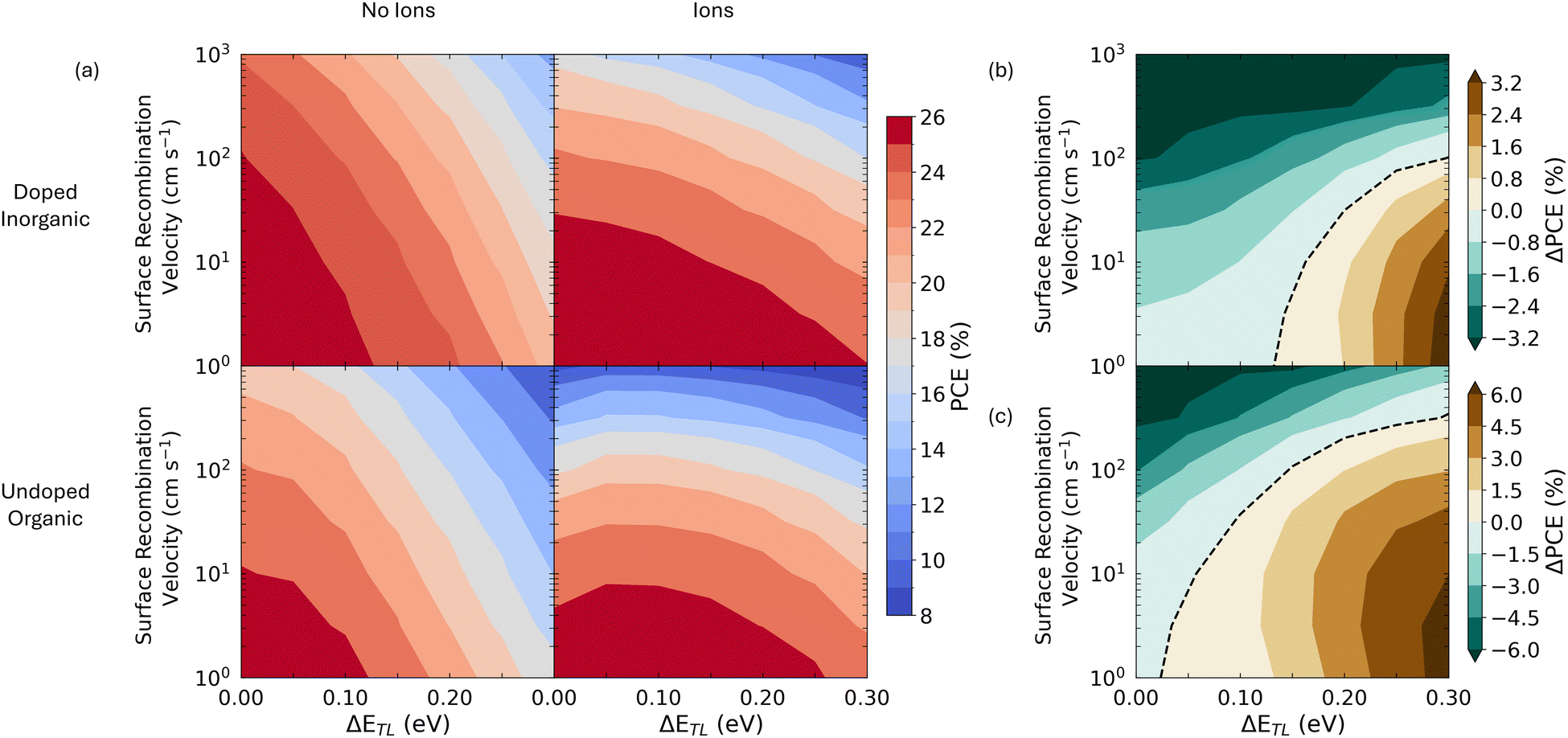 | ||
| Fig. 4 (a) A comparison of the dependence of PCE on surface recombination velocity and transport layer energetic offset (ΔETL) for simulated devices without (left-hand column) and with (right-hand column) a mobile ion density of 1018 cm−3. In the top row, we show results for devices using the doped inorganic parameter set and, in the bottom row, we show results for devices using the undoped organic parameter set. Figures (b) and (c) show the difference in PCE, defined as ΔPCE = PCE(with ions) – PCE(no ions), for (b) the doped inorganic parameter set and (c) the undoped organic parameter set. The black dashed line is a guide for the eye to indicate where ΔPCE = 0. | ||
| Change in cell design parameter | Example | Relative impact of change in cell design parameter on photovoltaic performance | |
|---|---|---|---|
| With ions | Without mobile ions | ||
| Reduce electron/hole diffusion length or increase perovskite thickness | Prolonged exposure of device to light67 | Loss in J sc | Loss in fill factor |
| Ions screen the built-in potential, which leads to charge collection being driven by diffusion (Fig. 1a)11,12,68 | Transport is drift-driven, charge collection efficiency is dependent on the applied field. (Fig. S16, ESI). | ||
| Reduce built-in potential (interface dominated recombination with low to medium rate) | Use gold as the metallic electrode in place of silver (for same device stack) | Gain in V OC | Reduction in V OC |
| Ionic charge substituted for minority electronic charge carriers at key interfaces. This results in lower recombination rates when V > Vflat (Fig. 1b and c) | Minority electronic charge carriers accumulate at key interfaces. This results in a sharp increase in recombination rates when V ≤ Vflat. (Fig. 1b and c) | ||
| Reduce built-in potential (interface dominated recombination with high rate) | Reduction in V OC | Gain in V OC | |
| Ionic charge attracts minority electronic carriers to key interfaces. This increases recombination rates when V < Vflat (Fig. S3, ESI) | The internal electric field repels minority electronic carriers from key interfaces. This results in lower recombination rates when V > Vflat (Fig. S3, ESI) | ||
| Reduce built-in potential (bulk dominated recombination, high injection limit, n ≈ p) | Reduction in J sc and V OC | Gain in J sc and V OC | |
| Ionic field screening results in greater overlap of the electron and hole populations, increasing the rate of bulk recombination processes (Fig. S3, ESI). | Presence of an electric field in the active layer reduces overlap of the electron and hole populations, decreasing the rate of bulk recombination processes (Fig. S3, ESI) | ||
| Increase energy offset between perovskite and transport layer band edges | Replace PCBM electron transport layer with C60 | Effect similar to reducing the built-in potential, refer to the relevant row above. | |
| For undoped organic transport layers, cell efficiency increases for moderate offsets due to improved extraction and smaller VOC losses (Fig. S17, ESI). | For undoped organic transport layers, negligible improvement in efficiency for moderate offsets due to efficient extraction and larger VOC losses (Fig. S17, ESI). | ||
| Dope perovskite layer | Vary perovskite precursor ratio69 | All factors described above show reduced sensitivity to mobile ions due to the greater contribution of electronic charge to the perovskite layer electrostatics28 | |
| Asymmetry in contact layer energetic offsets | Use e.g., PTAA with ICBA as the charge transport layers | Asymmetric redistribution of ionic charge and injection of electronic charge from contacts results in effective doping of the perovskite bulk by uncompensated mobile ions. All factors described above show less sensitivity to mobile ions (Supplementary Note One, ESI)28,31 | |
Conclusions
We have shown that the presence of mobile ions does not a priori reduce the maximum achievable efficiency of PSCs but does change the design regime where this maximum efficiency is attained. Using drift-diffusion simulations, we demonstrate that this is because the size of interfacial recombination currents in PSCs are less sensitive to energetic misalignments at perovskite/transport layer interfaces than in equivalent devices with no mobile ions, provided that VOC exceeds the flat band condition in the perovskite layer. This increases the range of energetic offsets for which PSCs can maintain high PCEs, although it makes them less tolerant to high values of the surface recombination velocity, which explains the field's focus on minimising interfacial recombination in recent years. Additionally, this is the first experimental demonstration that the presence of mobile ions systematically increases steady-state VOC relative to devices without mobile ions. This result was found to hold for devices using n–i–p and p–i–n architectures, with MAPI or alloyed perovskite compositions, and using a range of possible transport layer materials. Most importantly, we have shown that the effects of mobile ions are still relevant in determining the steady-state performance of highly efficient PSCs, even those which show negligible hysteresis. The close agreement of our experimental and simulated results confirms the validity of drift-diffusion simulations in describing the device physics of PSCs and provides strong evidence for our claim that mobile ions are not necessarily detrimental to the performance of PSCs. Instead, their impact on steady state PCE should be considered holistically, since it is possible for losses in photocurrent caused by ionic field screening to be compensated for by ion-mediated gains in photovoltage.Author contributions
L. J. F. H, P. C. and P. R. F. B. conceived the ideas. L. J. F. H. performed the drift-diffusion and interpreted simulations under the supervision of J. R. D. and P. R. F. B. Stabilise and Pulse measurements were performed by F. J. A. under the supervision of P. D. Triple cation perovskite solar cells were fabricated by Y. L and A. K under the supervision of A. B. D. L. J. F. H wrote the manuscript. All authors discussed the results and reviewed the manuscript.Data availability
Data used to generate the main text figures in this article are available at https://doi.org/10.5281/zenodo.12761597. The Driftfusion code used in this paper can be found at https://github.com/lucy-hart/Driftfusion/tree/MobileIonsImproveTheDesignTolerancesOfPSCs. The parameters used in generating the simulation results have been included as part of the ESI† and can also be found in the Input_files folder of the above link.Conflicts of interest
There are no conflicts to declare.Acknowledgements
For this work, L. J. F. H., P. R. F. B. and J. R. D. thank the EPSRC ATIP project (EP/TO28513/1). F. J. A. and P. D. thank the EPSRC and the University of Glasgow. A. B. D., Y. L. and A. K. acknowledge support from Seed Funding for Basic Research of the University of Hong Kong.References
- H. Min, D. Y. Lee, J. Kim, G. Kim, K. S. Lee, J. Kim, M. J. Paik, Y. K. Kim, K. S. Kim, M. G. Kim, T. J. Shin and S. I. Seok, Nature, 2021, 598, 444–450 CrossRef CAS PubMed.
- J. Park, J. Kim, H.-S. Yun, M. J. Paik, E. Noh, H. J. Mun, M. G. Kim, T. J. Shin and S. I. Seok, Nature, 2023, 616, 724–730 CrossRef CAS PubMed.
- A. Senocrate, I. Moudrakovski, G. Y. Kim, T.-Y. Yang, G. Gregori, M. Grätzel and J. Maier, Angew. Chem., Int. Ed., 2017, 56, 7755–7759 CrossRef CAS PubMed.
- T.-Y. Yang, G. Gregori, N. Pellet, M. Grätzel and J. Maier, Angew. Chem., Int. Ed., 2015, 54, 7905–7910 CrossRef CAS PubMed.
- C. Eames, J. M. Frost, P. R. F. Barnes, B. C. O’Regan, A. Walsh and M. Saiful Islam, Nat. Commun., 2015, 6, 7497 CrossRef CAS PubMed.
- J. Haruyama, K. Sodeyama, L. Han and Y. Tateyama, J. Am. Chem. Soc., 2015, 137, 10048–10051 CrossRef CAS PubMed.
- N. E. Courtier, J. M. Cave, J. M. Foster, A. B. Walker and G. Richardson, Energy Environ. Sci., 2019, 12, 396–409 RSC.
- N. E. Courtier, Phys. Rev. Appl., 2020, 14, 024031 CrossRef CAS.
- D. Moia and J. Maier, ACS Energy Lett., 2021, 6, 1566–1576 CrossRef CAS.
- J. Thiesbrummel, V. M. Le Corre, F. Peña-Camargo, L. Perdigón-Toro, F. Lang, F. Yang, M. Grischek, E. Gutierrez-Partida, J. Warby, M. D. Farrar, S. Mahesh, P. Caprioglio, S. Albrecht, D. Neher, H. J. Snaith and M. Stolterfoht, Adv. Energy Mater., 2021, 11, 2101447 CrossRef CAS.
- V. M. Le Corre, J. Diekmann, F. Peña-Camargo, J. Thiesbrummel, N. Tokmoldin, E. Gutierrez-Partida, K. P. Peters, L. Perdigón-Toro, M. H. Futscher, F. Lang, J. Warby, H. J. Snaith, D. Neher and M. Stolterfoht, Solar RRL, 2022, 6, 2100772 CrossRef CAS.
- W. Xu, L. J. F. Hart, B. Moss, P. Caprioglio, T. J. Macdonald, F. Furlan, J. Panidi, R. D. J. Oliver, R. A. Pacalaj, M. Heeney, N. Gasparini, H. J. Snaith, P. R. F. Barnes and J. R. Durrant, Adv. Energy Mater., 2023, 13, 2301102 CrossRef CAS.
- S. Kim, S. Bae, S.-W. Lee, K. Cho, K. D. Lee, H. Kim, S. Park, G. Kwon, S.-W. Ahn, H.-M. Lee, Y. Kang, H.-S. Lee and D. Kim, Sci. Rep., 2017, 7, 1200 CrossRef PubMed.
- J. Li, Q. Dong, N. Li and L. Wang, Adv. Energy Mater., 2017, 7, 1602922 CrossRef.
- J.-W. Lee, S.-G. Kim, J.-M. Yang, Y. Yang and N.-G. Park, APL Mater., 2019, 7, 041111 CrossRef.
- S. Akel, A. Kulkarni, U. Rau and T. Kirchartz, PRX Energy, 2023, 2, 013004 CrossRef.
- E. Bi, H. Chen, F. Xie, Y. Wu, W. Chen, Y. Su, A. Islam, M. Grätzel, X. Yang and L. Han, Nat. Commun., 2017, 8, 15330 CrossRef CAS PubMed.
- R. Wang, J. Xie, L. Meng, J.-W. Lee, Z. Zhao, P. Sun, L. Cai, T. Huang, Z. Wang, Z.-K. Wang, Y. Duan, J. L. Yang, S. Tan, Y. Yuan, Y. Huang and Y. Yang, Joule, 2019, 3, 1464–1477 CrossRef CAS.
- H. Zhu, S. Teale, M. N. Lintangpradipto, S. Mahesh, B. Chen, M. D. McGehee, E. H. Sargent and O. M. Bakr, Nat. Rev. Mater., 2023, 8, 569–586 CrossRef.
- S. Wu, R. Chen, S. Zhang, B. H. Babu, Y. Yue, H. Zhu, Z. Yang, C. Chen, W. Chen, Y. Huang, S. Fang, T. Liu, L. Han and W. Chen, Nat. Commun., 2019, 10, 1161 CrossRef PubMed.
- A. Walsh, D. O. Scanlon, S. Chen, X. G. Gong and S.-H. Wei, Angew. Chem., Int. Ed., 2015, 54, 1791–1794 CrossRef CAS PubMed.
- J. Kim, S.-H. Lee, J. H. Lee and K.-H. Hong, J. Phys. Chem. Lett., 2014, 5, 1312–1317 CrossRef CAS PubMed.
- W.-J. Yin, T. Shi and Y. Yan, Appl. Phys. Lett., 2014, 104, 063903 CrossRef.
- D. Meggiolaro, S. G. Motti, E. Mosconi, A. J. Baker, J. Ball, C. A. R. Perini, F. Deschler, A. Petrozza and F. De Angelis, Energy Environ. Sci., 2018, 11, 702–713 RSC.
- M.-H. Du, J. Phys. Chem. Lett., 2015, 6, 1461–1466 CrossRef CAS PubMed.
- C. Ahläng, M. Nyman and R. Österbacka, Phys. Rev. Appl., 2021, 16, 014041 CrossRef.
- N. Mozaffari, D. Walter, T. P. White, A. D. Bui, G. Dansoa Tabi, K. Weber and K. R. Catchpole, Solar RRL, 2022, 6, 2101087 CrossRef CAS.
- N. Wu, D. Walter, A. Fell, Y. Wu and K. Weber, J. Phys. Chem. C, 2020, 124, 219–229 CrossRef CAS.
- D. A. Jacobs, Y. Wu, H. Shen, C. Barugkin, F. J. Beck, T. P. White, K. Weber and K. R. Catchpole, Phys. Chem. Chem. Phys., 2017, 19, 3094–3103 RSC.
- W. Tress, J. Phys. Chem. Lett., 2017, 8, 3106–3114 CrossRef CAS PubMed.
- M. Córdoba and K. Taretto, Solar RRL, 2023, 8, 2300742 CrossRef.
- S. Lin, B. Yang, X. Qiu, J. Yan, J. Shi, Y. Yuan, W. Tan, X. Liu, H. Huang, Y. Gao and C. Zhou, Org. Electron., 2018, 53, 235–241 CrossRef CAS.
- X. Gong, Q. Sun, S. Liu, P. Liao, Y. Shen, C. Grätzel, S. M. Zakeeruddin, M. Grätzel and M. Wang, Nano Lett., 2018, 18, 3969–3977 CrossRef CAS PubMed.
- X. Huang, J. Du, X. Guo, Z. Lin, J. Ma, J. Su, L. Feng, C. Zhang, J. Zhang, J. Chang and Y. Hao, Solar RRL, 2020, 4, 1900336 CrossRef CAS.
- C. A. Aranda, A. O. Alvarez, V. S. Chivrony, C. Das, M. Rai and M. Saliba, Joule, 2024, 8, 241–254 CrossRef CAS.
- P. Calado, I. Gelmetti, B. Hilton, M. Azzouzi, J. Nelson and P. R. F. Barnes, J. Comput. Electron., 2022, 21, 960–991 CrossRef CAS.
- Y. Wang, J. Lin, Y. He, Y. Zhang, Q. Liang, F. Liu, Z. Zhou, C. C. S. Chan, G. Li, S.-P. Feng, A. M. C. Ng, K. S. Wong, J. Popović and A. B. Djurišić, Solar RRL, 2022, 6, 2200224 CrossRef CAS.
- R. S. Bonilla, B. Hoex, P. Hamer and P. R. Wilshaw, Phys. Status Solidi A, 2017, 214, 1700293 CrossRef.
- S. Bitton and N. Tessler, Energy Environ. Sci., 2023, 16, 2621–2628 RSC.
- D. A. Eggesr, L. Kronik and A. M. Rappe, Angew. Chem., Int. Ed., 2015, 54, 12437–12441 CrossRef PubMed.
- H. J. van Daal, J. Appl. Phys., 2003, 39, 4467–4469 CrossRef.
- Y. Chen, Q. Meng, L. Zhang, C. Han, H. Gao, Y. Zhang and H. Yan, J. Energy Chem., 2019, 35, 144–167 CrossRef.
- T. Yokoyama, Y. Nishitani, Y. Miyamoto, S. Kusumoto, R. Uchida, T. Matsui, K. Kawano, T. Sekiguchi and Y. Kaneko, ACS Appl. Mater. Interfaces, 2020, 12, 27131–27139 CrossRef CAS PubMed.
- F. M. Rombach, S. A. Haque and T. J. Macdonald, Energy Environ. Sci., 2021, 14, 5161–5190 RSC.
- L. Nakka, Y. Cheng, A. G. Aberle and F. Lin, Adv. Energy Sustainability Res., 2022, 3, 2200045 CrossRef CAS.
- F. Ye, S. Zhang, J. Warby, J. Wu, E. Gutierrez-Partida, F. Lang, S. Shah, E. Saglamkaya, B. Sun, F. Zu, S. Shoaee, H. Wang, B. Stiller, D. Neher, W.-H. Zhu, M. Stolterfoht and Y. Wu, Nat. Commun., 2022, 13, 7454 CrossRef CAS PubMed.
- D. Yang, X. Zhang, K. Wang, C. Wu, R. Yang, Y. Hou, Y. Jiang, S. Liu and S. Priya, Nano Lett., 2019, 19, 3313–3320 CrossRef CAS PubMed.
- M. Stolterfoht, P. Caprioglio, C. M. Wolff, J. A. Márquez, J. Nordmann, S. Zhang, D. Rothhardt, U. Hörmann, Y. Amir, A. Redinger, L. Kegelmann, F. Zu, S. Albrecht, N. Koch, T. Kirchartz, M. Saliba, T. Unold and D. Neher, Energy Environ. Sci., 2018, 12, 2778–2788 RSC.
- C. M. Wolff, P. Caprioglio, M. Stolterfoht and D. Neher, Adv. Mater., 2019, 31, 1902762 CrossRef CAS PubMed.
- J. Warby, F. Zu, S. Zeiske, E. Gutierrez-Partida, L. Frohloff, S. Kahmann, K. Frohna, E. Mosconi, E. Radicchi, F. Lang, S. Shah, F. Peña-Camargo, H. Hempel, T. Unold, N. Koch, A. Armin, F. De Angelis, S. D. Stranks, D. Neher and M. Stolterfoht, Adv. Energy Mater., 2022, 12, 2103567 CrossRef CAS.
- T. S. Sherkar, C. Momblona, L. Gil-Escrig, J. Avila, M. Sessolo, H. J. Bolink and L. Jan Anton Koster, ACS Energy Lett., 2017, 2, 1214–1222 CrossRef CAS PubMed.
- N. S. Hill, M. V. Cowley, N. Gluck, M. H. Fsadni, W. Clarke, Y. Hu, M. J. Wolf, N. Healy, M. Freitag, T. J. Penfold, G. Richardson, A. B. Walker, P. J. Cameron and P. Docampo, Adv. Mater., 2023, 35, 2302146 CrossRef CAS PubMed.
- H. Wang, M. Zhou and H. Luo, ACS Omega, 2018, 3, 1445–1450 CrossRef CAS PubMed.
- S. van Reenen, M. Kemerink and H. J. Snaith, J. Phys. Chem. Lett., 2015, 6, 3808–3814 CrossRef CAS PubMed.
- J. A. Christians, J. S. Manser and P. V. Kamat, J. Phys. Chem. Lett., 2015, 6, 852–857 CrossRef CAS PubMed.
- R. B. Dunbar, B. C. Duck, T. Moriarty, K. F. Anderson, N. W. Duffy, C. J. Fell, J. Kim, A. Ho-Baillie, D. Vak, T. Duong, Y. Wu, K. Weber, A. Pascoe, Y.-B. Cheng, Q. Lin, P. L. Burn, R. Bhattacharjee, H. Wang and G. J. Wilson, J. Mater. Chem. A, 2017, 5, 22542–22558 RSC.
- J. Thiesbrummel, S. Shah, E. Gutierrez-Partida, F. Zu, F. Peña-Camargo, S. Zeiske, J. Diekmann, F. Ye, K. P. Peters, K. O. Brinkmann, P. Caprioglio, A. Dasgupta, S. Seo, F. A. Adeleye, J. Warby, Q. Jeangros, F. Lang, S. Zhang, S. Albrecht, T. Riedl, A. Armin, D. Neher, N. Koch, Y. Wu, V. M. Le Corre, H. Snaith and M. Stolterfoht, Nat. Energy, 2024, 9, 664–676 CrossRef CAS.
- L. Bertoluzzi, C. C. Boyd, N. Rolston, J. Xu, R. Prasanna, B. C. O’Regan and M. D. McGehee, Joule, 2020, 4, 109–127 CrossRef CAS.
- M. Sajedi Alvar, P. W. M. Blom and G.-J. A. H. Wetzelaer, Adv. Electron. Mater., 2020, 6, 1900935 CrossRef CAS.
- S. G. McCallum, O. Nicholls, K. O. Jenson, M. V. Cowley, J. E. Lerpinière and A. B. Walker, J. Phys. Energy, 2023, 6, 015005 CrossRef.
- K. Wojciechowski, S. D. Stranks, A. Abate, G. Sadoughi, A. Sadhanala, N. Kopidakis, G. Rumbles, C.-Z. Li, R. H. Friend, A. K.-Y. Jen and H. J. Snaith, ACS Nano, 2014, 8, 12701–12709 CrossRef CAS PubMed.
- Z.-W. Gao, Y. Wang and W. C. H. Choy, Adv. Energy Mater., 2022, 12, 2104030 CrossRef CAS.
- X. Liu, K.-W. Tsai, Z. Zhu, Y. Sun, C.-C. Chueh and A. K.-Y. Jen, Adv. Mater. Interfaces, 2016, 3, 1600122 CrossRef.
- S. Ravishankar, Z. Liu, U. Rau and T. Kirchartz, PRX Energy, 2022, 1, 013003 CrossRef.
- O. Almora, C. Aranda, E. Mas-Marzá and G. Garcia-Belmonte, Appl. Phys. Lett., 2016, 109, 173903 CrossRef.
- F. Peña-Camargo, J. Thiesbrummel, H. Hempel, A. Musiienko, V. M. Le Corre, J. Diekmann, J. Warby, T. Unold, F. Lang, D. Neher and M. Stolterfoht, Appl. Phys. Rev., 2022, 9, 021409 Search PubMed.
- J. Wei, Q. Wang, J. Huo, F. Gao, Z. Gan, Q. Zhao and H. Li, Adv. Energy Mater., 2021, 11, 2002326 CrossRef CAS.
- S. Akel, A. Kulkarni, U. Rau and T. Kirchartz, PRX Energy, 2023, 2, 013004 CrossRef.
- J. Euvrard, Y. Yan and D. B. Mitzi, Rev. Mater., 2021, 6, 531–549 CrossRef CAS.
Footnote |
| † Electronic supplementary information (ESI) available: Supplementary information Includes extended methods, Tables, Images and Notes. See DOI: https://doi.org/10.1039/d4ee02669a |
| This journal is © The Royal Society of Chemistry 2024 |