Formation and structural observation of cesium encapsulated single-walled carbon nanotubes†
Goo-Hwan
Jeong
*a,
Rikizo
Hatakeyama
a,
Takamichi
Hirata
a,
Kazuyuki
Tohji
a,
Kenichi
Motomiya
a,
Toshie
Yaguchi
b and
Yoshiyuki
Kawazoe
c
aGraduate School of Engineering, Tohoku University, Sendai 980-8579, Japan
bApplication Technology Dept, Techno Research Lab, Hitachi Science System, Hitachinaka-shi 312-8504, Japan
cInstitute for Materials Research, Tohoku University, Sendai 980-8577, Japan. E-mail: hatak17@ec.ecei.tohoku.ac.jp; Fax: +81-22-263-9225
First published on 5th December 2002
Abstract
Cesium encapsulation inside single-walled carbon nanotubes (SWNTs) is for the first time realized by ion irradiation of SWNTs immersed in a magnetized alkali-metal plasma, the configuration of which is confirmed to comprise three varieties by field emission type transmission electron microscopy (FE-TEM) and scanning TEM (STEM) observation.
It is a very fascinating fact that SWNTs1 can intercalate foreign atoms and molecules such as fullerenes, endohedral-metallofullerenes, alkali metals or other compounds.2–6 These materials are expected to have novel properties and are predicted to be utilizable in various fields such as superconductor, nano-scale electronic devices, bio-materials and so on. Up to now, vapor deposition by thermally diffused elements and capillary wetting method have been extensively used for elements encapsulation.7,8 Although high yields of intercalated nanotubes are reported, there remain some problems, for example, difficulty in controlling intercalant fluxes and the disadvantage of a time-consuming process. Furthermore, that only one species can be intercalated at one process would be a critical barrier to more extensive application. For this reason, we attempted a new experimental approach using plasma irradiation methods, where various kinds of atoms, molecules or their combinations can be selectively encapsulated inside the SWNTs. Recently, we have reported the formation of C60 encapsulated SWNTs9 using an alkali-fullerene plasma system, which is proved to be due to the structural modification of SWNTs. As a development of this work, our concern is here focused on the experimental elucidation of intercalating the alkali-metal Cs inside the SWNTs..
The synthesis of single-walled carbon nanotubes was basically carried out by an electric-arc discharge. Typical bundle-type tubes were produced by using Fe–Ni catalyst; sea-urchin type tubes, on the other hand, were synthesized by Se catalyst mixed in an anode graphite rod. The raw soot was purified by oxidation, filtration and hydrochloric acid washing, HIDE method.10 Purified SWNTs paper was dispersed by brief sonication in ethanol, then droplets of this suspension were dripped and dried on stainless steel substrates (15 mm × 15 mm). The details of the production of a Cs-fullerene plasma consisting of Cs+, C60−, and residual electrons are similar to those for other alkali-fullerene plasmas, described elsewhere.11 When DC bias voltages (φap) are applied to the substrate in the plasma with respect to a grounded plasma-source electrode, positive Cs and negative C60 ions are substantially accelerated by plasma sheaths in front of the substrate, impinging on the SWNTs bundles for φap < 0 and φap > 0, respectively. Such a plasma irradiation is carried out for 1 h. FE-TEM (Hitachi HF-2000), which is operated at 200 kV, having a point-to-point resolution of 0.23 nm and equipped with energy dispersive X-ray spectrometry (EDS, Noran Instruments) is used for the detailed observation and chemical element detection. The Z-contrast technique by STEM (Hitachi HD-2000),12 which is capable of chemical element mapping on the nanometer-scale, is adopted for the Cs confirmation in the Cs intercalated SWNTs.
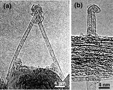
Fig. 1 shows FE-TEM images of the sample treated with φap = 20 V in the Cs-fullerene plasma. The generation of dislocated individual tube is clearly demonstrated in Fig. 1(a), which is also observed under the conditions of 5 < φap < 20 V and φap < −100 V in the cases of C60− and Cs+ irradiation, respectively. Considering the absolute value of applied bias voltage and bombarding ion mass (C60− = 720 and Cs+ = 133) in provoking structural deformation, it is concluded that these structurally-modified nanotubes are mainly produced by momentum transfer from the accelerated charged particles to the nanotubes. Fig. 1(b) shows a typical image which evidently demonstrates the synthesis of C60 encapsulated SWNTs. The production rate of this material is about 50∼60% in the case of plasma density 1010 cm−3. The encapsulation yield is estimated on the basis of the length of encapsulated parts to the total length of clearly visible nanotubes in the highly resolved image taken by FE-TEM. The encapsulation yield is found to obviously increase with increasing plasma density because higher plasma density means increased irradiation ion-flux, which may be crucial in the enhancement of the encapsulation rate. The quantitative estimation of this relationship between the plasma density and encapsulation efficiency will be reported elsewhere.
 | ||
| Fig. 1 (a) FE-TEM image showing a dislocated, open-ended individual nanotube, presumably caused by C60 negative-ion impact (φap = 20 V) in the Cs-C60 plasma. (b) SWNTs encapsulating a set of fullerene molecules are clearly shown. | ||
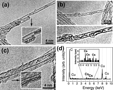
Fig. 2 gives FE-TEM images and the EDS spectrum obtained from samples treated with φap = −100 V in the Cs plasma. The linear and spiral configurations of intercalated Cs are clearly shown in Fig. 2(a) and 2(b), respectively. The inset in (a) stresses the intercalated Cs by dotting with black circles and bottom image in (b) is also marked by dotting for a spiral chain of intercalated Cs inside the individual nanotube bridging two nanotube bundles. A helix configuration of intercalants inside the SWNTs is recently predicted in the case of iodine intercalation by the capillary wetting method.13 In Fig. 2(c), on the other hand, we can find 2 or 3 individual nanotubes combined with each other by Van der Waals attraction. Although the upper tube looks vacant, the lower tube is observed to be partially intercalated and, presumably, crystallized. The inset especially reveals the regularly located 2 rows of Cs. As to Cs+ intercalation inside the (10, 10) nanotube, Cs crystallization is basically possible according to a comparison of their diameters . The diameter of the (10, 10) tube is generally known to be about 13.6 Å and the π electron-cloud thickness is considered to be 1.7 Å. Therefore, the inner space of the (10, 10) tube is approximately 10.2 Å in diameter. Judging from this structural comparison, there remains a 3.52 Å space between 2 rows of 3.34 Å diameter Cs+. Strictly speaking, the accurate encapsulation site of Cs+ has to be determined on the basis of a comprehensive understanding of the details of the interaction energy between the tube wall and intercalant, which is governed by the competition between Van der Waals and coulombic forces. Here, in order to obtain more accurate compositional information from a very thin and isolated SWNT bundle, in situ EDS analysis was performed during the FE-TEM observation. However, in the case of elemental mapping or line scanning, the amount of Cs inside the tubes seemed to be lower than the detection limit of the EDS analysis. Therefore, we used a compressed electron beam (∼5 nm diameter) in the analysis, which inevitably yielded a relatively weak intensity for the Cs spectrum-peak. In any case, the result well indicated the existence of Cs in the irradiated SWNTs, as shown in Fig. 2(d).
 | ||
| Fig. 2 TEM images and the EDS spectrum obtained from samples treated with φap = −100 V in the Cs plasma. (a) Linear configuration of intercalated Cs. The inset underlines the intercalated Cs by dotting with black circles. (b) Spiral chain of intercalated Cs inside the individual nanotube bridging two bundles. Upper image is the original and bottom is an image marked with dots tracing the Cs. (c) Although the upper tube is hollow, the lower tube is partially intercalated and crystallized. The inset emphasizes the crystallization of Cs. (d) EDS result recorded from very thin bundles composed of 4–5 individual tubes reveals the existence of Cs. | ||
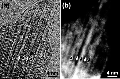
In order to get highly reliable information about the Cs intercalated SWNTs, the Z-contrast technique was adopted and a typical result is shown in Fig. 3. Large contrast differences in the Z-contrast image originate from the intensity differences of high-angle scattered electrons, which are proportional to the differences in the squares of the atomic numbers (Cs = 55 and C = 6).14 Therefore, Cs intercalated tubes (black arrows) shown darker than neighboring hollow tubes (white arrows) in Fig. 3(a) are distinguished by bright stripes of 2 nm diameter in Fig. 3(b). It is reasonable that the positions of Cs intercalated tubes in Fig. 3(a) exactly coincide with the bright lines in the dark field image in Fig. 3(b).
 | ||
| Fig. 3 (a) Bright-field image of sea-urchin type SWNTs irradiated by φap = −100 V in the Cs plasma. (b) Corresponding Z-contrast image clearly shows the partial intercalation of Cs by contrast difference. Cs intercalated tubes indicated by black arrows are seen darker than surrounding tubes in (a) and coincide well with the brighter tubes in (b), which means Cs intercalation. | ||
Although a thorough and overall understanding is necessary to elucidate the various Cs configurations inside the individual nanotubes, the formation of Cs encapsulated SWNTs, not surface adsorption, is for the first time verified in our experiment. This has not been previously reported to the best of our knowledge. Finally, the present result gives us confidence that our new approach has high feasibility for the realization of carbon nanotubes with novel functionality.
The authors would like to thank Dr A. A. Farajian for his valuable discussion. G.-H. Jeong thanks the Sasakawa Scientific Research Grant from The Japan Science Society for partial financial support. Part of this work was carried out under the Cooperative Research Project Program of the Research Institute of Electrical Communication, Tohoku University. This work was also supported by a Grant-in-Aid for Scientific Research from the Ministry of Education, Culture, Sports, Science, and Technology, Japan.
Notes and references
- S. Iijima and T. Ichihashi, Nature, 1993, 363, 603 CrossRef CAS.
- B. W. Smith, M. Monthioux and D. E. Luzzi, Nature, 1998, 396, 323 CrossRef CAS.
- K. Suenaga, M. Tence, C. Mory, C. Colliex, H. Kato, T. Okazaki, H. Shinohara, K. Hirahara, S. Bandow and S. Iijima, Science, 2000, 290, 2280 CrossRef CAS.
- R. S. Lee, H. J. Kim, J. E. Fischer, A. Thess and R. E. Smalley, Nature, 1997, 388, 255 CrossRef CAS.
- R. R. Meyer, J. Sloan, R. E. Dunin-Borkowski, A. I. Kirkland, M. C. Novotny, S. R. Bailey, J. L. Hutchison and M. L. H. Green, Science, 2000, 289, 1324 CrossRef CAS.
- J. Sloan, A. I. Kirkland, J. L. Hutchison and M. L. H. Green, Chem. Commun., 2002, 1319 RSC.
- K. Hirahara, K. Suenaga, S. Bandow, H. Kato, T. Okazaki, H. Shinohara and S. Iijima, Phys. Rev. Lett., 2000, 85(25), 5384 CrossRef CAS.
- P. M. Ajayan and S. Iijima, Nature, 1993, 361, 333 CrossRef CAS.
- G.-H. Jeong, R. Hatakeyama, T. Hirata, K. Tohji, K. Motomiya, N. Sato and Y. Kawazoe, Appl. Phys. Lett., 2001, 79, 4213 CrossRef CAS.
- K. Tohji, T. Goto, H. Takahashi, Y. Shinoda, N. Shimizu, B. Jeyadevan, I. Matsuoka, Y. Saito, A. Kasuya, T. Ohsuna, K. Hiraga and Y. Nishina, Nature, 1996, 383(24), 679 CrossRef CAS.
- N. Sato, T. Mieno, T. Hirata, Y. Yagi, R. Hatakeyama and S. Iizuka, Phys. Plasmas, 1994, 1, 3480 CrossRef CAS.
- http://www.hitachi-hitec.com/science/english/product/tem/hd2000.html.
- X. Fan, E. C. Dickey, P. C. Eklund, K. A. Williams, L. Grigorian, R. Buczko, S. T. Pantelides and S. J. Pennycook, Phys. Rev. Lett., 2000, 84(20), 4621 CrossRef CAS.
- P. D. Nellist and S. J. Pennycook, Science, 1996, 274, 413 CrossRef CAS.
Footnote |
| † Electronic supplementary information (ESI) available: bright-field STEM images and their corresponding Z-contrast images composed of Cs inside filled and outside doped SWNTs are given. See http://www.rsc.org/suppdata/cc/b2/b210079g/ |
| This journal is © The Royal Society of Chemistry 2003 |
