Synthesis of carbon nitride nanotubes with the C3N4 stoichiometry via a benzene-thermal process at low temperatures†
Qixun
Guo
,
Yi
Xie
*,
Xinjun
Wang
,
Shuyuan
Zhang
,
Tao
Hou
and
Shichang
Lv
Structure Research Laboratory and Department of Chemistry, University of Science and Technology of China, Hefe, Anhui 230026, P. R. China. E-mail: yxielab@ustc.edu.cn; Fax: 86-551-3603987; Tel: 86-551-3603987
First published on 21st November 2003
Abstract
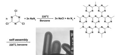
In this communication, we first report the direct synthesis of high-quality carbon nitride nanotubes (CNNTs) with inner diameters of 50–100 nm and wall thicknesses of 20–50 nm with the C3N4 stoichiometry on a high-yield of 40% via a simple benzene-thermal process involving the reaction of C3N3Cl3 with NaN3 in a Teflon-lined autoclave at 220 °C without using any catalyst or template.
The discovery of carbon nanotubes1 as new form of matter in the nanoscale range has opened a new challenging field in solid state physics, chemistry, and materials science due to their potential applications. Since then, much attention has been paid to the preparation of nanotubes of various solids.2–3
In 1989, Liu and Cohen theoretically predicted that the covalent carbon-nitrogen solid, β-C3N4, which has a similar structure to β-Si3N4, would have a bulk modulus comparable to or greater than that of the hardest known materials, diamond.4 During the past few years, five different structures have been predicted: one is two-dimensional (graphitic-C3N4) and four are three-dimensional (α-C3N4, β-C3N4, cubic-C3N4, and pseudocubic-C3N4). Recently, much attentions in theory are focused on the graphitic forms of carbon nitride, g-C3N4, for their potential applications as precursor for carbon nitride nanotubes and superhard forms.5–8 So far there are no reports to claim the synthesis of carbon nitride nanotubes with the C3N4 stoichiometry in experiment. The synthesis of carbon nitride with a high nitrogen content is difficult due to the greater thermodynamic stability of carbon and separate nitrogen molecules.9 This is likely the reason for the failure of various physical and chemical deposition methods to produce materials with bulk C3N4 composition.10 Recently, Gillan's group has successfully synthesized nitrogen-rich carbon nitride networks and carbon nitride films from an energetic molecular azide precursor.11,12 Here we report the synthesis of high nitrogen-content carbon nitride nanotubes (CNNTs) with the C3N4 stoichiometry via a benzene-thermal process under mild conditions for the first time. The high quality carbon nitride nanotubes with the yield of 40% were obtained by this route. This result will give us a guideline for the design and synthesis of carbon nitride nanotube structures.
In a typical procedure, 1.84 g C3N3Cl3 (1,3,5-trichlorotriazine) and 1.96 g NaN3 (sodium azide) powders were put into a 50 mL Teflon-lined autoclave which was filled with 35 mL benzene. All of the above manipulations were performed in a glove-box with flowing nitrogen gas. The autoclave was sealed and maintained at 220 °C for 15 h and then allowed to cool to room temperature naturally. The brown precipitate was collected and washed three times with benzene, then washed three times with distilled water. After that, the obtained sample was dried in vacuum at 50 °C for 6 h.
From the Electron Microscopy images (TEM‡ shown in Figs. 1a and 1d, SEM§ shown in Fig. 1b, and HRTEM¶ shown in Fig. 1c), one can see that the inner diameters of nanotubes is 50–100 nm and wall thicknesses is 20–50 nm and lengths ranges from hundreds of nanometers to about two micrometers with most nanotubes having closed ends and a few having one open ends.
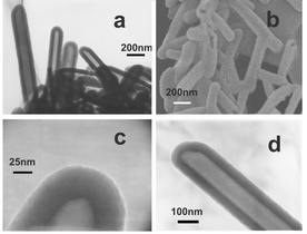 | ||
| Fig. 1 (a) a typical TEM image of the synthesized CNNTs; (b) field-emission SEM image of the CNNTs; (c) HRTEM image of a tubular structure of a CNNT; (d) TEM image of a typical CNNT. | ||
In the electron microdiffaction these nanotubes exhibit very weak diffuse ring patterns, indicating a highly disordered wall microstructures, which agrees with the HRTEM observation (Fig. 1c) of disordered multilayered wall. The XRD|| (see ESI†) shows a single broad peak centered at 25 degrees corresponding to interlayer d spacing of 0.35 nm, very close to the interlayer spacing (0.34 nm) of carbon nanotubes13 built from rolled graphene sheets. The observed larger d spacing (0.35 nm) in carbon nitride nanotubes than that predicted for g-C3N4 (0.33 nm)10 seems reasonable in view of the increased interlayer spacing (0.34 nm) in the multi-wall carbon nanotubes with respect to interplanar distance (0.33 nm) in graphite. The difference of the interlayer spacing between carbon nitride nanotubes and g-C3N4, 0.02 nm, is larger than that between carbon nanotubes and graphite, 0.01 nm, which may be attributed to the poor crystallization of carbon nitride nanotubes in comparison with carbon nanotubes.
XPS** measurements indicated that the C1s and N1s binding energies in the synthesized sample are 288.0, 398.75, and 400.25 eV, respectively (Fig. 2), which can be attributed to the sp2 C, sp2 N2, and sp2 N1
(labeled in Fig. 3). The observed C1s and N1s binding energies are comparable to those found in melanmine (C3N6H6) molecules with covalent C–N bonds which is very similar to the C–N bonds of carbon nitride.14 The XPS data give an evidence for the existence of graphite-like sp2 bonded structure in carbon nitride (Fig. 3). The peaks at the position of 401.60, 404.95eV may be attributed to the –NH2 or ![[double bond, length as m-dash]](https://www.rsc.org/images/entities/char_e001.gif) NH groups and π-excitations, respectively. The determined, by XPS analysis, atomic N : C ratio (1.40) in the prepared materials is good agreement with the C3N4 stoichiometry, which is similar to the C : N atomic ratio of about 1 : 1.25 obtained by Elemental analysis. In addition, about 0.5 wt% hydrogen element in the sample was detected by elemental analysis.††
NH groups and π-excitations, respectively. The determined, by XPS analysis, atomic N : C ratio (1.40) in the prepared materials is good agreement with the C3N4 stoichiometry, which is similar to the C : N atomic ratio of about 1 : 1.25 obtained by Elemental analysis. In addition, about 0.5 wt% hydrogen element in the sample was detected by elemental analysis.††
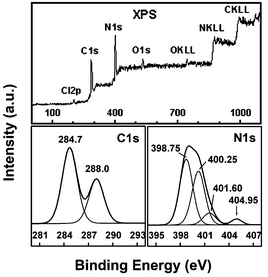 | ||
| Fig. 2 The XPS spectrum of the obtained sample. | ||
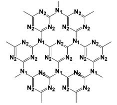 | ||
| Fig. 3 Atomic structure of a graphitic carbon nitride (g-C3N4) single layer. Nitrogen atoms occupy two different types of positions in the layer, labeled 1 and 2 in the figure. | ||
The FTIR‡‡ spectrum (Figure 4a) implies the existence of graphite-like sp2 bonded structure. The spectrum of the brown product shows broad band of the stretching modes of NH2 or NH groups at 3338 and 3210 cm−1. The absorption band centered at 1552 cm−1 is attributed to C![[double bond, length as m-dash]](https://www.rsc.org/images/entities/char_e001.gif) N, the one at 1328 cm−1 to C–N, and the one at 2138 cm−1 to C
N, the one at 1328 cm−1 to C–N, and the one at 2138 cm−1 to C![[triple bond, length as m-dash]](https://www.rsc.org/images/entities/char_e002.gif) N. The peak at 800 cm−1 belongs to s-triazine ring modes.15 Elemental analysis and FTIR showed that there are a small amount of hydrogen element and/or N–H bonds in the sample. This may be attributed to the hydrogenation of a small amount of nitrogen atoms.16
N. The peak at 800 cm−1 belongs to s-triazine ring modes.15 Elemental analysis and FTIR showed that there are a small amount of hydrogen element and/or N–H bonds in the sample. This may be attributed to the hydrogenation of a small amount of nitrogen atoms.16
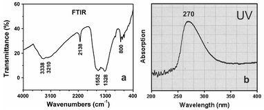 | ||
| Fig. 4 (a) a typical FTIR spectrum of the prepared sample. (b) UV spectrum of ethanol solution of the product. | ||
The presence of s-triazine ring in single layer of carbon nitride nanotubes is also evidenced by UV-vis§§ studies. The observed strong absorption band centered at 270 nm (Fig. 4b) lies in the range characteristic for π→π* electronic transition in the aromatic 1,3,5-triazine compounds.15
In summary, we have successfully synthesized high-quality carbon nitride nanotubes with the C3N4 stoichiometry on a high-yield of 40% via a simple benzene-thermal process at low temperatures without using any catalyst or template for the first time. More importantly, this high quality carbon nitride nanotubes, synthesized reproducibly in gram quantities under mild conditions, may provide researchers an opportunity to investigate the electrical and optical characteristics of these carbon nitride nanotubes in detail, which are expected as the future nanoscale devices.
Financial support from the Chinese National Science Foundation of Natural Science Research and the Chinese Ministry of Education is gratefully Acknowledged.
Notes and references
- S. Iijima, Nature, 1991, 354, 56 CrossRef CAS.
- N. G. Chopra, R. J. Luyken, K. Cherrey, V. H. Crespi, M. L. Cohen, S. G. Louie and A. Zettl, Science, 1995, 269, 966 CAS.
- J. Goldberger, R. R. He, Y. F. Zhang, S. W. Lee, H. Q. Yan, H. J. Choi and P. D. Yang, Nature, 2003, 422, 599 CrossRef CAS.
- A. Y. Liu and M. L. Cohen, Science, 1989, 245, 841 CAS.
- J. Ortega and O. F. Sankey, Phys. Rev. B, 1995, 51, 2624 CrossRef CAS.
- D. M. Teter and R. J. Hemley, Science, 1996, 271, 53 CAS.
- Y. Miyamoto, M. L. Cohen and S. G. Louie, Solid State Commun., 1997, 102, 605 CrossRef CAS.
- J. E. Lowther, Phys. Rev. B, 1999, 59, 11683 Search PubMed.
- J. V. Badding and D. C. Nesting, Chem. Mater., 1996, 8, 535 CrossRef CAS.
- J. L. Zimmerman, R. Williams, V. N. Khabashesku and J. L. Margrave, Nano. Lett., 2001, 1, 731 CrossRef CAS.
- E. G. Gillan, Chem. Mater., 2000, 12, 3906 CrossRef CAS.
- J. J. Wang and E. G. Gillan, Thin Solid Films, 2002, 422, 62 CrossRef CAS.
- J. Liu, M. Shao, X. Chen, W. Yu, X. Liu and Y. Qian, J. Am. Chem. Soc., 2003, 125, 8088 CrossRef CAS.
- A. P. Dementjev, A. de Graaf, M. C. M. van de Sanden, K. I. Maslakov, A. V. Naumkon and A. A. Serov, Diam. Relat. Mater., 2000, 9, 1904 CrossRef CAS.
- V. N. Khabashesku, J. L. Zimmerman and J. L. Margrave, Chem. Mater., 2000, 12, 3264 CrossRef CAS.
- D. R. Miller, J. J. Wang and E. G. Gillan, J. Mater. Chem., 2002, 12, 2463 RSC.
Footnotes |
| † Electronic Supplementary Information (ESI) available: XRD patterns. See http://www.rsc.org/suppdata/cc/b3/b311390f/ |
| ‡ TEM images were taken on a Hitachi Model H-800 instrument with a tungsten filament using an accelerating voltage of 200 kV. |
| § SEM was recorded on a JEOL JSM-6700F SEM, in which the samples were mounted on a copper disc without any dispersion treatment. |
| ¶ HRTEM images were recorded on a JEOL-2010 TEM at an acceleration voltage of 200 kV. |
| || XRD was performed on a Phillips X'Pert SUPER powder X-ray diffractometer with Cu Kα radiation (λ = 1.5418 Å). |
| ** XPS was performed on an ESCALab MKII X-ray photoelectron spectrometer, using Mg Kα X-ray as the excitation source. |
| †† Elemental analysis was taken on a Elemental Vario EL-III elemental analyzer. Oxidation and reduction temperatures are 950 and 500 °C, respectively. |
| ‡‡ IR was recorded with a Nicolet Model 759 Fourier transform infrared spectrometer, using a KBr wafer. |
| §§ UV-vis was taken on a Shimadzu UV-visible Recording Spectrophotometer (UV-240) when ethanol was used as a reference. |
| This journal is © The Royal Society of Chemistry 2004 |

