Nanosized inorganic/organic composites for solar energy conversion
Dirk M.
Guldi
*a,
Israel
Zilbermann
b,
Greg
Anderson
c,
Nicholas A.
Kotov
*d,
Nikos
Tagmatarchis
e and
Maurizio
Prato
*e
aInstitute for Physical Chemistry, Friedrich-Alexander-Universität Erlangen-Nürnberg, 91058 Erlangen, Germany. E-mail: guldi@chemie.uni-erlangen.de
bChemistry Dept., Nuclear Research Centre Negev, POB 9001, Beer-Sheva 84190, Israel
cRadiation Laboratory, University of Notre Dame, IN 46556, USA
dDepartment of Chemical Engineering, University of Michigan, Ann Arbor, MI 48109, USA. E-mail: kotov@engin.umich.edu
eDipartimento di Scienze Farmaceutiche, Università di Trieste, Piazzale Europa 1, 34127 Trieste, Italy. E-mail: prato@univ.trieste.it
First published on 1st December 2004
Abstract
Structural design of donor (i.e., size-quantized CdTe nanoparticle)–acceptor (i.e., water-soluble C60 derivative) systems led to promising layer-by-layer assembled photovoltaic thin films with photon-to-current conversion efficiencies of 5.4%.
Preparing, shaping, and improving building blocks of molecular scale to match the ever-growing demand for multifunctional hybrid materials bears considerable interest.1 In these hybrid materials, organizing dissimilar and otherwise incompatible components leads to a wealth of novel structural features, physical properties, and complex functions, which arise from the synergetic interactions of the individual constituents.
Organic composites or organic/inorganic mixed-nanocomposites promise to be valuable in solar energy conversion, photovoltaics, and catalytic reactivity, specifically in novel chemical and light driven systems.2 Thus, their production has visibly increased their potential impact on a broad range of innovative technologies.
The extraordinary charge transfer properties of fullerenes, especially the small reorganization energy that fullerenes exhibit in electron transfer reactions, has resulted in remarkable advances in areas of light-induced charge separation and solar-energy conversion.3 However, mixed-nanocomposite materials – with fullerenes as a key electron acceptor component – of well-defined composition and stoichiometry have hardly ever been tested.4 One of the major setbacks is the insufficient solubility of nanocomposites that carry more than a single C60 component and the lack of control over their production.
Optimizing and harnessing organic/inorganic mixed-nanocomposite materials requires the well-balanced tuning of size, topology and spatial assembly of the individual building blocks.1,5 In this context, we wish to report on the use of electrostatic interactions as a versatile means to bind size-quantized CdTe nanoparticles (NPs) to water-soluble C60 derivatives (C60). In the current work three different size-quantized NPs – green (2.4 nm), yellow (3.4 nm), and red (5.0 nm) – with either L-cysteine or thioglycolic acid as surface stabilizers, were tested.6 The advantage of the electrostatic approach, as summarized in this contribution, is the control (i) over the ensemble composition in solution and (ii) over the ensemble organization at electrode surfaces by associating equimolar amounts of C60 and NPs. Altogether, this leads to favorable electron transfer behavior in solution (i.e., stable radical ion pairs) and very promising photon-to-current conversion efficiencies at ITO electrodes (i.e., maximum photon-to-current conversion efficiency, IPCE, of 5.4%).
Recently, we noted that when in solution, fairly strong NP·C60 complexes are formed with association constants of the order of 105 M−1.7 In addition, visible changes in the morphology, as seen by transmission electron microscopy (TEM), evolve from these strong association constants. TEM images, for example, of red NPs (∼10−5 M) alone are characteristic of uniformly shaped spheres with a mean diameter of 6 ± 1 nm – see Fig. 1a. When mixing ∼10−5 M NPs and ∼10−4 M C60, a clearly different nanometer-sized pattern is seen, which can be attributed to the electrostatically driven aggregation of NPs and C60. The strong involvement of short-range van der Waals forces in the formation of these hybrid assemblies is also very probable. Experimental evidence that supports this conclusion can be seen in TEM images (Fig. 1b). This also has fundamental importance for the understanding of the electronic structure of this and other close NP aggregates. A likely rationale for this density increase is a homogenous delocalization of electrons within the nanometer-sized pattern. Images stemming from a similar investigation of NPs (10−5 M) with poly(diallyldimethylammonium) (PDDA) are shown in Fig. 1c and are clearly different from those seen for NP·C60. Similar effects had been previously observed in NP-based supramolecular systems when delocalization of electrons takes place between the semiconductor core and metal complexes.8 However, the broad absorptions of C60 prevent notable changes that would correspond to the charge transfer.
 | ||
| Fig. 1 TEM images of a) red NP (∼10−5 M), b) NP·C60 (i.e., 10−5 M NP and 10−4 M C60) and c) NP·PDDA (i.e., 10−5 M NP). | ||
In summary, the favorable electron transfer behavior that NP·C60 nanocomposites display in solution – the radical ion pair is remarkably stable throughout the time scale of up to several hundred microseconds – and the interesting electron density features seen in TEM open up new exciting possibilities for transferring and engineering of these redox processes at electrode surfaces.
The layer-by-layer (LBL) technique, which emerged as a powerful technique for the modification of photoactive electrodes and preparation of unique nanostructured films, can be a convenient tool for utilizing electrostatic attraction and electron delocalization in optoelectronic devices.9 We demonstrate here the control over both the layer sequence and composition of the sandwich-like NP·C60 structures for fine-tuning their electronic properties. Despite some limitations imposed by the interpenetration of the adjacent layers, this method constitutes a potent alternative to traditional thin film techniques in fabricating photoactive molecular devices due to its simplicity and universality combined with high quality of films.
Two different steps were taken: firstly, sandwich layers, consisting of the negatively charged NP and the positively charged PDDA polyelectrolyte, were constructed to yield NP/PDDA layered films. Secondly, the PDDA layers were substituted with those of the fullerene derivative, that is, trans-3 C60, (Scheme 1) which led to NP/C60 donor-acceptor layers.10
 | ||
| Scheme 1 | ||
As substrates we used quartz slides, indium tin oxide electrodes, and silicon wafers, to conduct optical characterization, photocurrent measurements, and AFM imaging, respectively. In the case of NP/PDDA, the individual steps involved can be summarized as follows: initially, the substrates were refluxed in isopropanol. Next, a base layer of PDDA was deposited onto the hydrophobic surfaces via simple hydrophobic–hydrophobic interactions (step 1). Now that the surface was sufficiently overlaid with positive charges, the target molecules – NP samples that bear L-cysteine or thioglycolic acid surface stabilizers – could be deposited by immersing the substrates in aqueous solutions of the NP (step 2), to yield the PDDA/NP templates. Then steps 1 and 2 were repeated. To construct NP/C60, steps 1 and 2 remained the same. However, in step 3, C60 was brought onto the surface and finally steps 2 and 3 were repeated.
The individual deposition cycles (i.e., PDDA, NP, and C60) and the overall film growth were followed routinely by absorption spectroscopy, assisted with additional AFM measurements, which allowed optimization of the individual steps. A few representative absorption spectra and AFM images, as they were routinely recorded after each LBL deposition step, are gathered in Figs. 2 and 3.
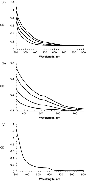 | ||
| Fig. 2 UV-Vis absorption spectra of (a) a quartz substrate bearing 1–4 red NP/C60 coverages on a base layer of PDDA, (b) enlarged visible region of (a), (c) spectrum of red NP in water. | ||
 | ||
| Fig. 3 Atomic force microscopy images of (a) PDDA, (b) PDDA/NP and (c) PDDA/NP/C60 assembled onto a cleaned silicon wafer. Scale: 1 µm × 1 µm. | ||
A simple and informative test to confirm the deposition increments is absorption spectrophotometry. Fig. 2 exemplifies this: the strong band gap transition of the NP chromophore is distinguishable in the visible part of the spectrum (∼500 nm), while the ultraviolet part is dominated by transitions associated with C60 (i.e., 220, 260 and 330 nm). In aqueous solutions of NPs and C60 the same maxima were observed for NP – see Fig. 2. An overall broadening of the spectrum is nevertheless discernable, which can be seen as a spectroscopic signature of electron delocalization due to the strong interaction between individual dyad molecules. Light scattering in the densely packed films could also contribute to the broadening.
In AFM images, the featureless surface with nanometer scale roughness is a typical characteristic of assemblies of polyelectrolyte materials such as PDDA.11 Completely different images were obtained after the subsequent coverage with NP and C60: The roughness of the surface is largely reduced and replaced, on the microscopic level, by fine-grained structures of the NP and C60 layers (Fig. 3) – note the difference in topographic features. While in the case of NP average sizes are of the order of 5–15 nm, for C60, the surface becomes uniformly covered with characteristic 2D aggregates 20–50 nm in size. On the macroscopic level close packing within each NP and C60 layer on top of the PDDA base layer is achieved, as clearly discernable from the AFM images. An important asset is the lack of cluster domains evident on the film surface.
Photocurrents of the modified ITO electrodes were measured under deoxygenated conditions with 1 mM ascorbate/0.1 M NaH2PO4 solutions.12 The major UV-Vis absorber in the NP/PDDA and NP/C60 mixed nanocomposites is the nanoparticle itself. PDDA and C60 are relatively weak absorbers in the region of interest, that is, >350 nm. Thus, not surprisingly, the photoaction spectra of ITO electrodes modified with NP/PDDA or NP/C60 tracks the spectral features that the NPs exhibit in solution and when deposited on quartz – compare Fig. 2 with Fig. 4. Despite this general similarity, a significant difference arises when comparing the photocurrents: a major amplification is seen in those cases where C60 is present – see Figs. 5 and 6. The differences in photocurrent can be as large as 30 and point to the key role of C60 that functions as an electron acceptor and that helps to transform the short-lived photoexcited NP (lifetime 8–22 ns) into a long-lived radical ion pair species (lifetime ≫200 µs). Additionally, we believe that the strong networking features – see TEM experiments – which give rise to notable effects on the electron density also contribute to the high photocurrents.
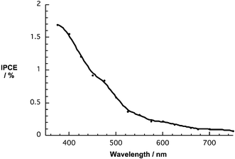 | ||
| Fig. 4 Photoaction spectrum of a modified ITO-electrode bearing a single red NP/C60 coverage on a base layer of PDDA – ITO/PDDA/NP/C60 electrode under deoxygenated conditions (i.e., an aqueous solution containing 0.1 M NaH2PO4 as supporting electrolyte and 50 mM ascorbic acid – no bias voltage applied). Photocurrents were recorded with monochromatic light illumination. | ||
 | ||
| Fig. 5 Layer dependence of photocurrent for ITO/PDDA/{NP/C60}n with n ranging from 1 to 5 under deoxygenated conditions (i.e., an aqueous solution containing 0.1 M NaH2PO4 as supporting electrolyte and 50 mM ascorbic acid – no bias voltage applied). Photocurrents were recorded with light illumination. | ||
 | ||
| Fig. 6 Layer dependence of photocurrent for ITO/PDDA/{NP/PDDA}n with n ranging from 1 to 5 under deoxygenated conditions (i.e., an aqueous solution containing 0.1 M NaH2PO4 as supporting electrolyte and 50 mM ascorbic acid – no bias voltage applied). Photocurrents were recorded with light illumination. | ||
To probe the stability of the photocurrents, an ITO/PDDA/NP/C60 electrode was illuminated over several time intervals. A CuSO4 filter was employed to cut-off the wavelength region that would correspond to the illumination of the ITO electrode itself. Importantly, the response to ON/OFF cycling (i.e., turning the light source on and off) is prompt and reproducible. Over the monitored time window of 60 seconds a moderate decrease in current of less than 5% was noted.
Electrostatic linkage of NP and C60 to the ITO electrode places the primary electron donors, NP, adjacent to the ITO electrode, while the electron acceptor, C60, sits in a remote position relative to the ITO electrode. Thus, within the context of photocurrent generation the following charge transfer scenario develops: initial charge separation within NP/C60 is followed by hole injection into the ITO electrode. Applying a negative bias at the ITO electrode surface is expected to facilitate the hole injection from the one-electron oxidized electron donor (i.e., NP). In fact, changing the bias from +200 mV to 0 mV and to −200 mV vs. Ag/AgCl (0.1 M NaH2PO4, with and without ascorbic acid) leads to a 1.5-fold and a 1.8-fold increase of the photocurrent, respectively.
From the monochromatic light response we calculate an IPCE for an ITO/PDDA/NP/C60 monolayer coverage of 1.7%. Further amplification of the IPCE values were seen for ITO/PDDA/{NP/C60}n – with n ranging from 1 to 5 – yielding the highest IPCE value of 5.4% for n = 5 and the red NP. For orange and green NP ICPE values were as large as 3.0% and 3.5%, respectively.
These numbers are lower than for record-setting solid state devices,13 although exceeding many of them.14 Along with the TiO2-dye charge injection system, the NP·C60 pair sets the example of molecular design for efficient and nearly stable charge separation process – as corroborated in condensed media7 – forming the foundation of any photovoltaic cell. The strategy illustrated here is not optimized, but leaves ample room for potential improvement, which makes possible the surpassing the performance records seen in some of the previously published systems. Electrostatic and van der Waals binding of C60 to NP creates a functional interface, which, subsequently facilitates rapid electron transfer. The versatility of NP chemistry and the LBL deposition process opens up exciting possibilities for further engineering of the redox processes on the electrodes. One of the areas of future research will be acceleration of the charge transport in the film by means of the rational design of multilayer stacks of NP with property gradients.
Acknowledgements
This work was carried out with partial support from the EU (RTN network “WONDERFULL”), MIUR (PRIN 2004, prot. 2004035502), SFB 583, and the Office of Basic Energy Sciences of the U.S. Department of Energy. This is document NDRL-4581 from the Notre Dame Radiation Laboratory.Notes and references
- (a) C. A. Mirkin, MRS Bull., 2001, 26, 535 CAS; (b) N. A. Kotov, MRS Bull., 2001, 26, 992 CAS; (c) H. Coelfen and S. Mann, Angew. Chem., Int. Ed., 2003, 42, 2350 CrossRef.
- (a) E. Pelizzetti and M. Schiavello, Photochemical Conversion and Storage of Solar Energy, Kluwer, Dordrecht, 1997 Search PubMed; (b) J. H. Fendler and I. Dekany, Nanoparticles in Solids and Solutions, Kluwer, Dordrecht, 1996 Search PubMed; (c) P. V. Kamat and D. Meisel, Semiconductor Nanoclusters, Elsevier, Amsterdam, 1997 Search PubMed; (d) J. H. Fendler, Nanoparticle and Nanostructured Films, Wiley-VCH, Weinheim, 1998 Search PubMed.
- (a) H. Imahori and Y. Sakata, Adv. Mater., 1997, 9, 537 CAS; (b) M. Prato, J. Mater. Chem., 1997, 7, 1097 RSC; (c) N. Martin, L. Sanchez, B. Illescas and I. Perez, Chem. Rev., 1998, 98, 2527 CrossRef CAS; (d) H. Imahori and Y. Sakata, Eur. J. Org. Chem., 1999, 2445 CrossRef CAS; (e) F. Diederich and M. Gomez-Lopez, Chem. Soc. Rev., 1999, 28, 263 RSC; (f) D. M. Guldi, Chem. Commun., 2000, 321 RSC; (g) C. A. Reed and R. D. Bolskar, Chem. Rev., 2000, 100, 1075 CrossRef CAS; (h) D. Gust, T. A. Moore and A. L. Moore, J. Photochem. Photobiol., B, 2000, 58, 63 CrossRef CAS; (i) D. M. Guldi and M. Prato, Acc. Chem. Res., 2000, 33, 695 CrossRef CAS; (j) D. Gust, T. A. Moore and A. L. Moore, Acc. Chem. Res., 2001, 34, 40 CrossRef CAS; (k) D. M. Guldi and N. Martin, J. Mater. Chem., 2002, 12, 1978 RSC; (l) D. M. Guldi, Chem. Soc. Rev., 2002, 31, 22 RSC; (m) H. Imahori, Y. Mori and Y. Matano, J. Photochem. Photobiol., C, 2003, 4, 51 CrossRef CAS; (n) J. F. Nierengarten, Top. Curr. Chem., 2003, 228, 87 CAS; (o) D. M. Guldi, Pure Appl. Chem., 2003, 75, 1069 CrossRef CAS; (p) M. E. El-Khouly, O. Ito and F. D'Souza, J. Photochem. Photobiol., C, 2004, 5, 79 CrossRef CAS.
- (a) C. M. Xu, B. Xi, L. Y. Li, C. Wang, S. Wang, Z. Q. Shi, J. H. Fang, S. X. Xiao and D. B. Zhu, New J. Chem., 2001, 25, 1191 RSC; (b) H. Fujihara and H. Nakai, Langmuir, 2001, 17, 6393 CrossRef; (c) P. K. Sudeep, B. I. Ipe, K. G. Thomas, M. V. George, S. Barazzouk, S. Hotchandani and P. V. Kamat, Nano Lett., 2002, 2, 29 CrossRef CAS; (d) Y. S. Shon and H. Choo, Chem. Commun., 2002, 2560 RSC; (e) F. S. Lu, S. Q. Xiao, Y. L. Li, Y. L. Song, H. B. Liu, H. M. Li, J. P. Zhuang, Y. Liu, L. B. Gan and D. B. Zhu, Inorg. Chem. Commun., 2004, 7, 960 CrossRef CAS; (f) C. Roth, I. Hussain, M. Bayati, R. J. Nichols and D. J. Schiffrin, Chem. Commun., 2004, 1532 RSC.
- (a) F. Vögtle, Supramolecular Chemistry, Wiley, Chichester, 1991 Search PubMed; (b) J. M. Lehn, Supramolecular Chemistry – Concepts and Perspectives, VCH, Weinheim, 1995 Search PubMed; (c) J. W. Steed and J. L. Atwood, Supramolecular Chemistry, Wiley, Chichester, 2000 Search PubMed; (d) Comprehensive Supramolecular Chemistry (vols. 1–10), eds. J. L. Atwood, J. E. D. Davies, D. D. MacNicol, F. Vögtle and J.-M. Lehn, Pergamon/Elsevier, Oxford, UK, 1996 Search PubMed; (e) L. F. Lindoy and I. M. Atkinson, Self-Assembly in Supramolecular Systems, Royal Society of Chemistry, Cambridge, UK, 2000 Search PubMed.
- (a) A. L. Rogach, L. Katsikas, A. Kornowski, D. Su, A. Eychmueller and H. Weller, Ber. Bunsen-Ges., 1996, 100, 1772 CAS; (b) M. Gao, A. L. Rogach, A. Kornowski, S. Kirstein, A. Eychmuller, H. Mohwald and H. Weller, J. Phys. Chem. B, 1998, 102, 8360 CrossRef CAS; (c) A. M. Kapitonov, A. P. Stupak, S. V. Gaponenko, E. P. Petrov, A. L. Rogach and A. Eychmuller, J. Phys. Chem. B., 1999, 103, 10109 CrossRef CAS; (d) D. V. Talapin, S. Haubold, A. L. Rogach, A. Kornowski, M. Haase and H. Weller, J. Phys. Chem. B, 2001, 105, 2260 CrossRef CAS.
- D. M. Guldi, I. Zilbermann, G. Anderson, N. A. Kotov, N. Tagmatarchis and M. Prato, J. Am. Chem. Soc., 2004, 126, 14340 CrossRef CAS.
- (a) D. Diaz, J. Robles, T. Ni, S.-E. Castillo-Blum, D. Nagesha, O.-J. A. Fregoso and N. A. Kotov, J. Phys. Chem. B, 1999, 103, 9854 CrossRef CAS; (b) T. Ni, D. K. Nagesha, J. Robles, N. Materer, S. Müssig and N. A. Kotov, J. Am. Chem. Soc., 2002, 124, 3980 CrossRef CAS.
- Leading references: (a) G. Decher, Science, 1997, 277, 1232 CrossRef CAS; (b) P. T. Hammond, Curr. Opin. Colloid Interface Sci., 2000, 46, 430 Search PubMed; (c) M. F. Rubner, Multilayer Thin Films, 2003, 133 Search PubMed; (d) S. W. Keller, S. A. Johnson, E. S. Brigham, E. H. Yonemoto and T. E. Mallouk, J. Am. Chem. Soc., 1995, 117, 12879 CrossRef CAS; (e) X. Zhang and J. Shen, Adv. Mater., 1999, 11, 1139 CrossRef CAS; (f) A. A. Mamedov, A. Belov, M. Giersig, N. N. Mamedova and N. A. Kotov, J. Am. Chem. Soc., 2001, 123, 7738 CrossRef CAS.
- The sequence of operations resulting in production of layered films was the following: (i) dipping of the substrate into a solution of 0.5% PDDA at pH 3 for 10 min, (ii) rinsing with water for 1 min; (iii) dipping of the substrate into a solution of NP at pH 10 for 60 min, (iv) rinsing with water again for 1 min, (v) dipping of the substrate with the NP layer into a solution of C60 at pH 7.2 for 60 min, (vi) final washing for 1 min with water.
- (a) C. Luo, D. M. Guldi, M. Maggini, E. Menna, S. Mondini, N. A. Kotov and M. Prato, Angew. Chem., Int. Ed., 2000, 39, 3905 CrossRef CAS; (b) D. M. Guldi, C. Luo, D. Koktysh, N. A. Kotov, T. Da Ros, S. Bosi and M. Prato, Nano Lett., 2002, 2, 775 CrossRef CAS.
- Photocurrent measurements were carried out using a Keithley model 617 programmable electrometer immediately after illumination. A collimated light beam from a 150 W xenon lamp was used for UV illumination. When white light was used, a CuSO4 cut filter was used. When recording photoaction spectra, a Bausch and Lomb high-intensity grating monochromator was introduced into the path of the excitation beam for selecting the required wavelengths. The incident photon-to-current conversion efficiency (IPCE), defined as the number of electrons collected per incident photon, was evaluated from short circuit photocurrent measurements at different wavelengths versus the photocurrent measured using a photodiode of the type PIN UV 100 (UDT Sensors Inc.).
- (a) W. U. Huynh, J. J. Dittmer and A. P. Alivisatos, Science, 2002, 295, 2425 CrossRef CAS; (b) T. Stergiopoulos, I. M. Arabatzis, H. Cachet and P. Falaras, J. Photochem. Photobiol., A, 2003, 155, 163 CrossRef CAS; (c) H. van't Spijker, B. O'Regan and A. Goossens, J. Phys. Chem. B, 2001, 105, 7220 CrossRef CAS; (d) N. S. Lewis, Nature, 1983, 305, 671 CrossRef; (e) M. Graetzel, Nature, 2001, 414, 338 CrossRef CAS; (f) N. S. Sariciftci, L. Smilowitz, A. J. Heeger and F. Wudl, Science, 1992, 258, 1474 CrossRef CAS; (g) L. Schmidt-Mende, A. Fechtenkotter, K. Mullen, E. Moons, R. H. Friend and J. D. MacKenzie, Science, 2001, 293, 1119 CrossRef CAS.
- C. L. Huisman, A. Goossens and J. Schoonman, Synth. Met., 2003, 138, 237 CrossRef CAS.
| This journal is © The Royal Society of Chemistry 2005 |