Integrated circuit/microfluidic chip to programmably trap and move cells and droplets with dielectrophoresis†‡
Thomas P.
Hunt
a,
David
Issadore
b and
R. M.
Westervelt
*ab
aDepartment of Physics, Harvard University, 29 Oxford Street, Cambridge, MA 02138, USA
bSchool of Engineering and Applied Science, Harvard University, 29 Oxford Street, Cambridge, MA 02138, USA. E-mail: westervelt@seas.harvard.edu
First published on 2nd November 2007
Abstract
We present an integrated circuit/microfluidic chip that traps and moves individual living biological cells and chemical droplets along programmable paths using dielectrophoresis (DEP). Our chip combines the biocompatibility of microfluidics with the programmability and complexity of integrated circuits (ICs). The chip is capable of simultaneously and independently controlling the location of thousands of dielectric objects, such as cells and chemical droplets. The chip consists of an array of 128 × 256 pixels, 11 × 11 µm2 in size, controlled by built-in SRAM memory; each pixel can be energized by a radio frequency (RF) voltage of up to 5 Vpp. The IC was built in a commercial foundry and the microfluidic chamber was fabricated on its top surface at Harvard. Using this hybrid chip, we have moved yeast and mammalian cells through a microfluidic chamber at speeds up to 30 µm sec–1. Thousands of cells can be individually trapped and simultaneously positioned in controlled patterns. The chip can trap and move pL droplets of water in oil, split one droplet into two, and mix two droplets into one. Our IC/microfluidic chip provides a versatile platform to trap and move large numbers of cells and fluid droplets individually for lab-on-a-chip applications.
Introduction
Automated handling of fluid and biological samples has played an enabling role in the growing fields of drug discovery, genetic sequencing and synthesis, cell sorting, and single cell gene expression studies.1–3 The continuing effort to manipulate increasingly large sets of diminishingly small objects has led to a technological push for miniaturization and automation in fluid handling.4–8At the forefront of miniaturized tools to interact with biological samples and fluids is the fast-growing field of microfluidics,1–7 which has allowed researchers to control and analyze sub-µL fluid volumes using fabricated µm-scale pipes and valves. This paradigm shift in biotechnology is analogous to that which the semiconductor industry faced half of a century ago, culminating in the integrated circuit (IC).8
The addition of electronics to microfluidic systems can provide enhanced capabilities.8–13 Sensitive detectors, electrical manipulation techniques and fast, programmable logic can be directly integrated into an electronic/microfluidic chip.8,9,13 In an electronic/microfluidic system, the path of fluid elements and particles need not be limited to a fixed channel geometry.8–13 Programmable microfluidic systems for droplet manipulation with electrowetting (EW)10,11 and dielectrophoresis (DEP)12,13 were initially developed with external control electronics. DEP has been used to manipulate nanoparticles,14 viruses15 and single molecules.16 Combining ICs and microfluidics in a single chip allows even more functionality: systems for magnetic manipulation,17 recording and stimulating electrogenic cells18,19, dielectric manipulation and sensing,9,20 and DNA detection21 have all been developed.
The focus of our research is to use the existing technology and infrastructure of the semiconductor industry to build devices for the manipulation of biological samples and fluid droplets for biology and medicine. In this article, we report the development and testing of a hybrid IC/microfluidic chip that moves cells and small fluid droplets inside a microfluidic chamber using DEP, the forced motion of dielectrics in non-uniform electric fields. The chip can trap and move many biological cells or small volumes of fluid independently; imaging is provided by an optical microscope. This microfluidic system can be dynamically programmed to carry out sorting or assembly processes, and it can react to features recognized in the optical images.
Manaresi et al.9 developed an IC/microfluidic DEP chip for the programmable manipulation and detection of cells using a 320 × 320 array of 20 × 20 µm2 pixels. The IC/microfluidic chip presented in this article contains a 128 × 256 array of 11 × 11 µm2 pixels that can trap and move cells or liquid droplets in a microfluidic chamber using DEP. An image of the energized pixels is stored in SRAM immediately below the pixel array. Electric field gradients are created by applying an actuation voltage of up to 5 V between neighboring pixels. Fine pixel spacing enhances the field gradient between pixels and allows for improved control over the position of single cells. Large field gradients produced by our chip create strong DEP forces that are capable of moving cells at speeds of up to 30 µm sec–1, three times faster than the chip used in ref. 9.
Our IC/microfluidic chip can also trap and move very small liquid droplets along programmed paths. Previous microfluidic devices10–13 have manipulated liquid drops using EW and DEP. Our chip can move droplets using only 5 V, much lower than the voltages required for previous chips.10–13 Low voltage droplet manipulation is possible because the droplets on the chip are suspended at the boundary between a layer of low-density oil and a layer high-density oil that prevents the drop from coming into contact with the chip's surface, eliminating contact line hysteresis as a source of drag. Only fluidic drag must be overcome in order to move droplets, and our chip can move them at speeds of up to ∼5 µm sec–1 with only 5 V between pixels. Because high voltages are not required, a standard complementary metal oxide semiconductor (CMOS) process can be used to fabricate our chips, allowing smaller pixel size, correspondingly reduced droplet size, and decreased cost.
We present a hybrid IC/microfluidic system that consists of a microfluidic chamber built on top of a custom IC manufactured in a foundry. The IC has a two-dimensional array of pixels with integrated SRAM memory elements, similar in architecture to a computer display or a CCD (Fig. 1). In our device, each pixel is individually driven with a radio frequency (RF) voltage, creating a local electric field that exerts a force via DEP on a cell or fluid droplet in the microfluidic chamber above the IC's surface. Programmed micro-patterned, time-dependent RF electric fields can be formed and used to trap and move objects in fluids above the IC.
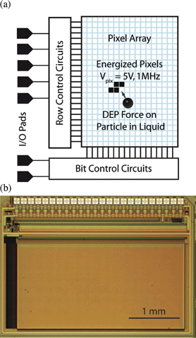 | ||
| Fig. 1 (a) DEP manipulator IC block diagram; (b) optical micrograph of the DEP IC. | ||
The IC was designed and built using a standard CMOS design and lithographic process. The chip consists of a 1.4 × 2.8 mm2 array of 32![[thin space (1/6-em)]](https://www.rsc.org/images/entities/char_2009.gif) 768 individually addressable 11 × 11 µm2 pixels. An RF voltage with an amplitude of 5 Vpp at frequencies from DC to 1.8 MHz can be applied to each pixel, producing a localized electric field nearby to trap a cell or a droplet of fluid. A microfluidic chamber was fabricated on the top surface of the IC using the Center for Nanoscale Systems’ facilities at Harvard.
768 individually addressable 11 × 11 µm2 pixels. An RF voltage with an amplitude of 5 Vpp at frequencies from DC to 1.8 MHz can be applied to each pixel, producing a localized electric field nearby to trap a cell or a droplet of fluid. A microfluidic chamber was fabricated on the top surface of the IC using the Center for Nanoscale Systems’ facilities at Harvard.
After describing the design and fabrication of the chip, we now demonstrate how it can be programmed to trap and move individual yeast and mammalian cells in solution. We show how thousands of individual yeast cells can be trapped and simultaneously positioned into controlled patterns. The chip can also be used to trap, move and manipulate droplets of fluid. We show examples of the chip translating pL droplets of water in oil, splitting one droplet into two and mixing two droplets into one.
Dielectrophoresis theory
Dielectrophoresis is the motion of a dielectric object in a non-uniform electric field. A non-uniform electric field creates an induced electric dipole in a dielectric that feels a force in the non-uniform field. By applying an appropriate local electric field pattern, any particle with a dielectric constant different to that of the surrounding medium can be manipulated with DEP. The DEP force on a spherical particle is:22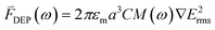 | (1) |
 is the medium permittivity and CM(ω) is the Clausius–Mossotti factor, a relation between the frequency-dependent complex permittivity of the particle and the medium;
  and
and  are the complex permittivity of the particle and medium, respectively.
 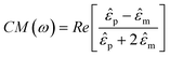 | (2) |
The Clausius–Mossoti factor, CM(ω), can vary between –0.5 and 1, with important physical implications. When CM(ω) < 0, the fluid is more polarizable than the particle and the particle is pulled towards the local minimum of the electric field; this is called negative DEP (nDEP). Positive DEP (pDEP) (CM(ω) > 0) occurs when the particle is more polarizable than the fluid and the particle is pulled to the maximum of the electric field.
The hybrid chip in this paper uses pDEP to move cells and droplets in the experiments described. By shifting the location of the energized pixels, the array changes the location of the local electric field maxima, trapping and moving cells along programmable paths through the microfluidic chamber. In both model and experiment, it was not necessary to use a conductive coverslip for cell and droplet manipulation. Our system was equally capable of nDEP manipulation, with confinement in the Z-direction perpendicular to the chip provided by gravity or a coverslip.
Methods
Integrated circuit architecture
The chip consists of an array of 128 × 256 pixels surrounded by circuitry to address and control the pixels, as shown in Fig. 1(a). The Row Control Circuits in Fig. 1(a) select a row of pixels and the Bit Control Circuits select a column, allowing individual pixels to be addressed. Each pixel contains a memory element that stores its state. An optical micrograph of the integrated circuit is shown in Fig. 1(b).We selected a 0.35 µm gate length CMOS process with four metal layers, and 5 V transistors, that is available through MOSIS (process: TSMC35_P2). The process was chosen to provide strong field gradients for DEP, and a pixel size that matched cellular size scales of ∼10 µm. A summary of the IC design parameters is shown in Table 1.
| Process | 0.35 µm, CMOS MOSIS TSMC35_P2 |
| Pixels | 128 × 256 (32768) 11 × 11 µm2 pixels |
| Chip size | 2.32 × 3.27 mm2 |
| Addressing | 8-bit word line decoder; 128-bit, two-phase clocked shift register for bit lines |
| Transistor count | ∼360000 |
| Pixel voltage | V pix = 3 to 5 V, DC to 1.8 MHz |
| Operating current | 30 to 100 mA |
The circuit diagram of a single pixel in the hybrid chip is shown in Fig. 2(a). Each pixel consists of three basic circuit blocks: (1) a static random access memory (SRAM) element to store the state of the pixel, (2) control transistors that, depending on the state of the SRAM, allow an RF voltage of either Vpix or the logical inverse ![[V with combining macron]](https://www.rsc.org/images/entities/i_char_0056_0304.gif) pix to be applied to the DEP electrode and (3) drive transistors to pull-up and pull-down the capacitive load of the pixel.
pix to be applied to the DEP electrode and (3) drive transistors to pull-up and pull-down the capacitive load of the pixel.
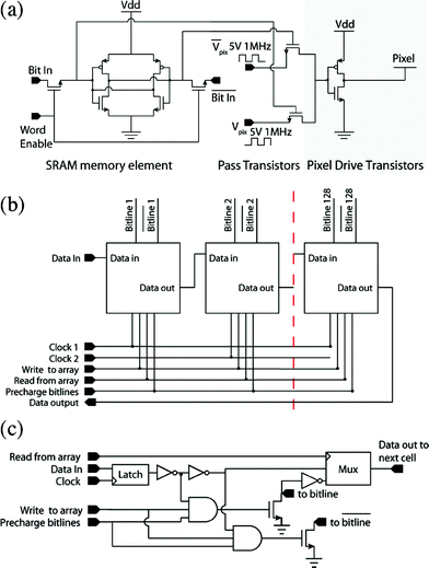 | ||
| Fig. 2 (a) DEP manipulator pixel schematic diagram. The circuit consists of three major parts, an SRAM memory element, pass transistors and an inverter to drive the pixel. The state of the SRAM selects a pass transistor, which sends Vpix or pix to the pixel drive transistors. (b) Bit line control circuit block diagram. The dashed line represents blocks that serve bit line 3 to bit line 127. (c) Schematic of 1 of the 128 bit line control cells. | ||
The RF voltage Vpix and its inverse pix are signals that are created off the chip. Vpix is an RF square wave with a 50% duty cycle and a frequency that can range from DC to 1.8 MHz. The memory element of each pixel determines whether the pixel is driven with Vpix or pix. There are several advantages to driving pixels with either Vpix or its inverse pix rather than Vpix or a DC value. The electric field between two adjacent pixels held at Vpix and pix time-averages to zero, so there is no electrophoresis of charged particles in the microfluidic system. For AC actuation, the RMS electric field between Vpix and pix is twice the RMS electric field attainable between Vpix and ground, providing a greater DEP force.
The time taken for the pixel voltage to ramp up or down is short compared to the period of Vpix. The transistors that drive each pixel have an on-resistance of approximately 10 kΩ, and they drive a pixel capacitance of less than 50 fF, yielding a sub-nS resistance × capacitance (RC) time.
To maximize the pixel density of the IC, we minimized the number of transistors under each pixel and optimized the circuit layout to pack transistors as densely as possible. To further conserve chip area, all the PMOS transistors for pixels on a common word line shared an N-doping well.
All bond pads are located on one side of the chip, facilitating the fabrication of the microfluidic system. Input/output (IO) pads were designed to provide 1.6 kV electrostatic discharge (ESD) protection without consuming excessive chip area.
Logic design
To individually address the 128 × 256 pixels in the array, circuits are used to selectively update the pixel states according to their row and column. A decoder is used that identifies each row with a unique 8-digit binary number. The state of each of the 128 pixels in a row are loaded sequentially into a shift register, as shown in Fig. 2(b), and simultaneously written to the designated row.The shift register is updated using a 2-phase clocking scheme with Clock1 and Clock2. Control signals Read and Write determine whether the bits in a row are written from the shift register or are read. The memory states are written using a 2-phase, clocked, pre-charged logic. The schematic of each element of the shift register is shown in Fig. 2(c).
To set the pixel values of one word of pixels on the chip, data for each pixel are loaded into a two-phase clocked shift register. Bitline pre-charging is disabled, the write to array signal is given, and the bitlines corresponding to the data in each latch are pulled down by NMOS transistors. An 8-bit word line decoder enables one of the 256-word lines on the chip to be written, and the bitline values are written to the SRAM elements on the selected word.
To non-destructively read the SRAM memory elements on the chip and confirm which pixels are energized, bitline pre-charging is disabled, a wordline is enabled and all the bits of the selected word are read to the 128 latches. Subsequent 2-phase clocking steps the latch values through the final latch to an output amplifier (digital inverter, output current 10 µA) and on to an output pin.
Electric field simulations
In Fig. 3, we show simulations of the electric field magnitude |E| and the force field F for an 8 µm diameter sphere above the chip with the dielectric properties of a cell in a water bath. The simulation geometry was modelled on an actual chip geometry of 10.4 × 10.4 µm2 metal pixels with a 0.6 µm spacing in either direction, capped with a 3 µm thick polyimide layer, beneath a 200 µm deep microfluidic chamber filled with water. In the simulation, two pixels were set to 5 V, leaving all the other pixels at ground (Fig. 3(a)). Finite element simulations were used to determine the electric field |E| (Fig. 3(b)), from which the DEP forces F were calculated (Fig. 3(c)). The simulations were executed using Maxwell 3D (Ansoft Inc.).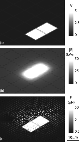 | ||
| Fig. 3 Finite element simulations of fields produced by the CMOS/microfluidic chip. (a) Electric potential of two energized pixels. (b) Resulting electric field magnitude 4 µm above the surface of the chip. (c) DEP force in the x–y plane acting on an 8 µm diameter cell in the microfluidic channel. | ||
The simulations showed that a cell in the microfluidic channel was exposed to a maximum electric field of ∼50 kV m–1, and that an 8 µm diameter cell above one electrode would be subject to a DEP force of approximately 5 pN when a neighbouring electrode was energized.
Microfluidic packaging
The microfluidic packaging scheme is shown in Fig. 4. IC dies were received from the foundry, and all subsequent processing was done using the Center for Nanoscale Systems’ facilities at Harvard. We first mounted the IC on a copper block for heat transfer, then wirebonded the IC to microfabricated leads. Our microfluidic channel was cut out of a layer of hot-melt adhesive. With hot-melt channel walls, we were able to remove the entire microfluidic system to clean the IC surface by moderately heating the chip and peeling off the channel layer.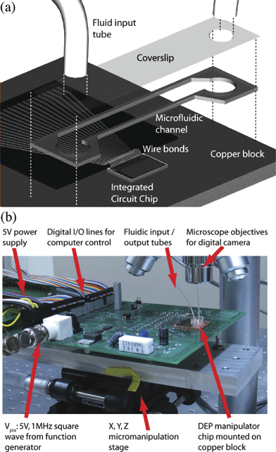 | ||
| Fig. 4 (a) IC/microfluidic chip packaging scheme. The IC is mounted on a copper block and wirebonded to electrical leads. A hot-melt microfluidic channel is bonded to the IC and copper block, and a drilled coverslip sealed on top. Fluid enters through the holes in the coverslip. (b) IC/microfluidic DEP chip experimental setup. | ||
In detail, the fluid channel walls were formed by casting adhesive between silanized glass slides on a hotplate at 100 °C. We peeled off the thin layer of adhesive and cut out the microfluidic channel with a hole punch (Harris Uni-core, Pella Inc.). Under a binocular dissecting microscope, we aligned the microfluidic channel onto the IC surface while heating the chip to approximately 90 °C.
Two schemes were used to introduce fluid into the channel. The microfluidic channel could be filled by pipette with a few µL of liquid and sealed by a coverslip placed on top. Alternatively, we could thermally bond a coverslip with drilled holes to the hot-melt microfluidic channel. We could inject fluid with a syringe pump into the microfluidic channel through the holes in the coverslip. We chose to use simple microfluidic chambers to demonstrate the programmable nature of the chip. To carry out a specific application, additional microfluidic systems could be constructed on the top side of the coverslip to supply reagents, cells and fluid drops in a controlled way to the microfluidic chamber above the IC.
Interface and software design
To control and program the hybrid chip, the IC is electrically connected to a computer. Control signals were sent to a custom printed circuit board (PCB) by a National Instruments PCI-6254 card in the computer. The RF voltage, Vpix, is provided by a function generator, andpix by an inverter on the PCB. The computer runs a custom user interface written in Igor Pro (Wavemetrics, Inc.), with NI-DAQ software to send signals to the PCB. The PCB also has RC filters to protect the input to the IC. The PCB was designed using PCAD (Altium, Ltd.) in the Harvard Electronics Shop, and manufactured by Advanced Circuits.
The IC was designed for a 1 MHz pixel read and write rate. However, the control board had a limited update rate of approximately 20 kHz. This I/O speed allowed a word of 128 pixels to be updated at ∼100 Hz, which was adequate for our experiments.
Experimental setup
Fig. 4(b) shows the IC/microfluidic DEP manipulator chip experimental setup. The PCB containing the hybrid chip was mounted on a microscope stage. Wirebonds connect the electrical leads to the circuit board and are protected from fluid and mechanical damage by a layer of PDMS. The motion of manipulated cells and droplets in the microfluidic chamber was visualized and recorded using an optical microscope with a CCD camera.Results
Yeast manipulation with the IC/microfluidic chip
In this section, we demonstrate how the hybrid chip can be programmed to trap and move individual yeast and mammalian cells in solution. Yeast cells were cultured overnight in YPD broth (BD Inc.) at 37 °C. The conductivity of the broth was approximately 1 S m–1, as measured by an Orion 116 conductivity meter (Thermoelectron Inc). We re-suspended the yeast in a mannitol buffer, with a conductivity of 100 µS m–1, to reduce the effects of heating and electrohydrodynamic flow in the strong electric fields produced by the DEP chip. Approximately 5 µL of yeast cells in mannitol were pipetted onto the chip.
Fig. 5a shows microscope images of three yeast cells that are trapped and moved by the chip. At 0 seconds, a set of pixels were energized with Vpix to trap three yeast cells above the pixel array, while all of the other pixels were held at pix. By moving the location of energized pixels, the 3 cells were individually moved from one pixel to a neighboring pixel at a speed ∼30 µm sec–1. After 4 sec, two of the yeast cells were moved to join the third cell, as indicated by the black arrows in Fig. 5a. Using this technique, It was possible to move a cell along an arbitrary path by energizing a sequence of pixels. It was also possible to separate two neighbouring cells by switching the pixels beside them. Information gained from optical images of the cells during an experiment can be used to change the excitation of pixels to move two cells along different paths, to sort cells based on cell type.
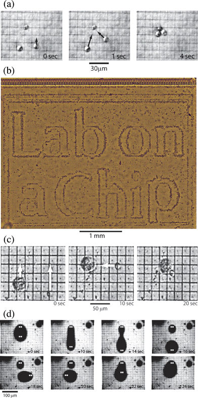 | ||
| Fig. 5 (a) Time sequence of the DEP manipulation of yeast cells. Pixels are energized in sequence to move first one cell alone and then all three together. The maximum speed of a yeast cell was approximately 30 µm sec–1. (b) Complex pattern of thousands of yeast cells patterned by DEP. Pixels across the array were energized to spell out “Lab on a Chip”, attracting cells toward the local maxima of the electric field. (c) Time sequence of yeast and rat alveolar macrophages manipulated with DEP. Pixels on the chip were energized to independently move the two cells and then bring them together. (d) Splitting, moving and combining water drops in oil with DEP. This time sequence shows a droplet of dyed water between a layer of fluorocarbon oil below and hydrocarbon oil above. The pixels energized with Vpix in each frame are highlighted in white. | ||
By appropriately addressing the pixel array, we could simultaneously trap and move thousands of individual cells. Fig. 5(b) shows yeast cells that have been moved to form a pattern programmed by the DEP array. First, the pixels were energized in a bitmap to spell “Lab on a Chip”. Next, yeast cells in mannitol were pipetted onto the chip surface. As the cells sedimented, they were attracted to the local maxima in the electric field produced by the pattern of energized pixels on the chip surface. The image was taken once the cells had settled in the fluid at the surface of the chip ∼10 min after introducing the yeast suspension. The electric fields produced by the energized pixels are highly localized and only pull cells in from a distance of ∼50 µm. Some cells visible in Fig. 5(b) settled in regions far from any energized pixels, but these cells can be individually moved toward any desired location by energizing a sequence of pixels, as in Fig. 5(a). The programmable patterning of large numbers of cells could have applications in the assembly of tissue.
In addition to yeast cells, we manipulated mammalian cells, as shown in Fig. 5(c). Rat alveolar macrophages were prepared in the Bioimaging Lab at the Harvard School of Public Health. The cells were obtained by bronchoalveolar lavage and suspended in a low conductivity buffer, 0.1 M sucrose, to avoid heating and electrohydrodynamic (EHD) flow. Residual ions brought the conductivity of the sucrose buffer to 100 µS m–1. We were able to trap and move rat alveolar macrophages in the same manner that we used to move yeast cells. To demonstrate the potential of our chip to assemble tissue from multiple cell types and to enable studies of cell–cell interactions, we simultaneously moved both rat alveolar macrophages and yeast cells, as shown in Fig. 5(c). We were able to deliver multiple yeast cells to the surface of a rat alveolar macrophage, as well as control the distance between cells of different types.
Droplet manipulation
In this section, we describe how the DEP manipulator chip can be used to move, split and combine droplets of water in oil. Water droplets with volumes ranging from ∼1 pL to ∼1 nL were programmably manipulated by the electric fields produced by the chip. Fig. 5(d) shows the DEP manipulation of dyed water drops in oil, with the energized pixels highlighted in white. Droplets were deformed by energizing multiple sets of pixels. Holding a droplet in place with two energized pixels, another set of pixels was energized to stretch the droplet. As it was stretched, the single droplet elongated and pinched in the middle to form two separate droplets. Both resulting droplets could be moved independently. The droplets recombined when they were brought into contact.To prepare drops for manipulation, a mixture of hexadecane, water and sodium dodecyl sulfate (SDS) surfactant was shaken using a vortexer. A thin layer of fluorocarbon oil was pipetted onto the surface of the chip, and then the suspension of water drops in hexadecane was added to the microfluidic channel. The difference in density among the three liquids resulted in water drops (η = 1 g cm–3) that were pinched between a layer of dense fluorocarbon oil (η = 2.4 g cm–3) and less dense hexadecane (η = 0.8 g cm–3). The multi-layer liquid provided very little resistance to the translating drops in a plane above the surface of the chip. The drops were not in contact with the chip surface, and so it was not necessary to overcome contact line hysteresis to move them. In addition, droplet manipulation was insensitive to the surface treatment and hydrophobicity of the chip.
The control of droplets of aqueous chemicals in oil is a major accomplishment for our IC/microfluidic system. Unlike other DEP and EW chips, which manipulate drops with tens or hundreds of volts, our chip is capable of manipulating drops with 5 V, allowing the use of a standard 5 V CMOS process.
IC/microfluidic systems capable of droplet manipulation could serve as a platform for programmable, automated chemistry. Reservoirs of chemicals along the edge of the chip could be used to deliver fluid droplets, pinched off by DEP, and mixed together in any programmable pattern to perform a wide variety of biochemical assays. The chip offers the possibility of deforming a droplet using DEP and mixing the contents faster than simple diffusive mixing. In addition, programmable control of droplets allows pL chemical doses to be delivered directly to droplets that contain single cells, so as to observe their effects.
Discussion
DEP field frequency and biocompatibility
There are several reasons to use AC fields in our DEP chip. AC fields allow us to avoid ion shielding of the electrodes. In a conductive medium, AC fields of sufficient frequency (>10 kHz) do not suffer from ionic screening or electrode polarization, i.e. ions cannot move fast enough to screen the applied field. The movement of particles due to net charge (electrophoresis) will time-average to zero in an AC field, and electroosmotic flow of the double layer along liquid–solid boundaries is eliminated. Another benefit of AC fields is that they are less harmful to cells, because the voltage across the capacitive membrane of the cell is less than that with a DC field.We calculate that a cell on our DEP chip experiences a maximum transmembrane voltage of ∼30 mV due to the applied electric field of 50 kV m–1 at 1 MHz. A number of studies have shown that cells subject to less than 105 V m–1 at frequencies greater than 1 MHz show few signs of damage due to the applied electric field.23
Dielectrophoresis chip scaling
Our chip was constructed using a 0.35 µm, 5 V CMOS process as a compromise between expense, pixel size and actuation voltage. The 0.35 µm gate width is several generations behind current CMOS technology. Intel has demonstrated a 0.57 µm2SRAM in their 65 nm production process.24 A DEP chip with an identical architecture to our current chip requires only four transistors per pixel, in addition to the basic SRAM building block. As a result of progress in the semiconductor industry, it is straightforward to design DEP pixels with a size of 1 × 1 µm2 instead of 11 × 11 µm2.An unfortunate consequence of semiconductor scaling is that smaller transistors have a lower breakdown voltage. The semiconductor industry has purposefully pursued lower voltages to maximize switching speed whilst minimizing power dissipation, using 0.9 to 1.2 V power supplies for the 65 nm processes. With slight modifications, specifically a thicker gate oxide, we can sacrifice switching speed for increased gate-source voltage. The source-drain breakdown voltage can also be increased by adding a lightly doped drift region to each transistor.25 Even without process modification, a DEP chip fabricated with a 65 nm, 1 V CMOS process would produce strong electric fields and field gradients for DEP due to the short separation between pixels. The passivation thickness above the metal layers must scale with the pixel size, or the field gradient used for DEP will fall off within the passivation.
Small DEP manipulator chips constructed with cutting edge semiconductor technology could be very useful for positioning nanoparticles in complex patterns. Post-processing with nanolithography, such as electron beam lithography, could be useful in applying this approach to the nanoscale.
Conclusions
Combining the sensitivity and programmability of ICs with the biocompatibility of microfluidics, IC/microfluidic chips have the potential to make a major impact on biomedical research. Our IC/microfluidic DEP manipulator chip is capable of moving pL chemical volumes and large numbers of individual cells. With ICs becoming more powerful each year and microfluidics beginning to enter the commercial arena, IC/microfluidic chips are poised to take advantage of advances in both industries.Acknowledgements
We would like to thank the National Cancer Institute MIT-Harvard CCNE, and the Nanoscale Science and Engineering Center (NSEC) at Harvard under NSF grant PHY-0117795 for funding. We also thank Professor Donhee Ham for graciously allowing us access to chip design software and Maxwell 3D (donated by Ansoft). Thanks go to Dr Rick Rodgers and Dr Rosalinda Sepulvda at the Harvard School of Public Health for providing mammalian cells.References
- G. M. Whitesides, E. Ostuni, S. Takayama, X. Jiang and D. Ingber, Ann. Rev. Biomed. Eng., 2001, 3, 335 CrossRef CAS and references therein.
- H. A. Stone, A. D. Stroock and A. Ajdari, Ann. Rev. Fluid Mech., 2005, 36, 381 Search PubMed and references therein.
- P. Tabeling, Introduction to Microfluidics, Oxford University Press, New York, 2005, and references therein Search PubMed.
- J. Han, S. W. Turner and H. G. Craighead, Phys. Rev. Lett., 1999, 83, 1688 CrossRef CAS.
- T. Thorsen, S. J. Maerkl and S. R. Quake, Science, 2002, 298, 580 CrossRef CAS.
- R. G. Blazej, P. Kumaresan and R. A. Mathies, Proc. Natl. Acad. Sci. U. S. A., 2006, 103, 7240 CrossRef CAS.
- G. M. Whitesides, Nature, 2006, 442, 368 CrossRef CAS.
- CMOS Biotechnology, ed. H. Lee, D. Ham and R. M. Westervelt, Springer, New York, 2007 and references therein Search PubMed.
- N. Manaresi, A. Romani, G. Medoro, L. Altomare, A. Leonardi, M. Tartagni and R. Guerrieri, IEEE J. Solid-State Circuits, 2003, 38, 2297 CrossRef.
- J. Lee, H. Moon, J. Fowler, T. Schoellhammer and C. J. Kim, Sens. Actuators, A, 2002, 95, 259 CrossRef.
- M. G. Pollack, A. D. Shendorov and R. B. Fair, Lab Chip, 2002, 2, 96 RSC.
- J. Vykoukal, A. Schwartz, F. F. Becker and P. R. C. Gascoyne, in Micro Total Analysis Systems, ed. J. M. Ramsey and A. van den Berg, Kluwer, Dordrecht, 2001, pp. 72 Search PubMed.
- P. R. C. Gascoyne, J. V. Vykoukal, J. A. Schwartz, T. J. Anderson, D. M. Vykoukal, K. W. Current, C. McConaghy, F. F. Becker and C. Andrews, Lab Chip, 2004, 4, 299 RSC.
- N. G. Green and H. Morgan, J. Phys. D: Appl. Phys., 1997, 30(11), L41 CrossRef CAS.
- N. G. Green, H. Morgan and J. J. Milner, J. Biochem. Biophys. Methods, 1997, 35, 89 CrossRef CAS.
- R. Hölzel, N. Calander, Z. Chiragwandi, M. Willander and F. Bier, Phys. Rev. Lett., 2005, 95, 128102 CrossRef.
- H. Lee, Y. Liu, R. M. Westervelt and D. Ham, IEEE J. Solid-State Circuits, 2006, 41, 1471 CrossRef.
- B. D. DeBusschere and G. T. A. Kovacs, Biosens. Bioelectron., 2001, 16, 543 CrossRef CAS.
- B. Eversmann, M. Jenkner, F. Hofmann, C. Paulus, R. Brederlow, B. Holzapfl, P. Fromherz, M. Merz, M. Brenner, M. Schreiter, R. Gabl, K. Plehnert, M. Steinhauser, G. Eckstein, D. Schmitt-Landsiedel and R. Thewes, IEEE J. Solid-State Circuits, 2003, 38, 2306 CrossRef.
- K. Current, K. Yuk, C. McConaghy, P. Gascoyne, J. Schwartz, J. Vykoukal and C. Andrews, IEEE Symp. VLSI Circuits Digest, 2005, 72 Search PubMed.
- R. Thewes, F. Hofmann, A. Frey, B. Holzapfl, M. Schienle, C. Paulus, P. Schindler, G. Eckstein, C. Kassel, M. Stanzel, R. Hintsche, E. Nebling, J. Albers, J. Hassman, J. Schulein, W. Goemann and W. Gumbrecht, IEEE Int. Conf. Solid-State Circuits: Digest of Technical Papers, 2002, 1, 350 Search PubMed.
- T. B. Jones, Electromechanics of Particles, Cambridge University Press, Cambridge, 1995 Search PubMed.
- C. Grosse and H. Schwan, Biophys. J., 1992, 63, 1632 CrossRef CAS.
- K. Zhang, U. Bhattacharya, Z. Chen, F. Hamzaoglu, D. Murray, N. Vallepalli, Y. Wang and M. Bohr, IEEE J. Solid-State Circuits, 2005, 40, 895 CrossRef.
- H. Ballan and M. Declercq, High Voltage Devices and Circuits in Standard CMOS Technologies, Kluwer, Dordrecht, 1999 Search PubMed.
Footnotes |
| † The HTML version of this article has been enhanced with colour images. |
| ‡ Electronic supplementary information (ESI) available: Cell and droplet manipulation movies. See DOI: 10.1039/b710928h |
| This journal is © The Royal Society of Chemistry 2008 |