Surface properties of SnO2nanowires for enhanced performance with dye-sensitized solar cells†
Suresh
Gubbala
a,
Harry B.
Russell
a,
Hemant
Shah
b,
Biswapriya
Deb
d,
Jacek
Jasinski
d,
Heather
Rypkema
c and
Mahendra K.
Sunkara
*a
aDepartment of Chemical Engineering, University of Louisville, Louisville, KY 40292. E-mail: mahendra@louisville.edu
bDepartment of Electrical and Computer Engineering, University of Louisville, Louisville, KY 40292
cDepartment of Chemistry, University of Louisville, Louisville, KY 40292
dInstitute for Advanced Materials and Renewable Energy, University of Louisville, Louisville, KY 40292
First published on 22nd September 2009
Abstract
Our recent studies showed that nanowire based DSSCs exhibited over 250 mV higher open circuit potentials (VOC) compared to those using nanoparticles. In this study, the electron transport and surface properties of nanowires and nanoparticles are investigated to understand the reasons for the observed higher photovoltages with NW based solar cells. It was seen that, in addition to slow recombination kinetics, the lower work function of SnO2nanowires compared to the nanoparticle counterparts also significantly contributes to the high VOC observed for the nanowire based DSSCs.
Broader contextDye sensitized solar cell technology has the potential to bring down cost per watt to meet the terawatt challenge using solar energy conversion. Titania nanoparticle films have been a widely used anode material for these types of cells, but suffer from high recombination losses and low electron transport properties. So, new materials and architectures are sought to further improve the performance of DSSCs. Many studies have been done, which have primarily focused on one-dimensional TiO2 and ZnO2 materials as the alternate materials, but have seen no improvement in the DSSC performance over their nanoparticle counterparts. In the past, we had suggested and explored the possibility of using SnO2nanowires for DSSCs. Our previous study suggested that the nanowires exhibit superior characteristics over nanoparticles in DSSCs in terms of transport and recombination properties and surprisingly with higher photovoltages. So, in this study, we used a number of tools and techniques to understand the surface and electronic properties of both tin oxide nanowires and nanoparticles. The results showed that lower work function, two orders of magnitude higher recombination time scales and an order of magnitude improvement in transport time scales have all contributed to the 200–250 mV higher photovoltages observed with nanowires over nanoparticles in DSSCs. |
Introduction
Tin oxide is a widely available, large bandgap material, with appropriate band edges for use as the anode material in dye sensitized solar cells (DSSCs). In addition, due to its large bandgap, it is more stable against UV degradation.1 So, there has been large interest in studying the properties of SnO2 based materials in DSSCs.2,3 However, the open circuit potentials for SnO2nanoparticle-based DSSCs have been observed to be much less than 400 mV, making them less attractive as anode materials for DSSCs. Typically, the VOC values for SnO2nanoparticle based DSSCs are on the order of only 300 mV but vary over a wide range (>250 and <400 mV).4–8 The observed low open circuit potentials have been attributed to high recombination kinetics with the electrolyte.9Recently, our work showed that DSSCs based on tin oxide nanowires exhibited high open circuit voltages (520–560 mV), faster electron transport and slower electron recombination characteristics compared to tin oxide nanoparticle counterparts.10 However, in the above stated study, many questions remained unanswered regarding the origin of the differences between nanowire and nanoparticle based systems. One main question was, whether the higher VOC of nanowire based DSSCs was due to a difference in their work functions or due to slower electron recombination characteristics in nanowires compared to nanoparticles. In addition, it was not clear why slow recombination kinetics were observed with nanowires compared to nanoparticles when both materials were stoichiometric tin oxide. It has been observed in many nanoparticle systems that recombination kinetics increase with faster electron transport.11 This, however has been found to be different in the case of one dimensional materials like zinc oxide nanowires, in which faster transport did not have any effect on the recombination kinetics.12
In this study, the surface composition and electronic properties of both nanowires and nanoparticles are investigated and are discussed within the context of their photoelectrochemical properties. Several techniques such as UV-Vis absorption spectroscopy, UV photoelectron spectroscopy (UPS), photoluminescence and Kelvin probe were used to understand the observed differences in transport, recombination and VOC characteristics between nanowires and nanoparticles.
Experimental
The synthesis procedure for nanowires and the corresponding procedure for their fabrication into a DSSC electrode are described elsewhere.10 Briefly, SnO2nanowires were synthesized by reactive vapor transport, using tin metal as the source for tin with a supply of O2 and H2 on quartz substrates and were subsequently transferred to FTO substrates. The sensitizer used in the study was Ru-535-bisTBA (also known as the N719 dye, purchased from Solaronix, Switzerland). The thickness of the electrodes used for measuring the transport time constants was about 8 microns. Photoelectrochemical characterization of these electrodes were performed using an EG&G Par 270A potentiostat/galvanostat and a xenon lamp fixed with an AM 1.5 filter. The transport properties in the DSSCs were measured by photocurrent decay measurements. In these measurements, photocurrent decay was measured after a weak diode laser (650 nm) of ∼10% intensity of the baseline light intensity was switched off. The intensity of the base light (630 nm) from a He–Ne laser was varied in the range of 0.5 to 10 mW/cm2 using neutral density filters. The electron transport time constants were determined by fitting these decay curves with , where A is a numerical constant, t is time and τc is the electron transport time constant. The electron lifetimes in the electrodes were measured by photovoltage decay measurements, as described by Zaban et al.13 In this technique, photovoltage decay is observed with time and the electron lifetime is determined using the relation
  , where k is the Boltzmann constant, T is the absolute temperature, q is the charge and
  is the rate of decay of VOC.
Ultraviolet photoelectron spectroscopy (UPS) measurements were performed to determine the differences in the Fermi level (EF) positions with respect to the valence band maximum (VBM), as well as, to determine the work function values for these materials. The samples for these measurements had the active material in direct contact with gold film to equilibrate the Fermi levels. In this study, a multi chamber ultra high vacuum (UHV) surface science facility (VG Scientific/RHK Technology) comprising of a 150 mm radius CLAM 4 hemispherical analyzer was used. The base chamber pressure was in the 10−9 Torr range. A differentially pumped He-discharge lamp was used for the UV radiation. For this, a thick SnO2 NW/NP paste was prepared with water and uniformly spread on a gold sputtered highly doped silicon substrate. This substrate was then sintered at 250 °C in an oven for 1 hour. After sintering, approximately half of the area of the substrate was masked with a quartz slide and the other half was again sputtered with gold to ensure a proper contact between SnO2 and gold and also to acquire a reference gold spectra. The measurements were done using He-I (21.22 eV) and He-II (40.81 eV) UV excitations. To avoid an instrumental cutoff in the lens system of the analyzer at low kinetic energy (KE), all UPS spectra were collected under a stable bias provided from a battery. Each time, the bias was measured using a voltmeter and the spectra were shifted back to their zero-bias position through post-acquisition data processing. In order to test the UPS spectrometer calibration, the absolute position of the Fermi level was measured using He-I and He-II gold sample spectra. A set of spectra, measured with a negative bias of 5.29 V are shown in Fig. 1. He-I spectrum was measured using three different pass energies (1 eV, 0.5 eV and 0.25 eV) and they all yielded the same EF value of 21.23 eV, which is in excellent agreement with the expected value. The same precision level was obtained for the He-II spectrum, as the experimental EF value of 41.83 eV agrees perfectly with the expected one. Since the sample and the reference are in contact, the sample has the same Fermi level as gold film. Thus, the separation between the gold Fermi edge and the onset of high-KE tail of the sample's UPS spectrum determines the location of the VBM. The intersection of the low-KE cutoff tail with the background level, determines the work function of the material. X-ray photoemission spectroscopy (XPS) measurements were performed on the same set of samples. The measurements were done at room temperature in mid 10−9 Torr vacuum using a Mg Kα source of 1253.6 eV excitation energy. The Au 4f7/2 line at 83.87 eV was used as an internal energy reference to correct possible charging effects.
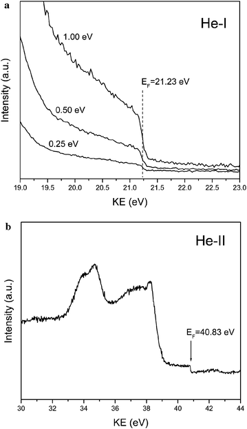 | ||
| Fig. 1 (a) He-I UPS spectra measured for three different pass energies and (b) He-II UPS spectrum of a Au film. Notice that the location of the Fermi edge is in excellent agreement with the expected values. | ||
Kelvin probe measurements (KP probe from McCallister Technical Services, WA) were made to determine the work functions of these materials, however, these measurements were performed in ambient conditions. The work function of the tip (stainless steel) used for the contact potential difference measurements was 4.4 eV. Photoluminescence measurements were performed using Renishaw inVia Raman microscope with a CCD detector. The Photoluminescence spectra were taken in the energy range of 1.5 eV to 3 eV at −185 °C.
Results and discussion
Fig. 2 shows the current voltage characteristics of SnO2nanowire and nanoparticle based DSSCs. The current density (JSC) of nanowire based cells is 5.0 mA/cm2 and the open circuit potential (VOC) is 518 mV. The JSC and VOC of the nanoparticle electrodes are 10.3 mA/cm2 and 332 mV, respectively. These values are similar to that presented in our previous study10 and are within the range of values obtained using about 30 samples or more. The higher JSC in the nanoparticle based cells can be explained from the high surface area of the nanoparticle electrode compared to the nanowire electrode. Although higher currents are seen in nanoparticle electrodes, it is observed that the currents are only ∼2 times higher than with nanowire electrodes. This is in contrast to about 5 times higher surface area of nanoparticle electrodes than the nanowire electrodes, as was seen in our previous study.10 The VOC measured with various nanowire based DSSCs were in the range of 520–560 mV compared to about 320–370 mV for nanoparticle based cells. The observed difference of about 200–250 mV in open circuit voltage is considerable and also reproducible with thinner (<100 nm diameter) nanowire based electrodes.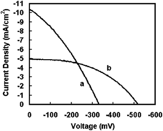 | ||
| Fig. 2 I-V characteristics of typical DSSCs made with SnO2 in our lab: (a) nanoparticles and (b) high aspect ratio branched nanowires. | ||
Transport and recombination characteristics
In order to understand the dynamics of electron transport in nanowires and nanoparticles, photocurrent decay measurements were performed using a range of photon fluxes. These measurements were performed on 8 µm thick films. The measurements showed that the electron transport time constant in nanowires was an order of magnitude faster than that of nanoparticle electrodes. The transport time constant showed a power law dependence with light intensity given by τc = A(Io)α−1, where A is a constant, Io is the incident light intensity and α is the disorder in the semiconducting film.14 The power law relation between the transport and light intensity is explained by random walk of electrons between the trap sites in the material, where the waiting time at each trap is in the form t−(1+α). The waiting times are modified when the states with the longest waiting times are filled, which leads to electron transport only through the unfilled states which are closer to the conduction band. A lower value of α implies a long tail of intraband gap distribution of states, and therefore higher disorder in the film either in terms of the density or distribution of electron traps in the film.15,16 The transport time constants obtained from these measurements are shown in Fig. 3. By fitting the transport time constants vs. light intensity, we obtain the value of α to be 0.35 and 0.8 for the nanoparticle and nanowire films, respectively. These values are different from what were observed in titania nanoparticles and nanotubes, where the α values were reported to be 0.4 and 0.14, respectively.14 The difference in these values suggests significant differences in the density and distribution of the transport limiting traps states in the two films. Further, the parameter α is related to the average trap depth of electrons in the material by the relation , where mc is the average trap depth below the conduction band in the semiconductor. From this relationship, it is estimated that mc for tin oxide nanowires and nanoparticles is 0.031 and 0.071 eV below the conduction band edge in nanowires and nanoparticles, respectively, implying the presence of higher density of trap states closer to the conduction band edge in the case of tin oxide nanowires.
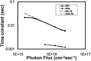 | ||
| Fig. 3 Transport time constants of nanowire- and nanoparticle-based DSSCs with light intensity. | ||
In order to determine the electron lifetimes in the nanoparticle and nanowire devices, open circuit photo voltage decay measurements were performed. The lifetimes obtained from these measurements are shown in the supplementary information taken from our previous study.10 This data is representative for all the electrodes used in this study. From these measurements, it is seen that the electron lifetimes are two orders of magnitude longer in nanowire electrodes than in nanoparticle electrodes. This difference definitely cannot be explained with the differences observed in the trap energy depths.
Although faster transport partly explains the decrease in the recombination in the nanowire based DSSCs, there may also be other reasons such as differences in the surfaces of the two materials, and their electronic properties which may result in different recombination times and VOC. Slower recombination may increase the electron density (nc) in the semiconductor films. The increase in the electron density in the illuminated state is related to the open circuit voltage by the expression17
 | (1) |
In this expression, kB is the Boltzmanns constant, T is the absolute temperature, nc and nco are the electron densities in the film in illuminated and dark states, Io is the light intensity, τ is the electron transport time constant, α is the disorder in the film14 and d is the thickness of the film. From equation (1), it is seen that higher electron density in the films results in higher open circuit potentials, which can explain the higher photovoltages seen in the nanowire electrodes. The electron lifetime in nanowires is two orders of magnitude longer than that in the nanoparticles, which can explain a difference of only 120 mV in the VOC values. This does not fully explain the ∼250 mV difference observed between nanowire and nanoparticle DSSCs. This implies that in addition to the differences in the electron transport and recombination characteristics within the SnO2nanowires and nanoparticles, the differences in their open circuit potentials could also be a result of the differences in their work functions. In order to understand these properties, UPS, Kelvin probe and photoluminescence spectroscopy techniques were used.
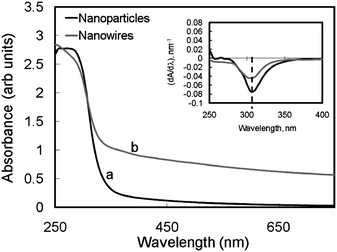 | ||
| Fig. 4 UV-Vis spectra of tin oxide nanowires and nanoparticles. | ||
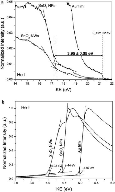 | ||
| Fig. 5 (a) High- and (b) low-KE slopes of the He-I UPS spectra obtained for Au film and SnO2nanoparticle and nanowire samples. | ||
The low resolution XPS spectra for both nanoparticle and nanowire samples were measured across the whole BE range, which show only peaks originating from Sn, O and Au, plus a weak C1s peak due to carbonaceous contamination. High resolution XPS spectra of Sn3d and O1s lines are compared in Fig. 7a and 7b, respectively. There is no substantial difference in the Sn3d spectra between the SnO2nanoparticle and nanowire samples. The BE of the Sn3d5/2 level measured for the nanowire sample (487.0 eV), as well as, the one measured for the nanoparticle sample (487.1 eV), agree very well with the value reported for SnO2.18 However, a clear difference is apparent for the O1s peak, where for the nanowire sample, there is an additional component at the high BE slope of the primary peak (Fig. 7b). In order to analyze this difference, the O1s peak was deconvoluted using the Gaussian function and the results are shown in Fig. 8. For the nanoparticle sample, a main peak at the BE of 531.1 eV and a second, minor peak at 532.5 eV were found (Fig. 8a). For the nanowire sample, the main peak is located at 530.9 eV and the 532.5 eV peak has much higher intensity than the one observed for the nanoparticles. In the nanowire sample, there is also a third, weak peak, at the BE of 533.9 eV.
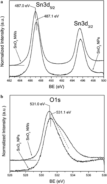 | ||
| Fig. 7 (a) Sn3d and (b) O1s XPS spectra measured for SnO2nanoparticle and nanowire samples. | ||
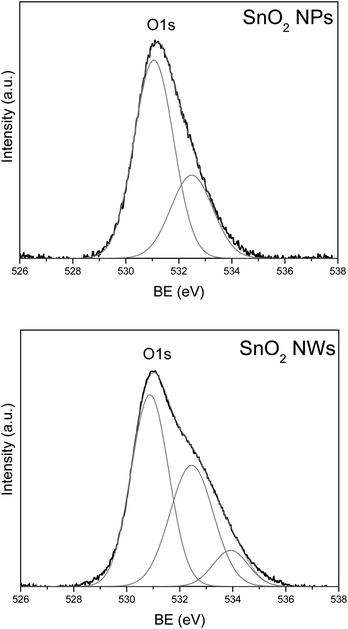 | ||
| Fig. 8 Deconvolution of the O1s XPS peak measured for the (a) nanoparticle and (b) nanowire sample. | ||
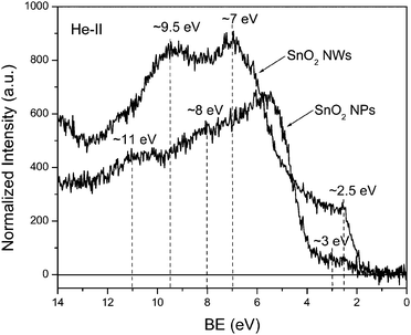
The asymmetry of the O1s peak, similar to that observed in our samples, has been reported recently for the SnO2nanowires and the peak at around 532.3 eV has been assigned to hydroxide and/or oxy-hydroxide.18 Also, the peak at 533.9 eV has been assigned to O1s line of molecular water.19 The XPS results suggest that the nanowire sample seems to have much higher concentration of hydroxide and/or oxy-hydroxide on the surface than the nanoparticle sample. This seems to explain the observed difference in the He-II UPS spectra. The spectrum measured for the nanoparticle sample is very similar to the spectrum of the typical SnO2 sample, with the peaks at 5.5, 8 and 11 eV originating from the O2p, Sn5p–O2p, and Sn5s–O2p states, respectively.20,21 On the other hand, the spectrum measured for the nanowire sample, contains strong peaks at ∼7 and ∼9.5 eV, which correlates with the locations of 1π and 3σ states of OH group.19,22
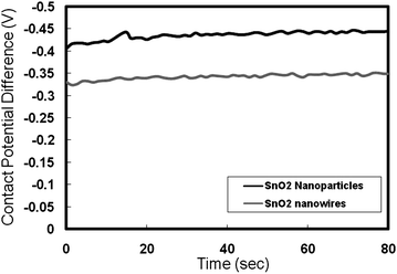 | ||
| Fig. 9 Contact potential differences with time for SnO2nanoparticle and nanowire sample. | ||
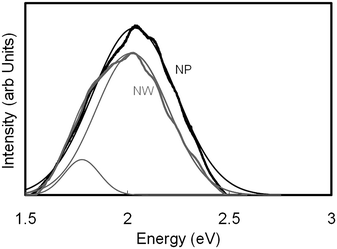 | ||
| Fig. 10 Photoluminescence spectra of SnO2nanowires and nanoparticles. | ||
(i) From the UV-Vis measurements, the bandgap of both nanowire and nanoparticle based materials is estimated to be approximately 4 eV.
(ii) From the contact potential difference measurements using the Kelvin probe, the work function of the nanowires and nanoparticles was estimated to be 4.75 and 4.85 eV, respectively. These values are consistent with the values reported in the literature for the work functions in aqueous media at pH = 1. However, in case of DSSC the electrolyte is in an organic form which has different pH value and thus a different work function. Typically, in TiO2 based DSSC, the work function of TiO2 is 3.95 eV (−0.45 V vs.NHE) with Fermi level around −0.45Vvs.NHE. The redox couple lies at −4.9 eV (−0.5 V vs.NHE). This gives the maximum voltage of 900–950 mV. Taking the value of the TiO2 conduction band as the reference, the conduction band of SnO2nanoparticles in organic electrolyte lies at about −4.4 eV from the fact that the conduction band edge of SnO2 lies ∼0.5 eV more positive than that of TiO2.2 The value for the SnO2nanowires is 4.3 eV corresponding to the differences seen from Kelvin probe measurements. From these measurements, the maximum attainable VOC in the SnO2nanoparticles is 500 mV and in nanowires is 600 mV.
(iii) From the UPS measurements, the work function of SnO2nanoparticles and nanowires was determined to be 4.4 and 4.0 eV, respectively. This difference is more than what was measured using the Kelvin probe technique. The higher difference in the work functions is most likely due to the desorption of the adsorbed species from the surfaces in the UHV conditions, exposing the pure nanowire and nanoparticle surfaces during the UPS measurements. Additionally, the XPS analysis indicated a strong presence of hydroxide and/or oxy-hydroxide on the nanowire samples, where as in the case of SnO2nanoparticles, such species were absent. During the Kelvin probe measurements however, these differences are suppressed due the presence of adsorbed water on the surfaces of both, the nanoparticles and nanowires.
(iv) From photoluminescence measurements, assuming the transitions occur from the conduction band edge to the mid bandgap states, additional luminescence peak was observed at 1.75 eV for nanowires, implying the presence of external states. Both, the nanowires and the nanoparticles, however had peaks at 2 eV.
(v) The average trap depth, mc, was 0.03 eV below the conduction band edge for nanowires while the mc for the nanoparticles was estimated to be about 0.07 eV below the conduction band edge. This implies that for same photoelectron density, nanowires will show a higher VOC than the nanoparticles.14
From the above measurements it can be seen that the nanowires have additional states above the states available in nanoparticles and also have a shallow trap state distribution than in the nanoparticle electrodes. Electron trapping and detrapping is faster in shallow trap states, which can explain the fast electron transport observed in nanowire electrodes. The high VOC of the nanowire electrodes is, however related to both, the shallow trap states and surface of the nanowires. UPS and Kelvin probe measurements indicate that the work functions of nanowires are smaller than that of nanoparticles. Using this information, a model can be put together which shows roughly the electronic structure within the nanowire and nanoparticles. Fig. 11a shows the schematic representation of the energy levels determined from UPS and Kelvin probe measurements. The energy levels in the DSSCs made with nanoparticle and nanowire electrodes are shown in Fig. 11b. It is possible that dye–tin oxide interactions are different for nanoparticles and nanowires. But, the nanoparticle electrodes in this study have consistently shown high current densities (∼10 mA/cm2), indicating that the observed lower open circuit voltage cannot be attributed to poor dye interaction with the surface. Further studies to understand dye uptake, interfacial chemistry and electron injection processes will be crucial to improve the stability and current density of tin oxide nanowire based DSSCs. In addition to DSSCs, because of potentially better transport properties, SnO2nanowires are finding increased applications in photoelectrochemical cells,23 and Li-ion batteries.24
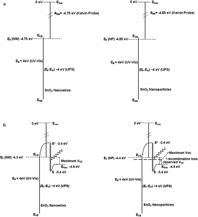 | ||
| Fig. 11 (a) The electronic structure of the SnO2nanoparticles and nanowires expected in acidic aqueous medium based on Kelvin probe measurements. (b) Energy level diagram in SnO2 expected with nanowires and nanoparticles in organic electrolyte medium. The apparent shifts in the band edges are adjusted based on known band edge position of SnO2 in organic electrolyte. | ||
Summary
In the above study the origin of higher VOC in SnO2nanowires based DSSCs compared to nanoparticle based DSSCs was investigated. Studies showed that the higher VOC in nanowire based DSSCs is a result of both, a difference in the density and distribution of trap states in these two materials and also due to a difference in the work functions of SnO2nanowires and nanoparticles.Acknowledgements
The authors gratefully acknowledge the financial support from the U.S. Department of Energy (DE-FG02-05ER64071 and DE-FG02-07ER46375). Authors also appreciate the Institute for Advanced Materials and Renewable Energy (IAM-RE) at University of Louisville for access to various techniques used for the studies.References
- N. G. Park, M. G. Kang, K. S. Ryu, K. M. Kim and S. H. Chang, J. Photochem. Photobiol., A, 2004, 161, 105 CrossRef.
- I. Bedja, S. Hotchandani and P. V. Kamat, J. Phys. Chem., 1994, 98, 4133 CrossRef CAS.
- A. Kay and M. Gratzel, Chem. Mater., 2002, 14, 2930 CrossRef CAS.
- S. Chappel and A. Zaban, Sol. Energy Mater. Sol. Cells, 2002, 71, 141 CrossRef CAS.
- K. Sayama, H. Sugihara and H. Arakawa, Chem. Mater., 1998, 10, 3825 CrossRef CAS.
- J. Bandara and K. Tennakone, J. Colloid Interface Sci., 2001, 236, 375 CrossRef CAS.
- Y. Fukai, Y. Kondo, S. Mori and E. Suzuki, Electrochem. Commun., 2007, 9, 1439 CrossRef CAS.
- N. N. Dinh, M.-C. Bernard, A. H.-L. Goff, T. Stergiopoulos and P. Falaras, C. R. Chim., 2006, 9, 676 CrossRef CAS.
- A. J. Nozik and R. Memming, J. Phys. Chem., 1996, 100, 13061 CrossRef CAS.
- S. Gubbala, V. Chakrapani, V. Kumar and M. K. Sunkara, Adv. Funct. Mater., 2008, 18, 1.
- N. Kopidakis, K. D. Benkstein, J. van de Lagemaat and A. J. Frank, J. Phys. Chem. B, 2003, 107, 11307 CrossRef CAS.
- E. Galoppini, J. Rochford, H. Chen, G. Saraf, Y. Lu, A. Hagfeldt and G. Boschloo, J. Phys. Chem. B, 2006, 110(33), 16159 CrossRef CAS.
- A. Zaban, M. Greenshtein and J. Bisquert, ChemPhysChem, 2003, 4, 859 CrossRef CAS.
- K. Zhu, N. R. Neale, A. Miedaner and A. J. Frank, Nano Lett., 2007, 7, 69 CrossRef CAS.
- J. Nelson, S. A. Haque, D. R. Klug and J. R. Durrant, Phys. Rev. B: Condens. Matter Mater. Phys., 2001, 63, 205312 CrossRef.
- J. Nelson, Phys. Rev. B: Condens. Matter Mater. Phys., 1999, 59, 15374 CrossRef CAS.
- L. M. Peter, Phys. Chem. Chem. Phys., 2007, 9, 2630 RSC.
- A. Kar, J. Y. Yang, M. Dutta, M. A. Stroscio, J. Kumari and M. Meyyappan, Nanotechnology, 2009, 20(6), 65704 CrossRef.
- P. A. Thiel and T. E. Madey, Surf. Sci. Rep., 1987, 7, 211 CrossRef CAS.
- J. M. Themlin, R. Sporken, J. Darville, R. Caudano, J. M. Gilles and R. L. Johnson, Phys. Rev. B: Condens. Matter Mater. Phys., 1990, 42, 11914 CrossRef CAS.
- M. Sinner-Hettenbach, N. Barsan, U. Weimar, T. Weiss, H. von Schenck, M. Gothelid, L. Giovanelli and G. Le Lay, Thin Solid Films, 2001, 391, 192 CrossRef CAS.
- K. F. Zheng, Y. H. Yu, Q. L. Guo, S. Liu, E. G. Wang, F. Xu and P. J. Moller, J. Phys.: Condens. Matter, 2005, 17, 3073 CrossRef CAS.
- C. Santato, C. Lopez and K. S. Choi, Electrochem. Commun., 2007, 9, 1519 CrossRef CAS.
- P. Meduri, C. Pendyala, V. Kumar, G. U. Sumanasekera and M. K. Sunkara, Nano Lett., 2009, 9, 612 CrossRef CAS.
Footnote |
| † Electronic supplementary information (ESI) available: The electron lifetime of SnO2 nanowires and nanoparticles. See DOI: 10.1039/b910174h |
| This journal is © The Royal Society of Chemistry 2009 |

