Germanium-catalyzed hierarchical Al2O3 and SiO2nanowire bunch arrays
Zhanjun
Gu
ab,
Feng
Liu
ab,
Jane Y.
Howe
c,
M.
Parans Paranthaman
d and
Zhengwei
Pan
*ab
aFaculty of Engineering, University of Georgia, Athens, GA 30602, USA. E-mail: panz@uga.edu; Fax: +1-706-542-8806; Tel: +1-706-542-4657
bDepartment of Physics and Astronomy, University of Georgia, Athens, GA 30602, USA
cMaterials Sciences and Technology Division, Oak Ridge National Laboratory, Oak Ridge, Tennessee 37831, USA
dChemicals Sciences Division, Oak Ridge National Laboratory, Oak Ridge, Tennessee, 37831, USA
First published on 23rd September 2009
Abstract
Germanium (Ge), a Group IV semiconductor, was recently used as an effective catalyst to grow individual, single-crystalline ZnOnanowires through a vapor-liquid-solid (VLS) process [Pan et al., Angew. Chem., Int. Ed., 2005, 44, 274–278]. Here, we show that Ge can also act as an efficient catalyst for the large-scale growth of highly aligned, closely-packed polycrystalline Al2O3 and amorphous SiO2nanowire bunch arrays. The Ge-catalyzed Al2O3 and SiO2nanowire growth exhibits many interesting growth behaviors including (i) multiple nanowire growth catalyzed by one micrometer-size Ge particle, (ii) branching growth and (iii) batch-by-batch growth. These growth phenomena are distinct from the conventional Au-catalyzed nanowire growth but are analogous to the recently reported Ga-catalyzed SiO2nanowire growth. It is anticipated that many other oxidenanowires and nanowire assemblies can be synthesized through the Ge-catalyzed VLS process. The Ge-catalyzed Al2O3 and SiO2nanowires emit strong visible light under ultraviolet light excitation.
Introduction
The vapor-liquid-solid (VLS) whisker growth mechanism, proposed by Wagner and Ellis in 1964 for silicon whisker growth,1 is the fundamental mechanism for the growth of one-dimensional nanomaterials. So far, this mechanism has been successfully employed to fabricate carbon nanotubes2,3 and a wide range of nanowires, including Group IV (e.g., Si and Ge),4–6 III–V (e.g., GaAs and GaP),7–9 and II–VI (e.g., ZnS and ZnSe) semiconductors,7,10oxides (e.g.ZnO),11,12nitrides (e.g., GaN),13,14etc. In this mechanism, a catalystnanoparticle serves as a preferential site for the absorption and dissolution of reactants from the vapor phase, directs the nanowire's growth direction, and defines the nanowire's diameter. A common morphological feature of VLS-grown nanowires is that each nanowire is terminated at its growth front by a catalystnanoparticle with a diameter comparable to that of the connected nanowire.For nanowire growth, the most commonly used catalysts are gold (Au) and iron (Fe). In particular, Au can almost act as a universal catalyst for many semiconductor and oxidenanowires.4–14 Recently, several new catalysts, which mainly function for some specific oxides, were discovered. These mainly include gallium (Ga), a low-melting point metal, for SiO2nanowire growth15–20 and germanium (Ge), a Group IV semiconductor, for ZnOnanowire growth.21 Compared with Au and Fe, these new catalysts exhibit many novel, interesting nanowire growth phenomena and result in the formation of complex, self-assembled nanowire superstructures, which were not observed in Au- (or Fe-) catalyzed conventional VLS growth processes. In Ga-catalyzed SiO2nanowire growth, for example, a micrometer-sized Ga droplet can simultaneously catalyze the growth of hundreds of thousands of aligned SiO2nanowires, forming closely packed nanowire assemblies with various complex morphologies.15–17 In Ge-catalyzed ZnOnanowire growth, on the other hand, the nanowire growth rate is about one order of magnitude faster than Au-catalyzed ZnOnanowires and the diameter of the nanowires is less dependent on the Ge particle size.21 It is apparent that the new catalysts not only facilitate the fabrication of high quality oxidenanowires and nanowire assemblies, but also enrich our understanding of the current VLS growth mechanism and thus expand the VLS mechanism to a broader range.
In this article, we further extend the VLS mechanism by using Ge as a catalyst to grow hierarchical Al2O3 and SiO2nanowire bunch arrays. The phenomena observed in Ge-catalyzed Al2O3 and SiO2nanowire growth are similar to those which occur in Ga-catalyzed SiO2nanowire growth,15–17 suggesting Ge and Ga share similar catalytic effects and mechanisms. A comparison of the present growth with the previously reported VLS nanowire growth phenomena is given consistently throughout the article. The efficient catalytic effects of Ge on the growth of Al2O3, SiO2 and ZnO21nanowires suggest that many other oxidenanowires may be synthesized through the Ge-catalyzed VLS process.
Experimental
Materials and substrate
Aluminium (Al) particulates with size of ∼10–20 µm and Al foils with thickness of ∼0.5 mm were used as the Al sources. Ge powder was used as the Ge source. Alumina plates and Si wafers were used as the supporting and/or growth substrates. Ultrahigh-purity (UHP) oxygen gas was used as the oxygen source and UHP argon was used as the carrier gas.Growth of nanowires
The nanowire growth was conducted in a tube furnace system similar to that described in ref. 15. In a typical run, about 0.2 g Ge powder was placed at the center of an alumina tube that was inserted in a horizontal tube furnace. For the growth using Al particulates as the Al source, Al particulates were spread on an alumina substrate which was located at about 5 cm downstream of the Ge powder. For the growth using Al foil as the Al source, a piece of 5 mm × 5 mm Al foil was placed on a Si wafer strip (5 cm long and 3 cm wide). After evacuating the alumina tube to ∼2 × 10⁻³ Torr, 100 sccm (standard cubic centimeter per minute) flowing argon was introduced into the reaction chamber and the furnace was quickly heated to 1000 °C. About 1–5 sccm oxygen was then added through a long, thin alumina tube to a position right above the growth zone. The introduction of oxygen behind the Ge source can avoid the pre-oxidization of Ge powder, while generating an efficient, wide oxidizing region over the growth zone to facilitate the oxidenanowire growth. At 1000 °C, the Ge vapor generated from the Ge powder was transported by the argon carrier gas to the growth zone, where the temperature is in the range of 700 to 850 °C, to feed the nanowire growth. The pressure of the reaction chamber was held at 300 Torr and the growth time varied from 10 to 30 minutes. The furnace was then cooled naturally to room temperature in a flowing Ar atmosphere.Characterization
The as-synthesized products were characterized and analyzed by X-ray diffractometry (XRD; PANalytical X'Pert PRO diffractometer with Cu Kα radiation), scanning electron microscopy (SEM; FEI Inspec F FEG SEM at 15 kV), transmission electron microscopy (TEM; Hitachi HF-3300 FEG TEM/STEM at 300 kV), and energy-dispersive X-ray spectroscopy (EDS) attached to the SEM and TEM. The photoluminescence (PL) properties were studied with a Horiba Jobin Yvon FluoroLog3-2iHR320 spectrofluorometer using a Xe lamp as the excitation source. For SEM investigation, the products together with the growth substrate were directly transferred into the SEM chamber without destroying the location and orientation of the products on the substrates. For TEM studies, the products were gently scraped off the substrate using sharp tweezers and were directly mounted on a Cu folding TEM grid without carbon supporting film. Such a sample preparation method can help to maintain the shape of the nanowire assemblies and the positional relationship between the catalyst particles and the nanowires.Results and discussion
Here, we report the results obtained for two scenarios: Al particulates on alumina plates and Al foils on Si wafer.A. Aluminium particulates on alumina substrates
After the growth, each Al particulate was covered with a thick layer of white-colored, wool-like product. XRD analyses (Fig. 1) reveal the presence of Al2O3 (JCPDS card No. 5-712), Ge (JCPDS card No. 4-545), and Al (JCPDS card No. 65-2869) crystalline phases in the products. The Al peaks are believed to come from the unreacted Al particulates. The strong peaks from Ge indicate the presence of a significant amount of crystalline Ge in the products. No peaks related to GeO2 were detected, indicating that oxygen preferentially reacts with Al to form stable Al2O3.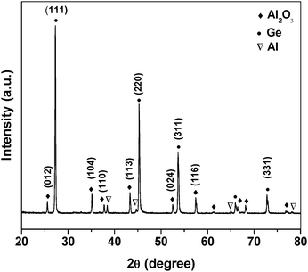 | ||
| Fig. 1 XRD pattern of Ge-catalyzed Al2O3nanowires. | ||
Fig. 2a shows a low-magnification SEM image of the Ge-Al2O3 products formed on one Al particulate. Dark particles with diameters of 1–5 µm are distributed on the top of a dense, aligned microrod layer. High-magnification SEM observations (Fig. 2b–g) reveal that each microrod is actually composed of a micrometer-sized particle and a bunch of highly aligned, closely packed nanowires. EDS analyses (Fig. 3) show that the particles are Ge with a small amount of Al and O (Fig. 3b), whereas the nanowires contain Al and O with traces of Ge (∼1 atom%) (Fig. 3c). The EDS results, together with the XRD results (Fig. 1), indicate that the particles on top of the nanowire bunches are crystalline Ge and that the nanowires are Ge-doped crystalline Al2O3. The presence of a Ge particle on the top of an Al2O3nanowire bunch suggests that the Al2O3nanowires were grown through a Ge-catalyzed VLS process and that one micrometer-sized Ge particle can simultaneously catalyze the growth of numerous Al2O3nanowires.
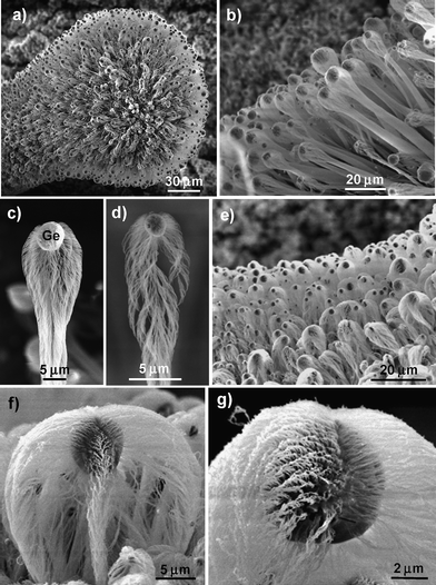 | ||
| Fig. 2 SEM images of Ge-catalyzed Al2O3nanowire bunches. (a) Low-magnification SEM image of dense Al2O3nanowire bunches grown around an Al particulate. (b) Aligned baseball bat-like Al2O3nanowire bunches. (c) One dense-packed baseball bat-like Al2O3nanowire bunch. (d) One loose-packed baseball bat-like Al2O3nanowire bunch. (e) Aligned spindle-like Al2O3nanowire bunches. (f,g) Individual spindle-like Al2O3nanowire bunches. | ||
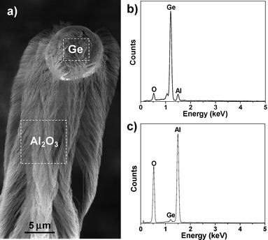 | ||
| Fig. 3 EDS analyses on Ge-catalyzed Al2O3nanowire bunch. (a) SEM image of a Ge-catalyzed Al2O3nanowire bunch. The dash-line squares represent the positions where the EDS spectra were taken. (b) EDS spectrum taken from the Ge catalyst particle. (c) EDS spectrum taken from the Al2O3nanowire bunch. | ||
Based on the morphologies, two types of nanowire bunches can be distinguished: baseball bat-like bunches (Fig. 2b–d) formed at ∼700–800 °C and spindle-like bunches (Fig. 2e–f) grown at ∼800–850 °C. The baseball bat-like bunches are thin and long (the length can be up to 500 µm) and the nanowires are grown mainly from the Ge particle's lower hemisphere surface (Fig. 2c,d). In contrast, the spindle-like bunches are thick (the diameters can be up to 20 µm) and short and the entire surface of the Ge particle is covered with dense Al2O3nanowires (Fig. 2f,g). No matter what the shape of the nanowire bunches, the bunches always tend to grow along the Al particulate's surface normal to form quasi-aligned bunch arrays (Fig. 2b,e). The nanowires inside each bunch, on the other hand, tend to pack conically around the bunch's central axis (refer to the TEM images in Fig. 4), therefore forming complex, hierarchical Al2O3nanowire superstructures.
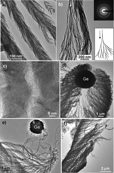 | ||
| Fig. 4 TEM images of Ge-catalyzed Al2O3nanowire bunches. (a) Low-magnification TEM image of the stem part of three parallel baseball bat-like nanowire bunches. The inset demonstrates how the nanowires pack into nanowire bunches. (b) A high-magnification TEM image of a bunch of Al2O3nanowires showing branching-growth features. Bottom right inset, schematic diagram of the branching-growth model. Top right inset, electron diffraction pattern of the polycrystalline Al2O3nanowires. (c) High-resolution TEM image of two Al2O3nanowires. (d,e) Top part of spindle-like Al2O3nanowire bunches. (f) A broken Al2O3nanowire bunch. The white dot-dash line represents the central axis of the bunch. The white dash lines represent the orientation of nanowires in the bunch. | ||
The morphological features of the nanowire bunches and the relationship between the Ge particles and Al2O3nanowires can be better displayed by TEM imaging. Fig. 4a shows a low-magnification TEM image of the stem part of three parallel baseball bat-like nanowire bunches. The nanowire bunches resemble the structure of a straw rope. Due to the short lengths of the nanowires (from several hundreds of nanometers to several micrometers), the bunch is not made of continuous nanowires that go through the entire length of the bunch; instead, it is piled up by nanowires that are conically arranged at an angle of 10–40° around the bunch's central axis (see the schematic drawing inserted in Fig. 4a). High-magnification TEM imaging (Fig. 4b) shows that branching growth15 occurs in the Al2O3nanowire growth process; that is, one nanowire splits into two branches, and the newly formed branch also splits into two sub-branches, and so on (see model inserted in Fig. 4b). It is this branching growth that makes the nanowires connect together and form a long, continuous nanowire bunch. Electron diffraction patterns recorded from the nanowire bunches display sharp diffraction rings (inset in Fig. 4b), indicating that the Al2O3nanowires are polycrystalline. The polycrystalline nature of the Al2O3nanowires is further confirmed by high-resolution TEM imaging, as shown in Fig. 4c, where a chain of elongated Al2O3nanoparticles with different lattice orientation can be clearly seen. The Al2O3nanowires are very thin with diameters in the range of 10 to 20 nm.
Fig. 4d–f show the TEM images of the spindle-like Al2O3nanowire assemblies. In Fig. 4d, the position of a Ge particle at the top of a nanowire bunch is well preserved. It clearly shows that numerous Al2O3nanowires are grown from a 4 µm diameter Ge particle and that the bunch is piled up by numerous conically arranged nanowires. The amount and volume of the nanowires increase quickly with the increase of the distance from the Ge particle, which is a result of the branching growth. The branching growth phenomenon is further demonstrated by Fig. 4e, in which the amount and volume of the nanowires increase tens of times within a short distance (∼5 µm). Fig. 4f shows half of a spindle-like nanowire bunch (it can be considered as the left half of the spindle in Fig. 4d), clearly showing both the branching growth phenomenon and the conical arrangement of nanowires around the bunch's central axis.
The TEM images in Fig. 4 and the SEM images in Fig. 2 show that most of the nanowires in a bunch have already detached from the Ge catalyst particles. This phenomenon suggests that the Ge-catalyzed Al2O3 bunches are formed by a batch-by-batch growth manner, which is similar to the Ga-catalyzed SiO2nanowire bunch growth.15,16 That is, for each batch, many Al2O3nanowires simultaneously nucleate on the Ge particle's surface, grow at nearly the same rate, and simultaneously detach from the Ge particle because of the force exerted by the newly formed batch above (refer to the growth model proposed in ref. 15). As a result of the batch-by-batch growth, the Ge particle is pushed away from the aluminium particulate surface, lifted upward by the growing nanowire batches, and finally located at the top of the nanowire bunch (see the images in Fig. 2). From this point of view, the nanowire bunch is composed of many batches of nanowires that are ricked one by one along the bunch's growth direction, which is clearly displayed by Fig. 2c, d, 3a, 4a, d and f.
B. Aluminium foils on silicon wafer
We also placed a small piece of aluminium foil (5 mm × 5 mm) on a Si wafer surface to repeat the growth obtained on Al particulates. Surprisingly, not only Al2O3nanowire bunch arrays were grown on Al foil and a nearby circular region on the Si wafer, but aligned SiO2nanowire assemblies were also obtained in an outer circular region on the Si wafer. Based on the composition and morphology of the products, three concentric band regions around the Al foil can be identified, as shown schematically in Fig. 5. The diameters of regions A, B and C are about 10 mm, 18 mm and 25 mm, respectively.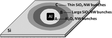 | ||
| Fig. 5 Schematic diagram of the growth regions of Ge-catalyzed Al2O3nanowires (NW) and SiO2nanowires formed on a Si substrate. Around the Al foil (5 mm by 5 mm), three concentric band regions were identified based on the composition and morphology of the products. The products in Region A (diameter: ∼10 mm), Region B (diameter: ∼18 mm) and Region C (diameter: ∼25 mm) are Al2O3nanowire bunches, spindle-like SiO2nanowire bunches and small SiO2nanowire bunches, respectively. | ||
In region A (including the Al foil), the morphology, composition and microstructures of the products are similar to the Ge-Al2O3nanowire bunches grown on Al particulate surfaces as shown in Fig. 2–4, except that a small amount of Si was detected in the Al2O3nanowire bunches. In region B, dense, highly aligned, spindle-like nanowire bunch arrays were grown on the Si wafer surface (Fig. 6a,b). Even though the morphology of these spindles is similar to the nanowire bunches formed in region A and the top particles of the spindles are also Ge (with small amounts of O and Si, Fig. 6c), EDS analysis (Fig. 6d) shows that the dominant components of the nanowire bunches are Si and O, with Ge and Al as the minor components. This indicates that the nanowires grown in region B are SiO2 doped with Ge and Al. The SEM and EDS results clearly show that Ge can act as an efficient catalyst for the growth of not only Al2O3nanowires but also SiO2nanowires.
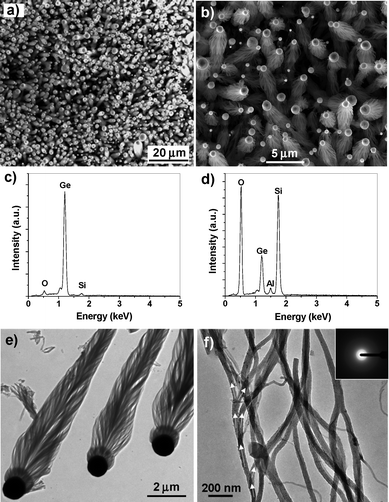 | ||
| Fig. 6 Electron microscope images and EDS spectra of Ge-catalyzed SiO2nanowire bunches grown in region B in Fig. 5. (a) Low-magnification and (b) high-magnification SEM images of dense spindle-like SiO2nanowire bunches. (c) EDS spectrum taken on Ge catalyst particle. (d) EDS spectrum recorded from SiO2nanowire bunch. (e) Low-magnification TEM image of three Ge-catalyzed SiO2nanowire bunches. (f) High-magnification TEM image of SiO2nanowires. The white arrow heads show the branching-growth trail. Inset, electron diffraction pattern of the amorphous SiO2nanowires. | ||
Fig. 6e is a low-magnification TEM image of three well-preserved Ge-SiO2nanowire spindles. The morphology of the Ge-SiO2 spindles is exactly the same as the Ga-SiO2 spindles reported previously.16 The diameter of the Ge particles is about 1 µm and the length of the nanowire bunches is up to 10 µm. Fig. 6e also clearly shows that the nanowire bunches are piled up by numerous conically arranged nanowires around the bunch's central axis. The lengths of the nanowires are in the range of 1–3 µm. Fig. 6f is a high-magnification TEM image of the SiO2nanowires. These nanowires have a very uniform diameter of ∼40 nm. Branching growth occurs in SiO2nanowire growth, as indicated by the white arrow heads in Fig. 6f. Electron diffraction analysis shows that the SiO2nanowires are amorphous (inset in Fig. 6f).
The nanowires grown in region C are also SiO2, but the sizes of the nanowire bunches and the associated Ge particles (Fig. 7) are much smaller than the structures formed in region B (Fig. 6). As discussed below, this is mainly because the concentration of Si reactant species in region C is lower than that in region B.
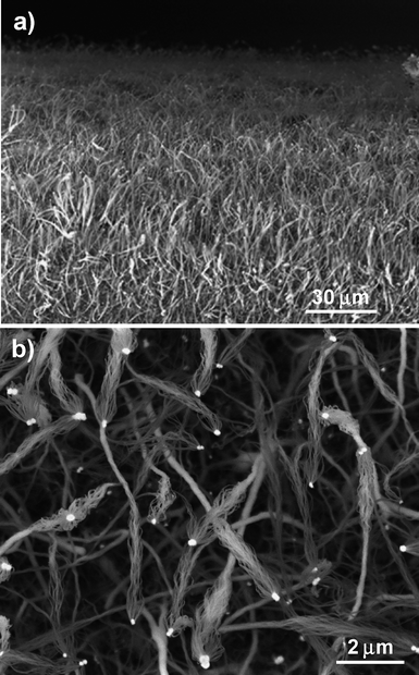 | ||
| Fig. 7 (a) Low-magnification and (b) high-magnification SEM images of Ge-catalyzed SiO2nanowire bunches grown in region C in Fig. 5. | ||
The above results suggest that Si was utilized in the nanowires growth. The Si reactant was provided through the etching of the Si wafer by the molten Al (melting temperature, 660.4 °C) at temperatures of 700–850 °C. Indeed, we note that after the growth, the edge of the Al foil melts with the Si wafer to form an Al-Si alloy band around the Al foil. The width of the Al-Si band is about 3 mm. The melting of the Al foil and the etching of the Si wafer generate a dense vapor of Si species and Al species around the Al foil area, which act as Si and Al sources for the growth of SiO2 and Al2O3nanowires, respectively. In region A, the Al species is dominant, leading to the formation of Si-doped Al2O3nanowires. In region B, on the other hand, the Si species is the dominant reactant, which facilitates the growth of Al-doped SiO2nanowires. In region C, the Si species concentration is much lower than that in region B due to its greater distance from the Al-Si melting zone, resulting in the formation of thinner and less-dense SiO2nanowire bunches.
C. Growth mechanism
The above results indicate that semiconductor Ge can serve as an effective catalyst for the growth of polycrystalline Al2O3nanowire assemblies and amorphous SiO2nanowire bunches via a VLS process. This is the first example of using Ge as a catalyst to grow Al2O3nanowires (Al2O3nanowires were mainly prepared by chemical etching or anodization of Al),22–28 as well as SiO2nanowires. The phenomena observed in Ge-catalyzed Al2O3 and SiO2nanowire growth are distinct from the conventional Au-catalyzed nanowire growth4–14 and the newly reported Ge-catalyzed ZnOnanowire growth,21 where one catalyst particle can only catalyze the growth of one nanowire. Our Ge-catalyzed Al2O3 and SiO2nanowire growth, however, is analogous to the Ga-catalyzed SiO2nanowire growth15–17 in many aspects including (1) multiple nanowires growth by one micrometer-sized catalyst particle, (2) branching growth, and (3) batch-by-batch growth. These similarities suggest that the growth mechanism and growth model proposed for Ga-catalyzed SiO2nanowire assemblies in ref. 15 is suitable to account for the Ge-catalyzed Al2O3 and SiO2nanowire assemblies described here.For a better understanding of the Ge-catalyzed Al2O3 and SiO2nanowire growth, besides the branching growth and batch growth phenomena described in previous sections, the following four aspects are addressed.
(1) For a VLS process to occur, a eutectic alloy between the catalyst and nanowire materials needs to be formed.1,5,7 Although no Ge-Al2O3 and Ge-SiO2 ternary phase diagrams are available, the Ge-Al, Ge-Si, and Si-Al binary phase diagrams29 suggest that eutectic alloys of Ge-Al (for Al2O3nanowires) and Ge-Si-Al (for Al-doped SiO2nanowires) can be formed at growth temperatures of 700–850 °C. This implies that a Ge-catalyzed VLS-type process can take place. When the eutectic alloy droplets become supersaturated in Al (or Si), numerous Al2O3 (or SiO2) nuclei will precipitate on the Ge particle surface (especially on the Ge particle's lower hemisphere surface) and grow into nanowires, possibly by the in-situ reaction between Al (or Si) and O, as happens in Ge-catalyzed ZnOnanowire growth.21
(2) Even though the Al2O3 and SiO2nanowire bunches are grown from Al particulates (or Al foil) and Si wafer, respectively, the fact that the Ge catalyst particles always appear at the top of the nanowire bunches (Fig. 2, 6 and 7) suggests that the reactants (Ge, Al, or Si) are fed from the vapor. The Ge and Al vapors are provided by thermal evaporation of Ge and Al powders, respectively, whilst the Si vapor is generated by molten Al etching of Si wafer. Since the feeding of Ge vapor continues during the whole growth process, the sizes of the Ge particles increase with reaction time by continuously absorbing Ge species from the vapor, resulting in the nucleation and growth of many more nanowires. This is the reason why the diameter of the nanowire bunch increases from the bottom to the top (Fig. 2c, d, f, 6b and e).
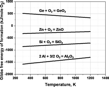
(3) From the thermodynamic point of view, in order to grow Al2O3 and SiO2nanowires using Ge as the catalyst in the presence of a certain amount of oxygen, the Gibbs free energies of formation for GeO2, Al2O3 and SiO2 should be compared. Fig. 8 shows plots of the standard Gibbs free energies of oxidation of selected metals taken from the standard Gibbs energies of reaction tables.30 From Fig. 8, it can be clearly seen that, by using Ge as the catalyzing agent, one can selectively oxidize Al or Si over Ge. This is true for Ge-catalyzed ZnOnanowire growth21 also where ZnO is more stable under the process conditions.
(4) During experiments we found that oxygen plays a critical role in Al2O3 and SiO2nanowire growth and a very small change in oxygen content can cause large changes to the yield and quality of the products. The optimum oxygen flow rate for high-yield growth of Al2O3 and SiO2nanowire assemblies is 2–3 sccm. If the oxygen flow rate is around 1 sccm, the yield of nanowires is very low due to the lack of enough oxygen to oxidize Al and Si precipitated from the Ge catalyst particles. When the oxygen flow rate is 3–4 sccm, pure nanowire assemblies without Ge catalyst particles at the top can be obtained, like the SiO2nanowire assemblies shown in Fig. 9. This is because the Ge particles were oxidized into volatile GeO. This oxidization process may happen at the later growth stage since well-preserved hemispherical hollows can be clearly seen at the top of the nanowire assemblies (Fig. 9a), which are apparently left by the Ge catalyst particles. Sometimes, a small Ge particle that is yet to be evaporated remains inside the hollow hemisphere (Fig. 9b). If the oxygen flow rate is larger than 4 sccm, rather than Al2O3 and/or SiO2nanowire assemblies, a large amount of single-crystalline GeO2nanowire networks are formed (results not shown here). This is probably because at higher oxygen concentration, the Al source is totally oxidized and thus fails to provide Al reactant vapor to feed the nanowire growth.
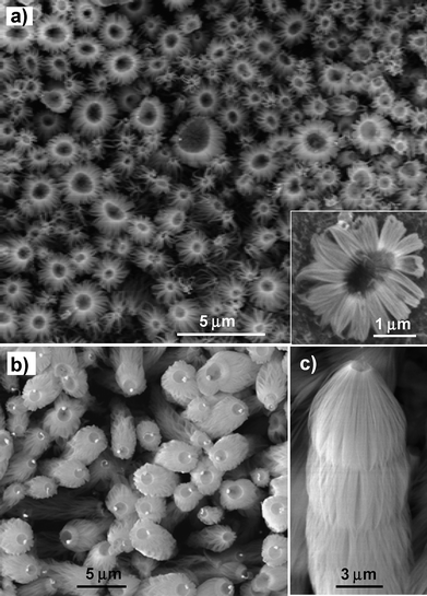 | ||
| Fig. 9 SEM images of Ge-catalyzed SiO2nanowire bunches grown under high oxygen concentration. (a) Low-magnification SEM image showing SiO2nanowire bunches with Ge particles being evaporated. Inset, high-magnification image of SiO2nanowire bunch. (b) SiO2nanowire bunches with small yet evaporated Ge particles on the top. (c) A pure SiO2nanowire bunch. | ||
D. Photoluminescence properties
Under 254 nm UV lamp irradiation, bright blue and blue-white emissions are visible for the Ge-catalyzed Al2O3 and SiO2nanowires, respectively, even under room light condition. Fig. 10a shows a room-temperature PL spectrum recorded from Al2O3nanowires grown on Al particulates under 300 nm UV light excitation. A strong, broad blue emission band centered at ∼477 nm is detected. The blue emission from Al2O3 is usually attributed to the electronic transitions at the energy levels of F+ centers, which are oxygen vacancies with one electron.27,28 In our Ge-doped Al2O3nanowires, the substitution of Al3+ ions with Ge4+ ions increases the oxygen vacancies (F+ centers) in the Al2O3nanowires, which may be responsible for the bright blue emission.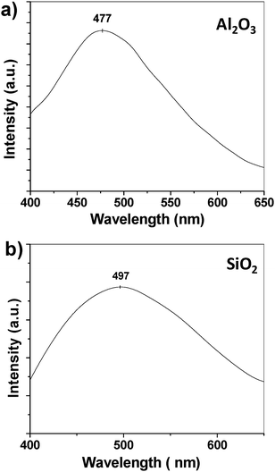 | ||
| Fig. 10 Photoluminescence (PL) spectra. (a) PL spectrum of Al2O3nanowires. The excitation wavelength is 300 nm. (b) PL spectrum of SiO2nanowires. The excitation wavelength is 254 nm. | ||
Fig. 10b is a room-temperature PL spectrum recorded from SiO2nanowires grown on Si wafer under 254 nm UV light excitation. A very broad emission band that covers almost the entire visible spectrum (from 400 nm to 650 nm) is obtained. The peak is centered at ∼497 nm. Due to the contribution from the yellow and red components, the light emitted from the SiO2nanowires under UV excitation appears to be white. In contrast, green-light emission is generally observed in previously reported bulk silica,31,32 and SiO2nanowires,18,33 and the origins of the green emission are controversial. Even though the origin of the blue-white light emission of the Ge-catalyzed SiO2nanowires is not clearly understood at the present stage, the Al2O3 and GeO2 components present in the SiO2nanowires (see Fig. 6d) should contribute to the broad band emission. The detailed fluorescence mechanism is under investigation.
Conclusions
Semiconductor Ge can act as an efficient catalyst for the high-yield growth of polycrystalline Al2O3nanowire bunches and amorphous SiO2nanowire bunches by a VLS process. The Ge-catalyzed Al2O3 and SiO2nanowire growth features (i) multiple nanowire growth catalyzed by one micrometer-size Ge particle, (ii) branching growth and (iii) batch-by-batch growth, which are different from the conventional Au-catalyzed nanowire growth but are analogous to the newly reported Ga-catalyzed SiO2nanowire growth. The present results, together with the recently reported Ge-catalyzed ZnOnanowire growth, suggest that Ge is a promising catalyst for growing high-quality oxidenanowires. It is anticipated that more oxidenanowires can be synthesized through the Ge-catalyzed VLS process. The bright visible emissions from the Ge-catalyzed Al2O3 and SiO2nanowires indicate that the nanowires might find applications as phosphors or light emitting materials.Acknowledgements
This work was supported partly by the US Office of Naval Research (under contract No. N004315578) and partly by the Division of Materials Sciences and Engineering (DMSE), Office of Basic Energy Sciences, U.S. Department of Energy under Contract No. DE-AC05-00OR22725 with Oak Ridge National Laboratory (ORNL), managed by UT-Battelle, LLC. The TEM characterization work of this research was conducted at ORNL's SHaRE User Facility, which is sponsored by the Division of Scientific User Facilities, Office of Basic Energy Sciences, U.S. Department of Energy.Notes and references
- R. S. Wagner and W. C. Ellis, Appl. Phys. Lett., 1964, 4, 89 CAS
.
- S. Iijima and T. Ichihashi, Nature, 1993, 363, 603 CrossRef CAS
.
- Z. W. Pan, S. S. Xie, B. H. Chang, C. Y. Wang, L. Lu, W. Liu, W. Y. Zhou, W. Z. Li and L. Q. Qian, Nature, 1998, 394, 631 CrossRef CAS
.
- J. Westwater, D. P. Gosain, S. Tomiya, S. Usui and H. Ruda, J. Vac. Sci. Technol., B, 1997, 15, 554 CrossRef CAS
.
- A. M. Morales and C. M. Lieber, Science, 1998, 279, 208 CrossRef CAS
.
- D. W. Wang and H. J. Dai, Angew. Chem., Int. Ed., 2002, 41, 4783 CrossRef CAS
.
- X. F. Duan and C. M. Lieber, Adv. Mater., 2000, 12, 298 CrossRef CAS
.
- K. A. Dick, K. Deppert, M. W. Larsson, T. Martensson, W. Seifert, L. R. Wallenberg and L. Samuelson, Nat. Mater., 2004, 3, 380 CrossRef CAS
.
- M. S. Gudiken, J. F. Wang and C. M. Lieber, J. Phys. Chem. B, 2001, 105, 4062 CrossRef CAS
.
- Y. Y. Wang, L. D. Zhang, C. H. Liao and S. S. Peng, Chem. Phys. Lett., 2002, 357, 314 CrossRef CAS
.
- M. H. Huang, S. Mao, H. Feick, H. Q. Yan, Y. Y. Wu, H. Kind, E. Weber, R. Russo and P. D. Yang, Science, 2001, 292, 1897 CrossRef CAS
.
- P. D. Yang and C. M. Lieber, J. Mater. Res., 1997, 12, 2981 CrossRef CAS
.
- C. C. Chen, C. C. Yeh, C. H. Chen, M. Y. Yu, H. L. Liu, J. J. Wu, K. H. Chen, C. L. Chen, J. Y. Peng and Y. F. Chen, J. Am. Chem. Soc., 2001, 123, 2791 CrossRef CAS
.
- T. Kuykendall, P. J. Pauzauskie, Y. F. Zhang, J. Goldberger, D. Sirbuly, J. Denlinger and P. D. Yang, Nat. Mater., 2004, 3, 524 CrossRef CAS
.
- Z. W. Pan, Z. R. Dai, C. Ma and Z. L. Wang, J. Am. Chem. Soc., 2002, 124, 1817 CrossRef CAS
.
- Z. W. Pan, S. Dai, D. B. Beach and D. H. Lowndes, Nano Lett., 2003, 3, 1279 CrossRef CAS
.
- B. Zheng, Y. Y. Wu, P. D. Yang and J. Liu, Adv. Mater., 2002, 14, 122 CrossRef CAS
.
- S. D. Luo, W. Y. Zhou, W. G. Chu, J. Shen, Z. X. Zhang, L. F. Liu, D. F. Liu, Y. J. Xiang, W. J. Ma and S. S. Xie, Small, 2007, 3, 444 CrossRef CAS
.
- L. Dai, L. P. You, X. F. Duan, W. C. Lian and G. G. Qin, Phys. Lett. A, 2005, 335, 304 CrossRef CAS
.
- S. B. Xiang and X. Xiang, Mater. Lett., 2007, 61, 3662 CrossRef CAS
.
- Z. W. Pan, S. Dai, C. M. Rouleau and D. H. Lowndes, Angew. Chem., Int. Ed., 2005, 44, 274 CrossRef CAS
.
- Z. L. Xiao, C. Y. Han, U. Welp, H. H. Wang, W. K. Kwok, G. A. Willing, J. M. Hiller, R. E. Cook, D. J. Miller and G. W. Crabtree, Nano Lett., 2002, 2, 1293 CrossRef CAS
.
- Z. H. Yan, H. Huang and S. S. Fan, Adv. Mater., 2002, 14, 303 CrossRef CAS
.
- Y. T. Pang, G. W. Meng, L. D. Zhang, W. J. Shan, G. Zhang, X. Y. Gao, A. W. Zhao and Y. Q. Mao, J. Solid State Electrochem., 2003, 7, 344 CAS
.
- H. C. Lee, H. J. Kim, S. H. Chung, K. H. Lee, H. C. Lee and J. S. Lee, J. Am. Chem. Soc., 2003, 125, 2882 CrossRef CAS
.
- Y. F. Mei, G. G. Siu, R. K. Y. Fu, P. Chen, X. L. Wu, P. K. Chu and Y. Yang, J. Appl. Phys., 2005, 97, 034305 CrossRef
.
- X. S. Peng, L. D. Zhang, G. W. Meng, X. F. Wang, Y. W. Wang, C. Z. Wang and G. S. Wu, J. Phys. Chem. B, 2002, 106, 11163 CrossRef CAS
.
- N. F. Wu, H. L. Chen, Y. L. Chueh, S. J. Lin, L. J. Chou and W. K. Hsu, Chem. Commun., 2005, 204 RSC
.
-
T. B. Massalski (ed.), Binary Alloy Phase Diagrams, Vol. 2, 2nd edition; ASM International, New York, 1990 Search PubMed
.
-
O. Kubaschewski, and C. B. Alcock, Metallurgical Thermochemistry, 5th edition; Oxford, Pergamon, 2008 Search PubMed
.
- C. Itoh, T. Suzuki and N. Itoh, Phys. Rev. B: Condens. Matter Mater. Phys., 1990, 41, 3794 CrossRef CAS
.
- H. Nishikawa, T. Shiroyama, R. Nakamura, Y. Ohki, K. Ngasawa and Y. Hama, Phys. Rev. B: Condens. Matter Mater. Phys., 1992, 45, 586 CrossRef CAS
.
- K. H. Lee, S. W. Lee, R. R. Vanfleet and W. Sigmund, Chem. Phys. Lett., 2003, 376, 498 CrossRef CAS
.
| This journal is © The Royal Society of Chemistry 2009 |

