Transformation of a SiCnanowire into a carbon nanotube†
Hideo
Kohno
*a,
Yuhki
Mori
a,
Satoshi
Ichikawa
b,
Yutaka
Ohno
c,
Ichiro
Yonenaga
c and
Seiji
Takeda
a
aDepartment of Physics, Graduate School of Science, Osaka University, Toyonaka, Osaka 560-0043, Japan. E-mail: kohno@phys.sci.osaka-u.ac.jp
bInstitute for NanoScience Design, Osaka University, Toyonaka, Osaka 560-8531, Japan
cInstitute for Materials Research, Tohoku University, Katahira 2-1-1, Aobaku, Sendai 980-8577, Japan
First published on 28th September 2009
Abstract
A SiCnanowire can be transformed into a carbon nanotube or a SiC–C core–sheath nanowire owing to Joule heating by applying a current typically on the order of 10 μA, and the transformation can be observed in situ by means of transmission electron microscopy.
Thermal evaporation of Si on a SiC(0001) surface can be used for graphitization, including graphene formation.1–3 This phenomenon has aroused great interest due to the excellent properties of graphene,4 and its application to device fabrication is considered to be promising. Kusunoki et al. have also reported the formation of carbon nanotubes (CNTs) on a SiC(0001) substrate viathermal decomposition of the SiC substrate, where the CNTs grew normal to the SiC surface.5,6 However, this process does not allow positional selectivity due to the required high temperatures (1300–1700 °C) across the entire sample. Furthermore, this restriction also makes microscopic in situ observation difficult, and only plan-view dynamic observation has been reported thus far.7
Previously, we have shown that a Si nanochain,8,9 in which Si nanoparticles are covered with and connected by oxide periodically to form a nanowire, can be transformed into a heavily distorted CNT by Joule heating, and we suggested that C on the surface of a Si nanochain aggregated to form a CNT and the oxide core evaporated owing to Joule heating.10 The cylindrical shape of these nanowires is suitable for cross-sectional observations of dynamical processes. In this paper, individual SiCnanowires are examined in situ by using a micromanipulator system in a transmission electron microscope (TEM). We show that SiCnanowires can be transformed into both CNTs and SiC–CNT core–sheath nanowires by applying a current on the order of 10 μA.
The SiCnanowires were fabricated by first depositing a 10 nm thick Fe film on a Si(100) substrate (P-doped, 0.1–1 Ω cm). The sample was then sealed with SiC powder (98.7% purity) in an evacuated and closed silica tube, and heated to 1200 °C for 20 min to form source gas. Afterwards, the deposited Fe worked as a catalyst in the metal-mediated growth of the SiCnanowires11–14 during cooling. In this growth process, the supersaturation of the source material is the driving force of the nanowire growth. For TEM and I–V measurements, SiCnanowires were placed at the tip of a Au wire by scratching the Au wire on the surface of the Si substrate on which the nanowires were grown. The Au wire was set on the TEM holder equipped with a piezo-driven micromanipulator system (Nanofactory). An electrochemically sharpened W wire was mounted on the manipulator and it worked as a mobile counter electrode. I–V curves were measured under pressures below 1 × 10⁻⁴ Pa at room temperature, in a JEOL-JEM2000EX TEM operating at 120 kV or an FEI-TecnaiG2-20 S-TWIN TEM operating at 200 kV. The structure of the nanowires was also confirmed using a 200 kV TEM, JEOL-JEM2010.
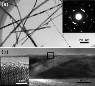
Fig. 1 shows TEM images of the SiCnanowires grown by the method outlined above. The nanowires were around 50–100 nm in diameter. The structure was cubic with numerous stacking faults. TEM images confirmed that no graphite layers were formed on the surface of the nanowires.
 | ||
| Fig. 1 (a) TEM image of as-grown SiCnanowires dispersed on a TEM microgrid. Inset: electron diffraction pattern from the SiCnanowires. (b) High-magnification TEM image of a SiCnanowire. Inset: lattice-resolved image. | ||
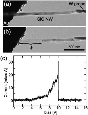
By applying a current on the order of 10 μA with a bias voltage of around 10 V, electrical breakdown occurred in the SiCnanowires that induced the transformation into CNTs or CNT-sheathed nanowires. Representative TEM images of a nanowire before and after the transformation are shown in Fig. 2(a) and (b), respectively, where the bias voltage was increased with a rate of 1 V s−1. These images were picked up from a movie (see the ESI† ). However, the transformation of the nanowires was faster than the 1 frame/s time resolution of the image recording. The I–V curve measured during the transformation is plotted in Fig. 2(c), where the maximum bias voltage and the current were about 10 V and 30 μA, respectively. The current dropped to zero presumably due to the breakdown of the contact between the nanowire and the electrode. It is worth noting that the current increased abruptly just before the breakdown from about 15 to 30 μA. This indicates that the abrupt increase in current was caused by the formation of the nanotube that is highly electrically conductive. Better time resolution is required in future studies to reveal the structural change during the transformation. We also observed another bend in the I–V curve at around 7.5 V. The movie does not show any structural change, therefore, it is likely that the bend was due to a change of contact between the nanowire and the electrode.
 | ||
| Fig. 2 In situ TEM observation of the transformation of a SiCnanowire into a nanotube. (a) Before and (b) after the transformation. The transformed part is indicated by an arrow. (c) I–V curve measured during the transformation. | ||
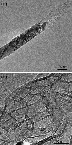
In Fig. 3, we show an example of a close-view observation in which the transformation was partial along the axial direction. The formed nanotube in Fig. 3(b) is heavily distorted and multi-walled. Its interlayer distance is measured to be about 3.5 Å, which is consistent with the interlayer distance of graphite and multi-walled CNTs. These TEM observations reveal that the formed nanotubes are CNTs.
 | ||
| Fig. 3 TEM images of a SiCnanowire converted partly to multi-walled CNT. (a) Low-magnification image and (b) a high-resolution image of the formed CNT. The interlayer distance of the CNT is about 3.5 Å. | ||
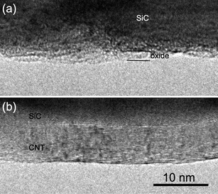
CNT formation on the surface of SiCnanowires without the disappearance of SiC cores was also observed as shown in Fig. 4. The as-grown SiCnanowire was covered inhomogeneously with an oxide layer of a few nm thickness. After Joule heating, the surface of the SiCnanowire was covered with a CNT sheath of about 7 nm thickness. No oxide intermediate layer was found between the SiCnanowire and the CNT sheath. It is worth noting that the formed CNT sheath was much thicker than the surface oxide layer of the as-grown nanowire. This reveals that the phenomenon is conducted by the simple thermal decomposition of the SiC surface followed by the evaporation of Si. It also reveals that the reaction
| SiC (solid) + SiO2 (solid) → C (solid) + 2SiO (vapor) | (1) |
 | ||
| Fig. 4 Transformation of a SiCnanowire into a SiC–CNT coaxial nanowire. TEM images (a) before and (b) after Joule heating. After the Joule heating, a thick graphite sheath was formed, and the SiC core remained. The interlayer distance of the sheath is about 3.5 Å. | ||
Li et al. have reported the direct formation of SiC–SiO2–CNT coaxial nanowires, where an intermediate oxide layer was sandwiched between a SiC core and a CNT sheath.15 In their work, annealing the coaxial nanowires at 1600 °C resulted in the transformation of the nanowires into SiC–CNT heterojunctions in which SiC and hollow CNT fragments were connected to form a chain-like structure along the axial direction. We may note that the CNT sheaths already existed in their as-grown nanowires. They attributed the transformation into hollow CNT fragments to the full reaction of the SiC cores with the surrounding intermediate oxide, which is
| SiC (solid) + SiO2 (solid) → SiO (vapor) + CO (vapor) | (2) |
On the other hand, the intermediate oxide layers and the CNT sheaths around the remaining SiC cores had been lost after the annealing in some parts to form the SiC fragments. They suggested the following reaction to explain the loss of the CNT/oxide sheath and the formation of the SiC fragments:15
| C (solid) + SiO2 (solid) → SiC (solid) + CO (vapor) | (3) |
In their nanowire growth process, the oxide played an important role, in contrast to our study. It would be interesting to investigate the effect of Joule heating on a SiCnanowire with a thick surface oxide; however, the thick surface oxide prevents us from applying an electric current because of its insulating nature.
We estimated the temperature of a nanowire during the transformation process. In the calculation, we took the power from the Joule heating, thermal radiation of the nanowire, and the thermal conduction to the electrodes into account. If these three are at the equilibrium, we obtain:
 | (4) |
![[hair space]](https://www.rsc.org/images/entities/char_200a.gif) 000 K. This temperature is higher than the melting point of C, 3800 K. Therefore, the accrual temperature must be lower than that obtained in our estimation. In our model, we assume that the thermal contacts to the electrodes are the surface oxide of the SiCnanowire; however, once the graphite layers are formed on the surface of the nanowire owing to the Joule heating, thermal conduction should be improved drastically, since the thermal conductance of a CNT is as large as ∼1000 W m−1K−1.16 Accordingly, the formation of the CNT sheath can lower the temperature. These discussions lead us to the conclusion that the temperature is below ∼10
000 K. This temperature is higher than the melting point of C, 3800 K. Therefore, the accrual temperature must be lower than that obtained in our estimation. In our model, we assume that the thermal contacts to the electrodes are the surface oxide of the SiCnanowire; however, once the graphite layers are formed on the surface of the nanowire owing to the Joule heating, thermal conduction should be improved drastically, since the thermal conductance of a CNT is as large as ∼1000 W m−1K−1.16 Accordingly, the formation of the CNT sheath can lower the temperature. These discussions lead us to the conclusion that the temperature is below ∼10![[hair space]](https://www.rsc.org/images/entities/char_200a.gif) 000 K owing to the cooling effect of CNTs, and on the 1000 K order.
000 K owing to the cooling effect of CNTs, and on the 1000 K order.
In summary, we have found that a SiCnanowire can be transformed into a CNT and a SiC–CNT core–sheath nanowire by applying an electric current, and observed the process by means of in situTEM. A simple temperature estimation revealed that the Joule heating is sufficient for thermal decomposition of SiC and formation of a CNT. SiC is a wide-bandgap semiconductor and has various excellent properties such as high electron mobility, high thermal conductivity, and high tolerance to electrical breakdown. Therefore SiCnanowires are expected to be used for fabricating nanowire-based devices that can work at high temperatures, at high power, at high frequency, and so on. Accordingly, it is important to reveal transport properties and tolerance to current for SiCnanowires. This paper also provides information on the available maximum current when using freestanding SiCnanowires as a building blocks for devices and interconnections.
This work was supported in part by a Grant-in-Aid for Scientific Research in a Priority Area Post Scaling Technology No. 18063014 from the Ministry of Education, Culture, Sports, Science and Technology, Japan. This work was also performed under the inter-university cooperative research program of the Institute for Materials Research, Tohoku University.
References
- A. J. van Bommel, J. E. Crombeen and A. van Tooren, Surf. Sci., 1975, 48, 463 CrossRef.
- Th. Seyller, K. V. Emtsev, K. Gao, F. Speck, L. Ley, A. Tadich, L. Broekman, J. D. Riley, R. C. G. Leckey, O. Rader, A. Varykhalov and A. M. Shikin, Surf. Sci., 2006, 600, 3906 CrossRef CAS.
- C. Riedl, U. Stake, J. Bernhardt, M. Franke and K. Heinz, Phys. Rev. B: Condens. Matter Mater. Phys., 2007, 76, 245406 CrossRef.
- S. V. Morozov, K. S. Novoselov, M. I. Katsnelson, F. Schedin, D. C. Elias, J. A. Jaszczak and A. K. Geim, Phys. Rev. Lett., 2008, 100, 016602 CrossRef CAS.
- M. Kusunoki, J. Shibata, M. Rokkaku and T. Hirayama, Jpn. J. Appl. Phys., 1998, 37, L605 CrossRef CAS.
- M. Kusunoki, T. Suzuki, T. Hirayama, N. Shibata and K. Kaneko, Appl. Phys. Lett., 2000, 77, 531 CrossRef CAS.
- H. Watanabe, Y. Hisada, S. Mukainakano and N. Tanaka, J. Microsc., 2001, 203, 40 CrossRef CAS.
- H. Kohno and S. Takeda, Appl. Phys. Lett., 1998, 73, 3144 CrossRef CAS.
- H. Kohno and S. Takeda, e-J. Surf. Sci. Nanotechnol., 2005, 3, 131 Search PubMed.
- T. Nogami, Y. Ohno, S. Ichikawa and H. Kohno, Nanotechnology, 2009, 20, 335602 CrossRef CAS.
- H. Kohno and H. Yoshida, Phys. Rev. E: Stat., Nonlinear, Soft Matter Phys., 2004, 70, 062601 CrossRef.
- H. Kohno and H. Yoshida, Solid State Commun., 2004, 132, 59 CrossRef CAS.
- H. Yoshida, H. Kohno, S. Ichikawa, T. Akita and S. Takeda, Mater. Lett., 2007, 61, 3134 CrossRef CAS.
- H. Kohno, H. Yoshida, S. Ichikawa and S. Takeda, J. Phys. Soc. Jpn., 2009, 78, 044601 CrossRef.
- Y. Li, Y. Bando and D. Golberg, Adv. Mater., 2004, 16, 93 CrossRef CAS.
- P. Kim, L. Shi, A. Majumdar and P. L. McEuen, Phys. Rev. Lett., 2001, 87, 215502 CrossRef CAS.
Footnote |
| † Electronic supplementary information (ESI) available: Video of the transformation monitored in situ by transmission electron microscopy. See DOI: 10.1039/b9nr00163h |
| This journal is © The Royal Society of Chemistry 2009 |
