Fabrication and characterization of polymer insulated carbon nanotube modified electrochemical nanoprobes†
Amol V.
Patil‡
a,
Anne F.
Beker
a,
Frank G. M.
Wiertz
b,
Hendrik A.
Heering
b,
Giacomo
Coslovich
a,
Rifka
Vlijm
a and
Tjerk H.
Oosterkamp
*a
aLION, Leiden University, Niels Bohrweg 2, 2333CA, Leiden, The Netherlands. E-mail: oosterkamp@physics.leidenuniv.nl
bLeiden Institute of Chemistry, Leiden University, Einsteinweg 55, 2333CC, Leiden, The Netherlands
First published on 23rd February 2010
Abstract
Electrochemical nanoprobes were fabricated from polymer insulated multiwalled carbon nanotube modified tapping mode atomic force microscope probes. An electrochemically active length of carbon nanotube was exposed by laser ablation of the insulating polymer. Characterization of these probes is done by cyclic voltammetry of ferrocenemethanol in an aqueous solution and by finite element analysis. The fabricated nanoelectrodes were found to be stable and yielded an interfacial electron transfer rate constant (k0) of 1.073 ± 0.36 cm s−1 for ferrocenemethanol.
Introduction
Investigation of electrochemical phenomena using electrodes of nanometre size has been receiving increasing attention. Reducing the geometric dimensions increases the relative mass transport rate which yields high current densities coupled with small capacitances and reduced Ohmic drop. Researchers have exploited these attributes to measure the kinetics of fast electron transfer reactions, to detect single molecules, to probe neurochemical microenvironments and as scanning electrochemistry probes.1–3Nanoelectrodes are commonly fabricated by electrochemical etching and polishing of a platinum wire or carbon fibers followed by insulating all but the very apex of the probe with a variety of insulation materials such as electrophoretic paint, molten wax or polyphenol.4 Another method for nanoelectrode fabrication consists of stretching borosilicate capillaries containing a metal wire.3,5 Recently Dekker and co-workers presented methods for on chip lithographic fabrication of nanoscopic gold6,7 and carbon nanotube (CNT) electrodes with well defined geometry.8 Although these published methods produce excellent nanoelectrodes, the methods of fabrication and resultant electrodes are difficult to integrate with an AFM probe.
In this article we present a simple and reproducible fabrication method of a fully exposed cylindrical nanoelectrode from a single insulated multiwalled CNT mounted on an atomic force microscopy (AFM) probe. The resulting probe combines the high topographical resolution achieved by a CNT modified AFM probe9,10 and the advantages of a small electrochemical electrode, which allows one to probe fast electrode kinetics by reducing the effect of diffusion and, if a short nanotube is used, improves the spatial SECM resolution.11 The advantages of using carbon as an electrode material are its wide electrochemical window and flexible surface properties which are accessible through various chemical12 and electrochemical modifications.13 To characterize the electrode kinetics of the fabricated nanoelectrodes we have made use of finite element (FE) analysis to simulate the diffusion conditions present on the surface of a nanotube and its dependence upon the geometry.
Results and discussion
Fabrication of the electrodes
A single arc discharge grown multiwalled CNT (nominal radius 10 nm, lengths ranging from 2 to 5 microns) was mounted on a gold coated tapping mode AFM cantilever in a scanning electron microscope (FEI Nova 200 NanoSEM) using a custom built manipulator assembly.14 The electrical contact resistance between the CNT and sputter coated gold surface was measured in situ and was found, typically, to be in the range of few hundred kΩ.The entire probe was insulated by a layer of chloro-p-xylylene (Parylene C) in a home built deposition system. The conformal pinhole free nature of the Parylene film depends upon the chemical nature of the substrate.15 On gold, thin Parylene layers (<500 nm) are not pinhole free. At the same time thick insulating Parylene layers are unacceptable, for our purpose, as on short length of CNT such layers would deteriorate any expected topographical imaging advantage gained from the intrinsic high aspect ratio of CNT. We have developed a simple but effective method to overcome the discongruity in the chemical nature of the CNT and gold, by passivating the gold surface with alkanethiol chemistry. By exposing a CNT modified gold probe to fumes of 1-hexadecanethiol for a period of 10 h prior to Parylene deposition we have achieved pinhole free insulation with layers as thin as 175 nm.
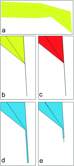
Lengths of electroactive CNT were exposed by laser ablation of the insulating polymer, as shown in Fig. 1. Details of the method employed can be found elsewhere.16
 | ||
| Fig. 1 (a) AFM cantilever with sputter-deposited gold. (b) Multiwall carbon nanotube mounted on the AFM tip. (c) Adhesion layer of alkanethiol bound to the gold surface. (d) Thin Parylene layer coating the probe. (e) End of the nanotube exposed via laser ablation. | ||
Characterization by cyclic voltammetry and finite element modeling
Electrochemical characterization of the fabricated electrodes was carried by studying oxidation of ferrocenemethanol by cyclic voltammetry. This was performed with a homebuilt low noise high resolution current to voltage (IV) converter connected to a PC via a 16 bit AD/DA converter and controlled by a LabView routine, monitoring the current from the nanoelectrodes (held at ground potential) while a triangular voltage signal was applied to an Ag/AgCl reference electrode, in a two electrode setup. The entire experiment was carried out in a Faraday cage, in which nanoprobes were dipped inside the ferrocenemethanol solution up to the AFM cantilever. All experimental and FE data given correspond to cyclic voltammetry of 0.2 mM aqueous solution of ferrocenemethanol (D0 = 7.8 × 10⁻¹⁰ m2 s−1, E0 = 0.219 V vs. Ag/AgCl electrode) with 0.1M KCl as supporting electrolyte at scan rate 0.1 V s−1, at room temperature.We observed a steady-state electrochemical current through various nanoelectrodes tested. As mentioned in the Materials and methods section (below) it is important to add a plasma cleaning step on the exposed nanotubes, to obtain reproducible fabrication and voltammetry, particularly on the shorter nanotubes. The yield of the fabrication process is limited by the laser exposure step in which 50% of the parylene removal attempts are successful without destroying the carbon nanotube. The total yield is about 1 in 4 probes. At high potential, an anodic current was observed which corresponds to oxidation of ferrocenemethanol. The current varies with electroactive area with current ranging from few picoamps to tens of picoamps. During testing, the nanoelectrodes were found to be stable over 20 scans taken over a time period of 7 min. After this period, the amplitude of the diffusion limited current and of the electron transfer rate k0 reduced, which could be attributed to contaminants present in the solution, a rapid process due to fast mass transport. For longer measurements it is very important to address this contamination problem.
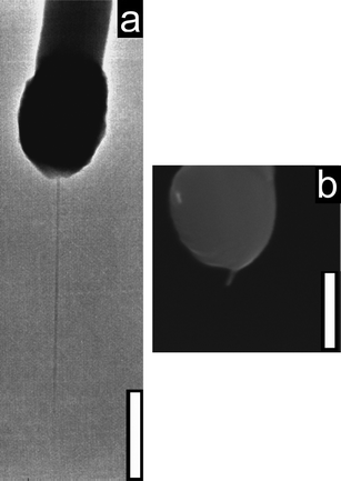
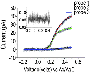
In order to characterize the behavior of the fabricated nanoelectrode, we chose three nanoelectrodes with different lengths of exposed CNT, ranging from a few hundreds of nanometres to two microns (Fig. 2), and a control probe in which no electroactive area was exposed. In Fig. 3 we show the voltammograms obtained.
 | ||
| Fig. 2 (a) TEM pictograph of a long electrode. (b) SEM pictograph of a short electrode. (Scale bars: 500 nm). | ||
 | ||
| Fig. 3 Baseline corrected averaged (5 anodic sweeps) voltammograms for three nanoelectrodes with different lengths of carbon nanotube exposed: 1770, 1240 and 118 nm. FFT low pass filter (45 Hz). Fits generated for experimental data using FE simulation (line). Inset: Control probe with non exposed carbon nanotube (pA vs. V). | ||
The fabricated nanoelectrodes have a diffusion profile which is a result of combination of hemispherical diffusion to cap and cylindrical diffusion to the sidewall. This prevents us from developing a simple equation for the Faradic current for one step, one electron process such as is available for a hemispherical electrode.
Hence, for the characterization of the electrodes, we employed FE analysis which permits simple inclusion of electrode kinetics for the heterogeneous electron transfer process as the boundary conditions for the electron flux at the CNT surface, without any predefined diffusion conditions. For the oxidation of ferrocenemethanol (FcMeOH) ka and kc, the anodic (oxidation) and cathodic (reduction) electron transfer rates, respectively, are defined as:
Where k0 is the standard rate constant, α the charge transfer coefficient, E0 the standard potential of the redox reaction17 and E the applied potential.
The current at the electrode will thus be the current density J(r,z) integrated over the electrode area:
| J(r,z) = nF(kacred − kccox) |
 | ||
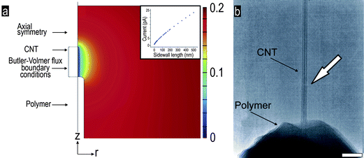
| Fig. 4 (a) FE computed reduced species concentration near the surface of nanoelectrode (radius = 20 nm, α = 0.675, k0 = 1.45 cm s−1, E = 0.5 V). Inset: FE computed steady-state current for our nanoelectrode geometry: radius = 10 nm, α = 0.66, k0 = 1.52 cm s−1, E = 0.5 V, and varying lengths of the CNT sidewall. (b) TEM pictograph of the exposed CNT (white arrow pointing at the residual polymer layer). Scale bar: 50 nm. | ||
The net Faradic current was calculated for a single potential sweep (from −0.2 V to 0.5 V applied to the working electrode and n = 1). Dimensions of the polymer thickness, nanotube radius and estimated bare length were determined by SEM.
In order to understand the effect of aspect ratio on diffusion profile, we varied the length of the cylinder (with fixed radius value of 10 nm). For lengths larger than 200 nm the net Faradic current scaled approximately linearly with the length of the cylinder (see inset Fig. 4). This compares well with the findings of Crooks et al.18 on nanotubular electrodes dipped in an electrolyte at several immersion depths. As expected, the simulations showed that a 10 nm section of cylinder just below the tip contributes more to the total current than a 10 nm section of cylinder that is further down. This is because the spherical geometry of the end shows a different diffusion behavior than the cylindrical geometry of the sidewall. This causes the concentration gradients to be different on different parts of the nanoelectrodes, as shown in Fig. 4(a). Furthermore, at longer distance the concentration profile rapidly tends towards a gradient obtained for spherical diffusion, increasing the net mass flux towards the electrode surface. This yields a steady-state, unlike the quasi steady-state obtained for pure cylindrical diffusion.19
The electroactive surface area, heterogeneous rate constant and transfer coefficient were reasonably estimated by fitting the experimental data to a curve generated by the FE simulation, as shown in Fig. 3. The computed values for k0, the standard rate constant and α, the charge transfer coefficient are listed in Table 1. The electro active length predicted by FE simulation was found to be approximately equal to or smaller than the apparent length seen in SEM, a good confirmation that there were no leaks in the insulating polymer layer on the rest of the micron sized AFM cantilever. The smaller electroactive length (than apparent length determined by SEM) can be explained by the presence of thin residual layer of polymer, which cannot be detected by SEM, on the exposed carbon nanotube away from the distal end as shown in Fig. 4(b). Such a thin residual layer will change the diffusion profile near the base of CNT, allowing for higher diffusion flux values towards the base, as compared to the diffusion profile computed by the FE model which assumes a flat polymer surface normal to a clean electrode with uniform k0 over the entire electroactive surface.
The average k0 calculated by FE was 1.073 ± 0.36 cm s−1, a value that can be compared to 2.06 ± 0.31 cm s−1 reported on platinum microelectrodes20 and around 1 cm s−1 measured recently21 on a glassy carbon electrode. It is higher than the value of approximately 0.2 cm s−1 measured on larger glassy carbon22 and gold electrodes,23 but lower than the k0 values reported recently on gold SECM tips.24 Our findings that not only are the fitted lengths consistent with the lengths measured by SEM but also the k0 are consistent with each other further confirms the earlier suggestion that the estimated electroactive area is correct, i.e. no pinholes are present in the insulation layer, as any underestimation of electroactive area leads to overestimation of rate constants. Thus with our fabricated nanoelectrodes, upon characterization, we have reliable knowledge of the geometric structure and electrode kinetics. Since our nanoelectrodes are essentially a CNT modified AFM probe, they can be employed as a composite AFM/scanning electrochemistry probe utilizing the topographical resolution of a carbon nanotube modified AFM probe and electrochemical resolution of a nanoelectrode. Longer nanotubes can be employed for imaging after shortening.10,25
Conclusion
In conclusion a simple reliable fabrication method of nanoelectrodes has been demonstrated. We have presented a simple finite element analysis model which computes the electrode kinetics of the cylindrical nanoprobes. The nanoprobes were found to be stable, with an estimated interfacial electron transfer rate of 1.073 ± 0.36 cm s−1 for ferrocenemethanol. In the future, we intend to use these high aspect ratio nanoelectrodes as SECM and conductive AFM probes with very high electrochemical and topographical resolution.Materials and methods
Materials
Tapping mode AFM cantilevers used in above work were purchased from Olympus (AC240TS, nominal resonant frequency 80 kHz) and were sputter coated with 5 nm of molybdenum–germanium followed by 70 nm of gold. Chloro-p-xylylene (Parylene C®) was obtained from Specialty Coating Systems, while ferrocenemethanol, 1-hexadecanethiol & potassium chloride were purchased from Sigma Aldrich. All solutions were prepared in deionized water (18 MΩ cm Milli-Q, Millipore). The reference electrode used in all experiments was Ag/AgCl/3 M NaCl (BAS RE-5B, +0.215 V vs. NHE, purchased from Bioanalytical Systems).Electrode fabrication
Various lengths of carbon nanotube, ranging from a few tens of nanometres to a micron, were exposed by removing Parylene from the probing end. This was achieved by controlled introduction into the focal spot of a plane polarized continuous wave green laser (50 mW, Nd: YAG, 532 nm) of the polymer coated carbon nanotube, thus heating the selected length. This causes the thermoplastic polymer to “ball up” away from the heated length. After laser treatment, the probe was imaged with a SEM to measure the length and the radius of the exposed carbon nanotube. To clean any remaining parylene or amorphous carbon layer that might have deposited during high magnification SEM imaging, the probes were exposed to an oxygen plasma for a short time duration (sufficient to clean a thin layer of amorphous carbon while not creating pinholes in the insulating polymer layer, typically 10 s in Oxford Plasmalab 90+ plasma etcher).Finite element modeling
Since the simulation cannot be computed for infinite volume of the electrolyte, we ensured that the maximum cell dimension (zmax) value has a much larger value than the maximum diffusion layer thicknessWhere t is the time required to finish a single linear sweep.26 The spatial and temporal accuracy of the formulated mathematical model was verified by applying the Butler–Volmer model with reaction rate equations as boundary conditions for a hemispherical electrode for which an analytical solution for the diffusion mass transport equation exists.
We observed a very good agreement between the FEM and analytical solution (data not shown) leading to the conclusion that the current simple FEM model gives reasonably correct values for the normal diffusive flux (with error ≤0.77%).
For the cap of the carbon nanotube we use the same k0 as for the sidewalls even though we observe that the laser treatment, which is performed in air, shortens the carbon nanotubes.
To allow a reasonably quick convergence of the fitting procedure, we first keep the length constant at the value measured by SEM. After the curve is fitted with k0 and α, we iteratively allow all three parameters to change.
Acknowledgements
We thank Prof. Andrew Rinzler, Department of Physics, University of Florida for supplying the multiwalled carbon nanotubes which were used in this work and Dr F. D. Tichelaar, National Centre for HREM at TU Delft, for TEM imaging of the nanoelectrodes. This work was financed by Technologiestichting STW. HAH and FGMW are financially supported by the Netherlands Organization for Scientific Research (NWO).Notes and references
- R. W. Murray, Chem. Rev., 2008, 108, 2688–2720 CrossRef CAS.
- F. J. M. Hoeben, F. S. Meijer, C. Dekker, S. P. J. Albracht, H. A. Heering and S. G. Lemay, ACS Nano, 2008, 2, 2497–2504 CrossRef CAS.
- S. Amemiya, A. J. Bard, F. R. F. Fan, M. V. Mirkin and P. R. Unwin, Annu. Rev. Anal. Chem., 2008, 1, 95–131 Search PubMed.
- D. W. M. Arrigan, Analyst, 2004, 129, 1157–1165 RSC.
- B. B. Katemann and T. Schuhmann, Electroanalysis, 2002, 14, 22–28 CrossRef CAS.
- D. Krapf, M. Y. Wu, R. M. M. Smeets, H. W. Zandbergen, C. Dekker and S. G. Lemay, Nano Lett., 2006, 6, 105–109 CrossRef CAS.
- S. G. Lemay, D. M. van den Broek, A. J. Storm, D. Krapf, R. M. M. Smeets, H. A. Heering and C. Dekker, Anal. Chem., 2005, 77, 1911–1915 CrossRef CAS.
- I. Heller, J. Kong, H. A. Heering, K. A. Williams, S. G. Lemay and C. Dekker, Nano Lett., 2005, 5, 137–142 CrossRef CAS.
- S. S. Wong, E. Joselevich, A. T. Woolley, C. L. Cheung and C. M. Lieber, Nature, 1998, 394, 52–55 CrossRef CAS.
- H. J. Dai, J. H. Hafner, A. G. Rinzler, D. T. Colbert and R. E. Smalley, Nature, 1996, 384, 147–150 CrossRef CAS.
- D. P. Burt, N. R. Wilson, J. M. R. Weaver, P. S. Dobson and J. V. Macpherson, Nano Lett., 2005, 5, 639–643 CrossRef CAS.
- J. Li, J. E. Koehne, A. M. Cassell, H. Chen, H. T. Ng, Q. Ye, W. Fan, J. Han and M. Meyyappan, Electroanalysis, 2005, 17, 15–27 CrossRef CAS.
- X. R. Ye, L. H. Chen, C. Wang, J. F. Aubuchon, I. C. Chen, A. I. Gapin, J. B. Talbot and S. Jin, J. Phys. Chem. B, 2006, 110, 12938–12942 CrossRef CAS.
- E. C. Heeres, A. J. Katan, M. J. van Es, A. F. Beker, M. Hesselberth, D. J. van der Zalm and T. H. Oosterkamp, Rev. Sci. Instrum., 2010, 81, 023704 CrossRef.
- K. M. Vaeth and K. F. Jensen, Chem. Mater., 2000, 12, 1305–1313 CrossRef CAS.
- A. Patil, J. Sippel, G. W. Martin and A. G. Rinzler, Nano Lett., 2004, 4, 303–308 CrossRef CAS.
- A. J. Bard and L. R. Faulkner, Electrochemical Methods: Fundamentals and Applications, 2nd ed., John Wiley & Sons, New York, 2000 Search PubMed.
- J. K. Campbell, L. Sun and R. M. Crooks, J. Am. Chem. Soc., 1999, 121, 3779–3780 CrossRef CAS.
- A. Szabo, D. K. Cope, D. E. Tallman, P. M. Kovach and R. M. Wightman, J. Electroanal. Chem. Interfacial Electrochem., 1987, 217, 417–423 CrossRef CAS.
- W. J. Miao, Z. F. Ding and A. J. Bard, J. Phys. Chem. B, 2002, 106, 1392–1398 CrossRef CAS.
- A. P. O'Mullane, J. Zhang, A. Brajter-Toth and A. M. Bond, Anal. Chem., 2008, 80, 4614–4626 CrossRef CAS.
- C. Bourdillon, C. Demaille, J. Moiroux and J. M. Saveant, J. Am. Chem. Soc., 1995, 117, 11499–11506 CrossRef CAS.
- C. Cannes, F. Kanoufi and A. J. Bard, J. Electroanal. Chem., 2003, 547, 83–91 CrossRef CAS.
- J. Velmurugan, P. Sun and M. V. Mirkin, J. Phys. Chem. C, 2009, 113, 459–464 CrossRef CAS.
- A. J. Katan and T. H. Oosterkamp, J. Phys. Chem. C, 2008, 112, 9769–9776 CrossRef CAS.
- H. A. Heering and W. R. Hagen, J. Electroanal. Chem., 1994, 364, 235–240 CrossRef CAS.
Footnotes |
| † Electronic supplementary information (ESI) available: Details of the finite element model. See DOI: 10.1039/b9nr00281b |
| ‡ Current address: Chemical Research Laboratory, University of Oxford, South Parks Road, Oxford, OX13TA, UK. E-mail: E-mail: amol.patil@chem.ox.ac.uk |
| This journal is © The Royal Society of Chemistry 2010 |


