Non-square-well potential profile and suppression of blinking in compositionally graded Cd1−xZnxSe/CdxZn1−xSe nanocrystals
Andrew Das
Arulsamy
*ab,
Uros
Cvelbar
b,
Miran
Mozetic
b and
Kostya (Ken)
Ostrikov
*ac
aSchool of Physics, The University of Sydney, Sydney, New South Wales 2006, Australia. E-mail: sadwerdna@gmail.com
bJožef Stefan Institute, Jamova cesta 39, SI-1000, Ljubljana, Slovenia
cCSIRO Materials Science and Engineering, P.O. Box 218, Lindfield, New South Wales 2070, Australia. E-mail: Kostya.Ostrikov@csiro.au
First published on 5th February 2010
Abstract
Random blinking is a major problem on the way to successful applications of semiconducting nanocrystals in optoelectronics and photonics, which until recently had neither a practical solution nor a theoretical interpretation. An experimental breakthrough has recently been made by fabricating non-blinking Cd1−xZnxSe/ZnSe graded nanocrystals [Wang et al., Nature, 2009, 459, 686]. Here, we (1) report an unequivocal and detailed theoretical investigation to understand the properties (e.g., profile) of the potential-well and the distribution of Zn content with respect to the nanocrystal radius and (2) develop a strategy to find the relationship between the photoluminescence (PL) energy peaks and the potential-well due to Zn distribution in nanocrystals. It is demonstrated that the non-square-well potential can be varied in such a way that one can indeed control the PL intensity and the energy-level difference (PL energy peaks) accurately. This implies that one can either suppress the blinking altogether, or alternatively, manipulate the PL energy peaks and intensities systematically to achieve a controlled non-random intermittent luminescence. The approach developed here is based on the ionization energy approximation and as such is generic and can be applied to any non-free-electron nanocrystals.
1. Introduction
Quantum dots (QDs) in all fields of applications have one intrinsic problem—they blink randomly. Blinking is defined by intensity fluctuations in nanocrystals (NCs) or QDs, which is due to intermittent photoluminescence (PL) under continuous photoexcitation.1 This blinking effect is due to the fluctuations of PL from an ensemble of individual NCs. In other words, the excited electrons radiatively recombine with holes at different rates in individual NCs. Such discontinuous PL causes some of the QDs to be switched-on (emission) while others remain switched-off (due to trapped electrons or holes and also due to the non-radiative Auger process).1–3 The trapped electrons have relatively large recombination lifetimes, which vary from one NC to another in an ensemble of NCs. The blinking effect was first observed and reported by Nirmal et al.,4 and has been discussed extensively since then.5–8 Interested readers are referred to ref. 8 for a thorough review on the blinking effect.These discontinuous emissions are indeed undesirable for solar cells, nano-electronics and biological applications. Hence, one needs to fine-tune the electronic properties of the QDs so as to avoid blinking in the QDs.1 These random and intermittent emissions in a single NC, that give rise to the blinking effect, have been suppressed recently by custom-designing a compositionally graded CdZnSe/ZnSe core/shell structure.1 These graded structures have given rise to a series of smaller energy levels for the excited electrons to recombine at a faster rates within the NCs, which in turn resulted in quasi-continuous emission. Therefore, further theoretical work need to be carried out to understand (I) why such compositionally graded structures have increased the recombination rates and (II) how one can further improve the grading and the electron confinement in other material systems and core/shell structures to eliminate the blinking effect.
Apart from the non-blinking effect, points (I) and (II) stated above are also crucial to the advancement of nanotechnologies in different fields such as renewable energy, nano-electronics and biomedicine. For example, one of the straightforward applications of QDs is in photovoltaic solar cells. In this application, one does not need to control the size and spatial distribution of QDs accurately since one can achieve an energy gap distribution arising from the size non-uniformity of QDs. In fact, such non-uniformity enables effective photon energy absorption (between 0.5 to 3.5 eV) from the sunlight.9–11 However, the carrier multiplication is not effectively enhanced even in the presence of high energy photons.12,13 Meanwhile, studies of the electron confinement and PL in Si nanostructures14–16 reveal that small Si-based QDs absorb higher-energy photons, whereas larger QDs absorb photons with lower energy. Clearly, fluctuating recombination rates in these QDs are undesirable for a continuous photovoltaic power source. On the other hand, QD research fields related to biological applications are also emerging and expanding exponentially,17,18 where QDs have been successfully used as bio-probes19 and also in biological imaging.20,21 Such biological applications give rise to the need to study the effect of QD chemical properties and their nanoscale size on health and environment, which have been pointed out and emphasized in recent years.20,22–25 Many of the physical phenomena that enable such applications are essentially based on the points (I) and (II) above.
Here, we will analyze and understand the variation of the energy-level spacing responsible for the non-blinking effect in the Cd1−xZnxSe/ZnSe NCs with respect to Zn content, x (elemental composition). Our objectives to achieve points (I) and (II) mentioned above are (a) to re-interpret the experimental results reported in ref. 1, and (b) to make experimentally viable predictions for similar effects in other quantum dot and materials systems. The analysis presented here will also enable one to predict the PL spectra for the core/shell structure of ZnSe/Cd1−xZnxSe NCs, an inverse NC structure as compared to CdZnSe/ZnSe.1 In (a) we will attempt to interpret the experimentally measured PL intensities and the energy peaks as a function of Zn content (x). We will also develop generic guidelines on the suppression of blinking effects in multi-element nanocrystals made of non-free-electron materials.
The paper is organized as follows. The details of our model with respect to the ionization energy theory (IET) are given in Section 2. In Section 3, we present the detailed analysis on the Cd1−xZnxSe/ZnSe nanocrystals. In Section 4, we discuss and make predictions on the ZnSe/Cd1−xZnxSe, an inverse core/shell structure of Cd1−xZnxSe/ZnSe nanocrystal. The analysis in Section 5 focuses on the effect of grading-depth due to inhomogeneous Zn concentration in these NCs. In addition, we also evaluate the possibility of achieving the sufficient grading-depth for other well-known systems, namely, CdSe/ZnS and InGaAs/GaAs. The paper ends with a brief concluding section, where the main results are summarized.
2. Model
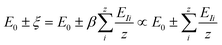
Our model for describing the potential wells in elementally graded NCs is based on the IET, which relates the atomic ionization energy of the constituent atoms to the energy level difference of NCs. The Schrödinger equation for the IET is given by26| Ĥφ = (E0 ± ξ)φ | (1) |
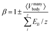
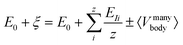
The microscopic and mathematical details of the Hamilton operator, Ĥ and the IET can be found in ref. 27. The exact eigenvalue is given by E0 ± ξ, where E0 is the total energy of the system at zero temperature (T = 0 K) and ξ is the energy-level difference (also called the ionization energy) in a given NC, which is equivalent to the energy peak positions in the PL spectra. By identifying ξ as the real energy level difference in NCs and EI as the average atomic energy level differences (averaged from all the constituent atoms in NCs), one can write the eigenvalue in eqn (1) as
 | (2) |
 | (3) |
 | (4) |
It is clear that ξ ≥ EI is valid for β ≥ 1, while ξ < EI is valid for 0 < β < 1. In the subsequent analysis, eqn (2)–(4) will be used to interpret the PL spectra for Cd1−xZnxSe/ZnSe NCs. For example, eqn (4) indicates that E0 and 〈Vmanybody〉 are material-specific constants for one given composition, and any changes to the composition by varying the Zn content, x can be directly related to EI. Therefore, any changes to the elemental composition can be related to the EI and, subsequently, to the intensities and energy peak positions in the PL spectra.
3. Analysis I: Cd1−xZnxSe/ZnSe
Fig. 1A indicates the expected profile of the graded potential (almost a parabolic well) as measured in ref. 1 for a Cd1−xZnxSe/ZnSe core/shell NC structure. The data from PL spectra reported by Wang et al.1 can be written in such a way that the PL spectra satisfy two conditions, (i) P1 > P2 > P3 and (ii) P1 − P2 < P2 − P3, where P denotes the measured PL energy peak positions. We also label the PL peak intensities as I1, I2 and I3, respectively. We now interpret the intensity, I1 for the PL peak P1, which corresponds to the Zn content x1; in other words, x1 ∝ I1, x2 ∝ I2 and x3 ∝ I3. Hence, our interpretation reads, x1 = 1.00 ∝ I1, x2 = 0.87 ∝ I2 and x3 = 0.26 ∝ I3, see Fig. 1A for details. The values 1.00, 0.87 and 0.26 are the normalized PL intensities imported from ref. 1.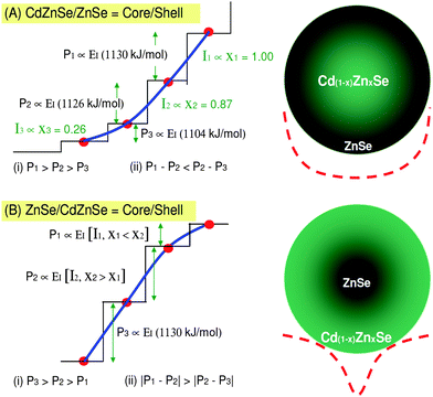 | ||
| Fig. 1 Panel (A) shows the one-half potential (solid line) for the core/shell structure, CdZnSe/ZnSe. The step-like feature represents the actual discrete energy levels in the nanocrystals. Panel (B) shows the expected one-half potential well if we were to have ZnSe/CdZnSe as core/shell, i.e., the inverse structure of panel (A). The full potential profiles are drawn with dashed lines for both (A) and (B). Both panels A and B show the sketches of the confining potentials for the respective NCs; there is only one confining potential for each graded or ungraded NC. Therefore, the three different peaks correspond to the three different values of the energy-level spacing within the same confining potential rather than three different confining potentials. These schematic diagrams are not to scale. | ||
Conditions (i) and (ii), after invoking the IET, give rise to the potential-well profile shown in Fig. 1A. Note here that we only show the one-half of the potential well for convenience. The step-like feature in Fig. 1A is entirely due to the changes in the ionization energy (energy-level spacing) as a result of changing x with radius, r, (x(r)) of the NC from the center (r = r0 = 0) or from the outer surface (r = rNC). This step-like (discrete energy levels) feature can be represented with a continuous solid line given in Fig. 1A that represents the one-half of the potential well (the full potential profiles are denoted with dashed lines).
Recall here that in contrast to ref. 1, we did not assume P1 − P2 = P2 − P3 because this assumption would not be consistent with the results of the PL measurements for all the NCs studied in ref. 1. This experiment, as well as our IET model, suggests that the emission from all the NCs always satisfies P1 − P2 < P2 − P3. Indeed, the difference between the peak positions P1 − P2 and P2 − P3 is quite different in our model and the experiment. This difference may be due to the qualitative nature of the IET approximation and values of the ionization energy used. Nonetheless, what is most important here is that both sets of data do satisfy the essential condition P1 − P2 < P2 − P3 and as such, are consistent.
The ionization energy (see Table 1) for the ZnSe shell (EIshell) can be approximated (ionization energy approximation26,27) as EIshell = ½Zn + ½Se = ½(1320) + ½(941) = 1130 kJ mol−1. On the other hand, the ionization energy for the core, Cd1−xZnxSe is EIcore = ½[(x)Zn + (1 − x)Cd] + ½Se. Therefore, for x1 = 1.00, EIshell = EIcore = 1130 kJ mol−1, for x2 = 0.87, EIcore = ½[(0.87)(1320) + (0.13)(1250)] + ½(941) = 1126 kJ mol−1. For x3 = 0.26, we obtain, EIcore = 1104 kJ mol−1.
| Ion | Atomic number Z | Valence state | E I /kJ mol−1 |
|---|---|---|---|
| S | 16 | 1+ | 1000 |
| Zn | 30 | 2+ | 1320 |
| Ga | 31 | 3+ | 1840 |
| As | 33 | 3+ | 1827 |
| Se | 34 | 1+ | 941 |
| Cd | 48 | 2+ | 1250 |
| In | 49 | 3+ | 1694 |
It should be noted that our model implies a continuous compositional grading within the nanocrystal and, hence, only a single and smooth confining potential. This assumption is perfectly accurate when the crystal sizes are sufficiently large and the microscopic structure of atomic layers composing the NC can be neglected. In reality, compositional grading is realized through the difference in the numbers of atoms of constituent elements from one internal shell to another. Conditions for effective photoluminescence are met in a few localized groups of such shells, which leads to the discrete luminescence peaks observed in the experiment.1 Since the number of clearly resolved peaks was three,1 we have identified the localized areas where generation of such emission is most likely. These three distinct areas are characterized by very specific values of Zn content, being x1, x2, and x3. We emphasize here that one should not interpret these specific “discrete” areas as a manifestation of non-continuous elemental composition grading.
We can now recall the PL intensities and rewrite them as functionals of x(r): I1[x1(r1)], I2[x2(r2)] and I3[x3(r3)], where r1 > r2 > r3. As a consequence, smaller intensity implies lower content of Zn or smaller x due to decreasing r (radially moving inward from the shell to the core of the NC). The existence of such functionals have been shown experimentally in YxGd1−xVO4![[thin space (1/6-em)]](https://www.rsc.org/images/entities/char_2009.gif) :Eu3+ by Wu and Yan.28 Furthermore, three-dimensional numerical simulations (for a fixed carrier density: 1022 cm−2s−1) were carried out by Benbakhti et al.29 resulting in the carrier-density dependent (or x-dependent in our case) PL intensities.
:Eu3+ by Wu and Yan.28 Furthermore, three-dimensional numerical simulations (for a fixed carrier density: 1022 cm−2s−1) were carried out by Benbakhti et al.29 resulting in the carrier-density dependent (or x-dependent in our case) PL intensities.
Consequently, one can explain the origin of conditions (i) and (ii) discussed above using the ionization energy approximation. The reason for (i) is the decreasing Zn content or x (as one moves inwards into the NC) that gives rise to decreasing ionization energies from 1130 to 1126 kJ mol−1 and then to 1104 kJ mol−1. Note here that the ionization energy is the atomic energy level difference (or the energy-level spacing). Condition (ii) is also satisfied: 1130 − 1126 = 4 kJ mol−1 = 41 meV per atom and 1126 − 1104 = 22 kJ mol−1 = 228 meV per atom, thus, 41 < 228 meV per atom. From ref. 1, condition (ii) reads P1 − P2 = 156 meV, P2 − P3 = 171 meV and therefore, 156 < 171 meV.
All the ionization energy values prior to averaging were taken from ref. 39. The IET approximation has been shown to be accurate in non-free-electron solids of any dimensions (from zero- (QD) to three-dimensional (bulk) materials) that can be used to understand the properties of strongly correlated matter.27 Furthermore, it is also worth to mention that there are reports on the growth of graded Si1−xCx, InSb and GaAs QDs via the plasma-assisted nano-assembly.30–33 In these studies, it was shown that the grading of elemental composition in the QDs can be controlled systematically. Interestingly, the plasma-assisted growth mechanism has been successfully implemented experimentally to synthesize the Si1−xCx QD arrays34 and iron oxide nanostructures.35 Further details on these experimental and numerical techniques can be found in ref. 36–38. In the following section, we will study and predict the PL properties of the ZnSe/Cd1−xZnxSe structure.
4. Analysis II: ZnSe/Cd1−xZnxSe
In previous sections, we have explained the essential experimental PL results presented in ref. 1, namely the changes of PL intensities, conditions (i) and (ii). The next step is that we need to use this information to further elaborate the approach to suppress blinking in NCs of different elemental compositions. These predictions are particularly important for the development of new and improved non-blinking nanocrystalline materials. We also propose the possibility of varying the potential well of any non-free-electron NCs and/or QDs at will by simply changing the elemental grading, x(r). The changes to this potential well can be estimated accurately by measuring the intensities, the PL energy peak positions [condition (i)] and the energy difference between the PL energy peak positions [condition (ii)].For example, we expect the potential well for the core/shell ZnSe/Cd1−xZnxSe structure (Fig. 1B) to be different compared to the core/shell structure for the Cd1−xZnxSe/ZnSe NC discussed earlier (Fig. 1A). The reason is that EIshell < EIcore, and this inequality implies that the ionization energy increases with the depth of the NC, or as one moves inwards (decreasing r) into the NC. In the case discussed earlier with the Cd1−xZnxSe/ZnSe NC, we had EIshell > EIcore. The latter inequality implies decreasing ionization energy due to decreasing Zn content as one approaches the center of the NC. Recall here that EIZn > EICd. This last inequality together with the dependence of x(r) defines the profile of the potential well in these NCs. By controlling x(r) accurately via diffusion or by any other means one should be able to control both the potential well profile and hence the strength of the electron confinement in NCs. In the following section, x(r) will be revisited with further analysis.
5. Further analysis and predictions for other nanocrystalline systems
Let us now use eqn (2)–(4) to demonstrate that the β [eqn (3)] for NCs is bounded in 0 < β < 1, in which ξ < EI. It is clear from the above discussion that the real energy level differences (ξ) in the NC, Cd1−xZnxSe/ZnSe satisfy the inequality, ξ(156 and 171 meV per NC) < EI(41 and 228 meV per atom). Therefore, eqn (4) can be rewritten as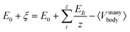 | (5) |
We can now extend our approach to other well-known systems, namely, CdSe/ZnS40,41 and InGaAs/GaAs.42Table 2 lists the averaged atomic ionization energies (EI) for four different core/shell structures, CdSe/ZnS, CdSe/ZnSe, CdZnSe/ZnSe and InGaAs/GaAs. In these structures, all the EI values for the cores are smaller than the shells, which in turn implies that these NCs, if graded, will feature the non-square-well potential similar to the one sketched in Fig. 1A (dashed line). If on the other hand, one switches the core(Y)/shell(Z) structure to core(Z)/shell(Y), then it is possible to obtain the non-square-well potential described in Fig. 1B (also labeled with a dashed line).
| core/shell NC | Core/kJ mol−1 | Shell/kJ mol−1 | |Δ|/kJ mol−1 |
|---|---|---|---|
| CdSe/ZnS | 1095 | 1160 | 65 |
| CdSe/ZnSe | 1095 | 1130 | 35 |
| CdZnSe/ZnSe | 1113 | 1130 | 17 |
| InGaAs/GaAs | 1787 | 1834 | 47 |
The second issue arising from Table 2 is the magnitude of |Δ| = |EIcore − EIshell| for different NC structures. For example, one can arrange the NC structures in the order of increasing |Δ|: CdZnSe/ZnSe (17 kJ mol−1) → CdSe/ZnSe (35 kJ mol−1) → InGaAs/GaAs (47 kJ mol−1) → CdSe/ZnS (65 kJ mol−1). One can use this information to further understand the required grading-depth (GD) to suppress the blinking effect in nanocrystals. The GD in this case can be defined as the average length of a Zn ion can diffuse into the core in a CdZnSe/ZnSe nanocrystal.
Fig. 2 shows the details of the GD for the NC based on Fig. 1B. In this case, GD = rinnershell(Cd0.5Zn0.5Se) − routercore(ZnSe), which suggests that the gradient of Zn concentration within this GD range [sandwiched between rinnershell(Cd0.5Zn0.5Se) and routercore(ZnSe)] can be large if |Δ| is made small. Otherwise, the concentration gradient has to be small. The small concentration gradient can only be achieved by having a larger GD. This latter scenario may limit the strength of the electronic confinement due to size-constraint because a large GD means a large NC size and, hence, a weak electron confinement.
![The definition of the grading-depth (GD) of a NC given in a two-dimensional diagrammatic form. Each region (separated with solid vertical lines) has different x or Zn concentration (follow the arrows pointing downward). However, the Zn-concentration gradient [x = x(r)] only exists between the core, ZnSe [fixed x = 1 below routercore(ZnSe)] and the shell, Cd0.5Zn0.5Se [fixed x = 0.5 above rinnershell(Cd0.5Zn0.5Se)]. Therefore, the radius of the NC satisfies the inequality, r0 < routercore(ZnSe) < r(Cd1−xZnxSe) < rinnershell(Cd0.5Zn0.5Se) < rNC.](/image/article/2010/NR/b9nr00322c/b9nr00322c-f2.gif) | ||
| Fig. 2 The definition of the grading-depth (GD) of a NC given in a two-dimensional diagrammatic form. Each region (separated with solid vertical lines) has different x or Zn concentration (follow the arrows pointing downward). However, the Zn-concentration gradient [x = x(r)] only exists between the core, ZnSe [fixed x = 1 below routercore(ZnSe)] and the shell, Cd0.5Zn0.5Se [fixed x = 0.5 above rinnershell(Cd0.5Zn0.5Se)]. Therefore, the radius of the NC satisfies the inequality, r0 < routercore(ZnSe) < r(Cd1−xZnxSe) < rinnershell(Cd0.5Zn0.5Se) < rNC. | ||
As such, it is relatively easy to suppress the blinking effect for a CdSe/ZnSe nanocrystal because the required GD is smaller, as compared to InGaAs/GaAs. For a InGaAs/GaAs nanocrystal, one needs In to diffuse far enough (smaller In concentration gradient) toward the shell to suppress the blinking effect due to large |Δ|. In other words, |Δ|CdSeZnSe < |Δ|InGaAsGaAs → 35 < 47 kJ mol−1. Smaller |Δ| also means shorter relaxation lifetimes, which are required to obtain a non-blinking NC as pointed out in ref. 1.
From our analysis presented above, we propose here that the origin of the blinking effect, apart from the commonly accepted trapped electrons and non-radiative processes,43 could also be due to large concentration gradients quantified by the value |Δ|. Indeed, large |Δ| implies longer relaxation lifetime as reported by Rajesh et al.7 Note here that the gradient for an ungraded NC is infinity (large |Δ|) at the interface between the core and the shell, in complete agreement with our analysis thus far. Systematic grading of the NC composition splits the single-level excitation (P ∝ |Δ|) in an ungraded NC to a smaller multi-level excitations in a graded NC. The three-level excitations shown in Fig. 1 correspond to three energy peaks, P1(I1) ∝ |Δ|1, P2(I2) ∝ |Δ|2 and P3(I3) ∝ |Δ|3. Recall here that the PL energy peak intensities (I) are related to x and therefore to EI for a given energy peak position (P), and this is how the P is related to I. This means that if x is constant, then P(I) is also constant throughout the NC. Apart from that, one should also be aware that the phonons within the NC may also significantly affect the relaxation lifetimes.44 Extensive discussion on this phonon-assisted relaxation lifetime issue within the IET is given in ref. 45. We emphasize here that our analysis based on the IET is complementary to the interpretations given in ref. 1.
We stress here that, similar to ref. 1, our model of the blinking suppression also requires a continuous compositional grading within the nanocrystal and hence, only a single and smooth confining potential. Yet it is different from ref. 1 in that the proposed mechanism relies on the emission that originates from three distinctive regions (within the nanocrystals) with different composition and specific values of energy level spacing that match the experimentally measured non-equally-spaced photoluminescence peak positions.
Furthermore, based on our re-interpretations, the three peaks are due to different excitation energies (different energy-level spacing) available within (inside) the same non-square-well potential in a given NC. For example, the energy levels shown in Fig. 1A and B originated from the variation of the band gap (energy-level spacing) value with respect to x(r) as shown in Fig. 3. The three band gaps are related to specific elemental compositions at specific positions within the NC, x(r). Note that this schematic diagram only focuses on the variation of the energy-level spacing (the magnitude of the band gap) and as such cannot be used to follow the variation of the individual energy levels for different x(r).
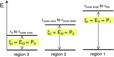 | ||
| Fig. 3 The defined energy-level spacing in three distinct regions within the nanocrystals following the potential well in Fig. 1A. | ||
In summary, according to the model of ref. 1, the origin of the suppression phenomenon is primarily related to the smooth dependence of the Zn content with radius (from rNC to r0). The potential profile is also smooth, as should be the case to effect the blinking suppression.1 Hence, the main difference in our interpretation is that we did not make this assumption. Instead, we have identified three specific regions inside the NC that lead to the observed photoluminescence. These regions with different Zn content x have different band gap values (or energy-level spacing—the cornerstone of the ionization energy approximation used), sketched in Fig. 3. These regions have been selected according to the PL measurements.1
Moreover, this “discrete-like” grading gives rise to the smooth potential profiles which change their curvature depending on the core-shell arrangements (e.g., when ZnSe is in the core or in the outer shell, see Fig. 1). This is why there is no contradiction with the most important condition (smoothness of the confining potential profile) for the blinking suppression. Apart from that, the shorter PL lifetime is most likely due to the smaller energy-level spacing as a result of grading or Zn content from one atomic layer to another. As the energy level spacing decreases, the probability of radiative recombination increases, which in turn leads to shorter photoluminescence lifetimes. This interpretation is similar to the one given in ref. 1.
6. Conclusions
In conclusion, we have considered the variation of the ionization energy or the energy-level spacing within the nanocrystals to explain the blinking effect suppression. The ionization energy theory approximation has been employed to take this energy-level spacing variation into account. By knowing the values for the atomic ionization energy EI and the band gap difference |Δ| between the core and shell in a given nanocrystal, one can predict the possibility of achieving effective non-blinking in graded NCs and/or how to switch the randomly blinking nanocrystals into a coherently emitting NCs. Moreover, by measuring the PL spectra (both intensities and the energy peaks), one can actually understand the blinking properties of the NC by studying their non-square-well potential profiles. This information can then be used to fine-tune the composition and structure of NC materials to optimize the luminescence quality and yield. In other words, one can either completely suppress the blinking effect or, alternatively, obtain highly-controlled intermittent emission. We have also presented the possibility to use the PL spectra to understand the formation of the potential well in non-blinking NCs. In addition, one can fine-tune the single and smooth potential-well by controlling the x(r) or the diffusion of Zn from the shell, ZnSe into the core, Cd1−xZnxSe. Such graded NCs can be systematically analyzed using the PL spectra that in turn could be useful to design new non-blinking NCs and non-random-blinking NCs. The potential-well profiles for the core/shell, ZnSe/Cd1−xZnxSe NCs and their relations with the emission intermittency can be straightforwardly verified experimentally. Finally, our approach is generic and can be applied to design a large variety of photon emitting devices, from single-photon emitters required for nanophotonics to high-intensity light emitting diodes, the ultimate light sources of the future.Acknowledgements
A.D.A. would like to thank Kithriammal Soosay for support. K.O. acknowledges partial support from the Australian Research Council (ARC) and the CSIRO.References
- X. Wang, X. Ren, K. Kahen, M. A. Hahn, M. Rajeswaran, S. M. Zacher, J. Silcox, G. E. Cragg, A. L. Efros and T. D. Krauss, Nature, 2009, 459, 686 CrossRef CAS.
- V. I. Klimov, A. A. Mikhailovsky, S. Xu, A. Malko, J. A. Hollingsworth, C. A. Leatherdale, H. -J. Eisler and M. G. Bawendi, Science, 2000, 290, 314 CrossRef CAS.
- R. R. Cooney, S. L. Sewall, D. M. Sagar and P. Kambhampati, Phys. Rev. Lett., 2009, 102, 127404 CrossRef.
- M. Nirmal, B. O. Dabbousi, M. G. Bawendi, J. J. Macklin, J. K. Trautman, T. D. Harris and L. E. Brus, Nature, 1996, 383, 802 CrossRef CAS.
- D. E. Gomez, J. v. Embden, J. Jasieniak, T. A. Smith and P. Mulvaney, Small, 2006, 2, 204 CrossRef CAS.
- S. Wang, C. Querner, T. Emmons, M. Drndic and C. H. Crouch, J. Phys. Chem. B, 2006, 110, 23221 CrossRef CAS.
- Ch. Rajesh, A. D. Lad, A. Ghangrekar and S. Mahamuni, Solid State Commun., 2008, 148, 435 CrossRef CAS.
- K. Dunn, J. Derr, T. Johnston, M. Chaker and F. Rosei, Phys. Rev. B: Condens. Matter Mater. Phys., 2009, 80, 035330 CrossRef.
- M. A. Green, Progr. Photovolt.: Res. Appl., 2001, 9, 137 Search PubMed.
- E. C. Cho, S. W. Park, X. Hao, D. Y. Song, G. Conibeer, S. C. Park and M. Green, Nanotechnology, 2008, 19, 245201 CrossRef.
- R. F. Service, Science, 2008, 319, 718 CrossRef CAS.
- G. Nair and M. G. Bawendi, Phys. Rev. B: Condens. Matter Mater. Phys., 2007, 76, 081304 CrossRef.
- G. Nair, S. M. Geyer, L. -Y. Chang and M. G. Bawendi, Phys. Rev. B: Condens. Matter Mater. Phys., 2008, 78, 125325 CrossRef.
- J. Derr, K. Dunn, D. Riabinina, F. Martin, M. Chaker and F. Rosei, Phys. E., 2009, 41, 668 CrossRef CAS.
- I. Sychugov, R. Juhasz, A. Galeckas, J. Valenta and J. Linnros, Opt. Mater., 2005, 27, 973 CrossRef CAS.
- M. L. Ciurea, V. Iancu and M. R. Mitroi, Solid-State Electron., 2007, 51, 1328 CrossRef CAS.
- V. Biju, T. Itoh, A. Anas, A. Sujith and M. Ishikawa, Anal. Bioanal. Chem., 2008, 391, 2469 CrossRef CAS.
- K. K. Coti, M. E. Belowich, M. Liong, M. W. Ambrogio, Y. A. Lau, H. A. Khatib, J. I. Zink, N. M. Khashab and J. F. Stoddart, Nanoscale, 2009, 1, 16 RSC.
- F. Pinaud, X. Michalet, L. A. Bentilila, J. M. Tsay, S. Doose, J. J. Li, G. Iyer and S. Weiss, Biomaterials, 2006, 27, 1679 CrossRef CAS.
- P. Sharma, S. Brown, G. Walter, S. Santra and B. Moudgil, Adv. Colloid Interface Sci., 2006, 123–126, 471 CrossRef CAS.
- J. K. Jaiswal and S. M. Simon, Trends Cell Biol., 2004, 14, 497 CrossRef CAS.
- V. Biju, Y. Makita, T. Nagase, Y. Yamaoka, H. Yokohama, Y. Baba and M. Ishikawa, J. Phys. Chem. B, 2005, 109, 14350 CrossRef CAS.
- P. H. M. Hoet, I. B. Hohfield and O. V. Salata, J. Nanobiotechnol., 2004, 2, 12 CrossRef.
- B. Sahoo, M. Goswami, S. Nag and S. Maiti, Chem. Phys. Lett., 2007, 445, 217 CrossRef CAS.
- C. Q. Sun, Prog. Solid State Chem., 2007, 35, 1 CrossRef CAS.
- A. D. Arulsamy and K. Ostrikov, J. Supercond. Novel Magn., 2009, 22, 785 Search PubMed.
- A.D. Arulsamy, Many-body Hamiltonian Based on Ionization Energy Concept: A Renormalized Theory to Study Strongly Correlated Matter and Nanostructures, PhD Thesis, The University of Sydney, 2009 Search PubMed; A. D. Arulsamy, Pramana J. Phys., 2010 Search PubMed , accepted.
- J. Wu and B. Yan, J. Alloys Compd., 2008, 455, 485 CrossRef CAS.
- T. Benbakhti, D. Mehal, S. K. Krawczyk and G. Bassou, Microelectron. J., 1999, 30, 643 CrossRef CAS.
- I. Levchenko, A. E. Rider and K. Ostrikov, Appl. Phys. Lett., 2007, 90, 193110 CrossRef.
- A. E. Rider, I. Levchenko and K. Ostrikov, J. Appl. Phys., 2007, 101, 044306 CrossRef.
- A.E. Rider, I. Levchenko and K. Ostrikov, Nanotechnology, 2008, 19, 355705 CrossRef.
- A.E. Rider and K. Ostrikov, Surf. Sci., 2009, 603, 359 CrossRef CAS.
- Q. J. Cheng, S. Y. Xu and K. Ostrikov, J. Mater. Chem., 2009, 19, 5134 RSC.
- U. Cvelbar, Z. Chen, M. K. Sunkara and M. Mozetic, Small, 2008, 4, 1610 CrossRef CAS.
- K. Ostrikov, Rev. Mod. Phys., 2005, 77, 489 CrossRef CAS.
- U. Cvelbar, K. Ostrikov, A. Drenik and M. Mozetic, Appl. Phys. Lett., 2008, 92, 133505 CrossRef.
- Q. J. Cheng, S. Xu, J. D. Long and K. Ostrikov, Appl. Phys. Lett., 2007, 90, 173112 CrossRef.
- M. J. Winter, (http://www.webelements.com), The Elements of the Periodic Table: Essential Data and Description.
- B.O. Dabbousi, J. R. Viejo, F. V. Mikulec, J. R. Heine, H. Mattoussi, R. Ober, K. F. Jensen and M. G. Bawendi, J. Phys. Chem. B, 1997, 101, 9463 CrossRef CAS.
- Y. Zhang, V. K. Komarala, C. Rodriguez and M. Xiao, Phys. Rev. B: Condens. Matter Mater. Phys., 2008, 78, 241301 CrossRef.
- J. Siegert, S. Marcinkevicius, A. Gaarder, R. Leon, S. Chaparro, S. R. Johnson, Y. Sadofyev and Y. H. Zhang, Phys. Status Solidi C, 2003, 0, 1213 Search PubMed.
- P. Spinicelli, B. Mahler, S. Buil, B. Dubertret and J.-. P. Hermier, ChemPhysChem, 2009, 10, 879 CrossRef CAS.
- E. A. Zibik, T. Grange, B. A. Carpenter, N. E. Porter, R. Ferreira, G. Bastard, D. Stehr, S. Winnerl, M. Helm, H. Y. Liu, M. S. Skolnick and L. R. Wilson, Nat. Mater., 2009, 8, 803 CrossRef CAS.
- A. D. Arulsamy, K. Ostrikov, Controlling electronic and adiabatic isolation of quantum dots from the substrate: An ionization-energy theoretic study, arXiv:0811.2631 Search PubMed.
| This journal is © The Royal Society of Chemistry 2010 |