A dithienyl benzotriazole-based poly(2,7-carbazole) for field-effect transistors and efficient light-emitting diodes
Bo
Liu
ab,
Yingping
Zou
*bd,
Shanghui
Ye
c,
Yuehui
He
*a and
Kechao
Zhou
a
aState key Laboratory for Powder Metallurgy, Central South University, Changsha, 410083, China
bCollege of Chemistry and Chemical Engineering, Central South University, Changsha, 410083, China. E-mail: yingpingzou@csu.edu.cn
cJiangsu Key Laboratory of Organic Electronics and Information Displays and Institute of Advanced Materials (IAM), Nanjing University of Posts & Telecommunications (NUPT), Nanjing, 210046, China
dState Key Laboratory of Optoelectronic Materials and Technologies, Sun Yat-sen Unversity, Guangzhou, 510275, China
First published on 10th August 2011
Abstract
In this work, a donor–acceptor type copolymer, poly[(N-9′-heptadecanyl-2,7-carbazole)-alt-(4,7-bis(2′-thienyl)-2-dodecyl-2,1,3-benzotriazole)] (PCDTBTz) is introduced for versatile applications in organic electronics. PCDTBTz exhibits excellent solubility, film-forming ability and morphological stability, along with charming optoelectronic properties. The solution processable OFET device displays typical p-type transporting characteristics with a moderate mobility up to 4.3 × 10⁻⁴ cm2/V·s upon thermal annealing at 80 °C, and PLEDs in the device structure of ITO/PEDOT:PSS (10 nm)/Poly-TPD (30 nm)/PCDTBTz (32 nm)/Alq3 (40 nm)/Ca:Ag show a bright orange red emission with a maximum brightness of 13![[thin space (1/6-em)]](https://www.rsc.org/images/entities/char_2009.gif) 655 cd/m2 at 1607.9 mA/cm2 and 12.6 V, and a maximum EL efficiency of 0.85 cd/A. All the results indicate that PCDTBTz is a promising candidate for optoelectronic materials used in both for polymer FETs and LEDs.
655 cd/m2 at 1607.9 mA/cm2 and 12.6 V, and a maximum EL efficiency of 0.85 cd/A. All the results indicate that PCDTBTz is a promising candidate for optoelectronic materials used in both for polymer FETs and LEDs.
Introduction
Conjugated polymers have gained great attention since the discovery of conducting polyacetylene in 1977. Among the conjugated polymers, poly(2,7-carbazole)s have emerged as promising conjugated polymers for plastic electronics since their first synthesis by the Leclerc group in 2001.1 Excellent ambient and chemical stability (i.e., low HOMO energy levels), good p-type charge transport and easy modulation of the optic-physical properties made poly(2,7-carbazole) derivatives excellent candidates in polymer solar cells,2,3 light-emitting diodes,4,5 electrochromism devices6 and field-effect transistors (FETs).7 In order to improve the optoelectronic properties to meet the requirements for different applications, chemical modifications of poly(2, 7-carbazole)s have been well performed.Organic field effect transistors (OFETs) have attracted great interests because of their promising applications in organic sensors,8 integrated circuit, low-cost large area memories, smart cards, and driving circuits for large-area displays.9,10 One of the most important aspects for OFETs is that they can be fabricated by easy patterning techniques at low cost and have good compatibility with flexible plastic substrates. Thus, solution processable polymers are preferable to small molecules. Design and synthesis of new conjugated polymer semiconductors with high mobility is highly desirable for the realization of high-performance solution processable OFETs.
During the process of developing plastic electronics, polymer light emitting diodes (PLEDs) also stimulated broad attractions from academic and industrial circles due to their large fabrication area, low power consumption, wide viewing angle, good contrast and video rate operation.11 Although much effort has been devoted to this, up to date, the excellent electroluminescent polymers are still limited. Therefore, the design and synthesis of new conjugated polymers for high performance LEDs are of great interest.12
An important feature of conjugated polymers lies in the versatility of their molecular structure which provides flexibility to construct new polymers with improved properties. Benzotriazole (BTz) is a known heteroaromatic compound with a strong electron accepting feature because of two electron withdrawing imine (C![[double bond, length as m-dash]](https://www.rsc.org/images/entities/char_e001.gif) N) nitrogens, furthermore, the easy modification of the N–H bond of the BTz unit is beneficial for the construction of a conjugated polymer with better solubility. The good solubility of a conjugated polymer is important for its purification and the formation of high-quality films for efficient optoelectronic devices. Polymers containing BTz or its derivatives possess unique optoelectronic properties for diverse applications such as light emitting diodes, photovoltaic devices and electrochromic devices. For example, Yamamoto and coworkers reported the synthesis and optical properties of BTz-containing homopolymers and copolymers.13 Cao et al. synthesized the copolymers from fluorene and BTz units, emitting blue electroluminescence.14 Gong and Cao et al. copolymerized BTz segment with phenothiazine vinylene units to obtain orange-red light emitting copolymers.15 Recently, Toppare et al. copolymerized BTz units with 3,4-ethylenedioxythiophene segments to construct some copolymers which showed enhanced electrochromic properties compared to PEDOT.16a Following this work, the same group obtained the copolymer from BTz units and thiophene comonomers, which exhibited some interesting electrochromic properties.16b Recently, BTz-based or dithienyl benzotriazole (DTBTz)-based photovoltaic copolymers with PCEs above 2% after device modification have been demonstrated by Chen's group17a and You's group.17b However, BTz or DTBTz based copolymers behaving as both electroluminescent and FET materials remain still unexplored. Therefore, it is necessary for us to further investigate the potential of DTBTz based polymers.
N) nitrogens, furthermore, the easy modification of the N–H bond of the BTz unit is beneficial for the construction of a conjugated polymer with better solubility. The good solubility of a conjugated polymer is important for its purification and the formation of high-quality films for efficient optoelectronic devices. Polymers containing BTz or its derivatives possess unique optoelectronic properties for diverse applications such as light emitting diodes, photovoltaic devices and electrochromic devices. For example, Yamamoto and coworkers reported the synthesis and optical properties of BTz-containing homopolymers and copolymers.13 Cao et al. synthesized the copolymers from fluorene and BTz units, emitting blue electroluminescence.14 Gong and Cao et al. copolymerized BTz segment with phenothiazine vinylene units to obtain orange-red light emitting copolymers.15 Recently, Toppare et al. copolymerized BTz units with 3,4-ethylenedioxythiophene segments to construct some copolymers which showed enhanced electrochromic properties compared to PEDOT.16a Following this work, the same group obtained the copolymer from BTz units and thiophene comonomers, which exhibited some interesting electrochromic properties.16b Recently, BTz-based or dithienyl benzotriazole (DTBTz)-based photovoltaic copolymers with PCEs above 2% after device modification have been demonstrated by Chen's group17a and You's group.17b However, BTz or DTBTz based copolymers behaving as both electroluminescent and FET materials remain still unexplored. Therefore, it is necessary for us to further investigate the potential of DTBTz based polymers.
Based on these considerations, our group recently synthesized a DTBTz based polymer, PCDTBTz, for photovoltaic applications, this polymer exhibited moderate photovoltaic performance with a PCE up to 2.2%.18 Following this work, herein, we report the electroluminescent and FET properties of PCDTBTz. The investigations show that the polymer possesses good mobility with high switch ratio, furthermore, the polymer exhibits excellent electroluminescent properties with a maximum brightness of 130![[thin space (1/6-em)]](https://www.rsc.org/images/entities/char_2009.gif) 655 cd/m2 and a current efficiency of 0.85 cd/A. All the results show that this polymer (PCDTBTz) is a promising candidate as a multi-purpose material in versatile applications in polymer solar cells, electroluminescent devices and field effect transistors.
655 cd/m2 and a current efficiency of 0.85 cd/A. All the results show that this polymer (PCDTBTz) is a promising candidate as a multi-purpose material in versatile applications in polymer solar cells, electroluminescent devices and field effect transistors.
Experimental
Materials
Pd(PPh3)4, thiophene-2-boronic acid and PPh3 were obtained from Pacific Chemical Source Co, and they were used as received without further purification. Tetrahydrofuran (THF) was dried over Na/benzophenone ketyl and freshly distilled prior to use. Other reagents and solvents were purchased commercially as analytical-grade quality and used without further purification. PCDTBTz was synthesized according to our previous work.18Fabrication of FET devices
Thin-film FETs were fabricated with top-contact configuration. An n-doped Si wafer with a thermally grown silicon dioxide layer (thickness of 450 nm) was used as the substrate. The substrates were cleaned in water, alcohol, acetone, and rinsed in deionized water. Thin polymer films were prepared by spin coating of a 0.3 wt% solution of PCDTBTz in chloroform onto the bare SiO2/Si substrates at a speed of 3000 rpm (revolutions per minute) for 40 s at room temperature. After drying at 80 °C under N2 for half an hour, a gold film (50 nm) was deposited on the organic layer to form the drain and source electrodes, for a typical device, the drain-source channel length (L) and width (W) are 50 μm and 3000 μm, respectively. FET measurements were performed at room temperature using a Keithley 4200SC semiconductor parameter analyzer under ambient conditions. AFM images were obtained using a Veeco's Dimension V atomic force microscopic (AFM) in tapping mode.Fabrication of PLED devices
In a general procedure, indium-tin oxide (ITO)-coated glass substrates were etched, patterned, and washed with detergent, deionized water, acetone, and ethanol in turn. A thin layer of Poly-TPD serving as a hole-transporting layer was spin-coated from toluene solution on the PEDOT:PSS smoothed ITO surface, on which the emitting-layer of PCDTBTz was cast from chlorobenzene solution and annealed at 80 °C for 30 min. After that it was transferred to a vacuum chamber where a thin layer of tris(8-hydroxyquinoline)aluminum, Alq3, and calcium was deposited to enhance electron-injection and transporting ability, respectively, at a pressure of 8 × 10⁻⁵ Pa. In all devices, a 100 nm thick of Ag capping layer was deposited through a 2 mm diameter opening in a shadow mask. The active area of the device was 5 mm2. A quartz crystal oscillator near the substrate was used to monitor the thickness of each layer, which was calibrated ex situ using an Ambios Technology XP-2 surface profilometer. EL spectra and chromaticity coordinates were measured with a Spectra-Scan PR650 photometer. Current density-voltage-luminance (J-V-L) measurements were conducted simultaneously using a Keithley 4200 semiconductor parameter analyzer and a Newport multifunctional 2835-C optical meter, with luminance measured in the forward direction.Results and discussion
Organic field effect transistors
FETs based on PCDTBTz were fabricated using solution processing. The FETs of PCDTBTz exhibited typical p-channel OFET characteristics.In the FETs, drain current (IDS) can be described with the following equation:
Where Ci is the capacitance per unit area of the gate dielectric layer, VG is the gate voltage, VT is the threshold voltage, μ is the field-effect mobility, and W and L are the channel width and length dimensions, respectively. The mobility was calculated from the slope of the curve of IDS1/2vs. VG. The threshold voltage of the device was determined from the linear fit of the square root of IDS at the saturated regime vs. gate voltage VG, and VT was determined by extrapolating the measured data to IDS = 0.
Fig. 1a shows the transfer characteristic of PCDTBTz without thermal annealing. In this case, the hole mobility was 2.7 × 10⁻⁴ cm2/V·s with the on/off ratio of 104. Fig. 1b shows the transfer characteristic of PCDTBTz after annealing at 80 °C, the hole mobility increased up to 4.3 × 10⁻⁴ cm2/V·s. After annealing, the hole mobility was higher than that without thermal annealing, because the thermal annealing increases the surface smoothness of PCDTBTz thin films as shown in Fig. 2. As-spun films of PCDTBTz are always rougher than those of annealed thin films, independent of substrate chemistry. The morphology of the films is in agreement with their trend of charge transport performances. The hole mobility was increased upon annealing at 80 °C and it was apparently correlated with the surface morphology, indicating a strong relationship between morphology and device performances (Table 1).
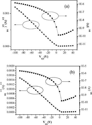 | ||
| Fig. 1 Transfer characteristics of PCDTBTz thin films, (a) without thermal annealing; (b) annealing at 80 °C. | ||
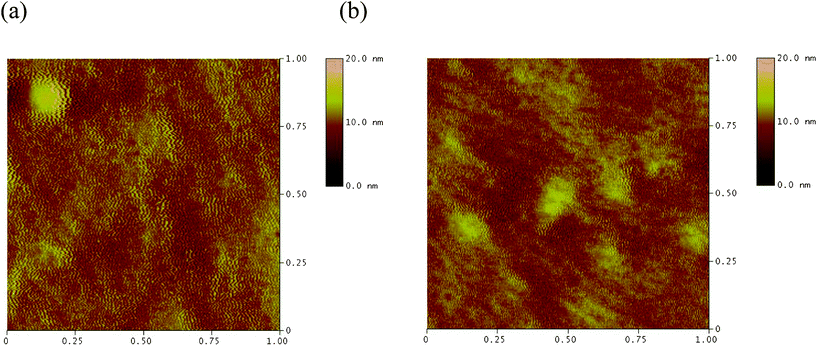 | ||
| Fig. 2 AFM images of PCDTBTz thin films: (a) without thermal annealing; (b) annealed at 80 °C. | ||
| Temperature | Rs (nm) | Ra (nm) | Rmax (nm) |
|---|---|---|---|
| a The root mean square roughness, Rs, is essentially the standard deviation of the asperity heights above and below the data. The image mean roughness, Ra, is the arithmetic average of the absolute values of the surface height deviations measured from the mean plane. The maximum height roughness, Rmax, is the difference in height between the highest and lowest points on the surface relative to the mean plane. | |||
| 25 °C | 2.153 | 1.331 | 9.183 |
| 80 °C | 1.582 | 1.085 | 6.488 |
Electroluminescent properties
As a multifunctional material, our synthesized polymer not only exhibited excellent film-forming and morphological stability, suitable hole mobility, but also electroluminescent properties. To testify our assumption, we made polymer LEDs by utilizing our synthesized polymer as emitting-layer coupled with Poly-TPD hole-transporting layer and Alq3 electron-transporting layer in a simple sandwich structure. Due to the good solubility and film-forming ability of this polymer, we explored a solution processable method to fabricate devices. The fabricated device configuration is ITO/PEDOT:PSS (10 nm)/Poly-TPD (30 nm)/PCDTBTz (32 nm)/Alq3 (40 nm)/Ca:Ag. We chose Poly-TPD as the hole-transporting layer (HTL) because of its good solvent resistance ability as well as suitable energy level to facilitate the hole transport from the ITO anode to the EML.Fig. 3 shows the electroluminescent (EL) spectra of the devices under various voltages. Compared to that of PL,18 the EL spectrum of PCDTBTz exhibited a similar emission, which indicates that the same excitation mechanisms were involved in both cases. All the devices showed a bright orange red emission when an appropriate forward bias was applied. The maximum emission peak of PCDTBTz was observed at 595 nm, accompanied by a shoulder peak at 565 nm, and remained very stable against the applied voltage in the range of 5 V to 8 V. As the applied voltage increased, the EL intensity of the polymer increased. And the Commission of Internationale de L'Eclairage coordinates x, y (CIEx,y) remained stable with very slight deviation. For example, the CIEx,y were (0.549, 0.450) at 5 V, and drifted to (0.543, 0.455) and (0.538, 0.460) at 6 V and 8 V, respectively.
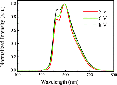 | ||
| Fig. 3 EL spectrum of the PCDTBTz device. | ||
As expected, our device exhibited a bright orange red emission with the maximum brightness of 13 655 cd/m2 at 12.6 V, for details see Table 2. The turn-on voltage at a brightness of 1 cd/m2, was recorded at 2.8 V, which is relatively low. The current density increases exponentially with the increasing forward voltage, which was a typical diode characteristics, as shown in Fig. 4. The maximum current density reached 1607.9 mA/cm2 at 12.6 V and the corresponding brightness reached the maximum value. High brightness accompanied by high current density means that our PCDTBTz is a good emitter.
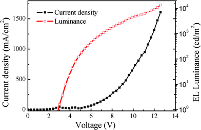 | ||
| Fig. 4 Current density-Luminance-Voltage (J-L-V) characteristics of the PCDTBTz device. | ||
| Light-emitting layer | LE a [cd A−1] | PE a [lm W−1] | CIE b [x, y] | LE b [cd A−1] | PE b [lm W−1] | LE c [cd A−1] | PE c [lm W−1] | Lmax [cd m−2]d |
|---|---|---|---|---|---|---|---|---|
| a Maximum efficiency. b Values recorded at a luminance of 100 cd m−2. c Values recorded at 1000 cd m−2. d The data in the parentheses are the corresponding current density. | ||||||||
| PCDTBTz | 0.85 | 0.37 | 0.549, 0.450 | 0.55 | 0.36 | 0.68 | 0.30 | 13654.7/1607.9 |
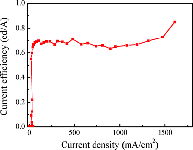
Fig. 5 shows the current efficiency-current density characteristic of the device with the maximum current efficiency of 0.85 cd/A at around 1600 mA/cm2. A sharp feature of the efficiency-density characteristic is that the current efficiency remained stable and even a little increased upon current density increase, which is rare in the literature. For example, the EL efficiency reached 0.70 cd/A at 100 mA/cm2, and increased to 0.71 cd/A at 500 mA/cm2, and pumped to 0.75 cd/A at 1500 mA/cm2, for details see Table 2. Another thing worth mentioning is that the maximum efficiency was reached at a more practical current density of around 500–2000 mA/cm2 and maintained very stable against the current density's increase, which means it is more useful for commercial application.19 These results indicate that PCDTBTz is an excellent orange red electroluminescent material.
 | ||
| Fig. 5 Current efficiency-Current density characteristics of the PCDTBTz device. | ||
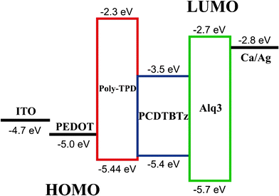
For a given emitting material, device structure is a decisive factor in the EL efficiency. Fig. 6 shows the schematic energy level diagram of the device and the corresponding HOMO/LUMO energy level of the materials used.18 The injection barrier for both hole and electron are relative small, within 0.1 eV, which suggests that carriers and excitons were well confined in the EML while the electron and hole confining barrier at the interface of Poly-TPD/EML and EML/Alq3 is 1.2 eV and 0.8 eV, respectively. Thus the low EL efficiency of the device may be due to the imbalanced holes and electrons injection and transportation in the EML layer. As demonstrated in the literature the Alq3 has an electron mobility in the range of 10−5 ∼ 10−6 cm2/V·s,20 while our synthesized polymer is a hole-type emitter with hole mobility of 2.7 × 10⁻⁴ ∼ 4.3 × 10⁻⁴ cm2/V·s, and thus hole accumulation in the EML/Alq3 interface can be imagined. Further improvement in the EL efficiency may be achieved by searching for high mobility electron-type materials to replace Alq3.
 | ||
| Fig. 6 Schematic energy level diagram of the PCDTBTz device. | ||
Conclusions
In summary, we have introduced a multi-purpose polymer PCDTBTz for OFET and PLED. This polymer showed excellent solubility, film-forming ability and morphological stability, making solution processable optoelectronic devices possible. Solution processable OFET devices exhibit p-type transporting characteristics with a moderate mobility up to 4.3 × 10⁻⁴ cm2/V·s after thermal annealing, and PLEDs displayed a bright orange red emission with maximum brightness of 13 655 cd/m2 at 1607.9 mA/cm2 and 12.6 V, and maximum EL efficiency of 0.85 cd/A. High brightness accompanied by high current density suggests our synthesized polymer is a good emitter. All the results indicate that PCDTBTz is a promising candidate both for polymer FETs and LEDs.Acknowledgements
The authors acknowledge Zhenhua Zhang for the synthesis of the intermediates. This work was supported by Lieying Project, the Fundamental Research Funds for the Central Universities (2010QZZD0112), Doctoral Fund of Ministry of Education of China (20100162120033), the Open Fund of the State Key Laboratory of Optoelectronic Materials and Technologies (Sun Yat-sen Unversity)(KF2010-MS-01).References
- J.F. Morin and M. Leclerc, Macromolecules, 2001, 34, 4680 CrossRef CAS.
- R. Qin, W. Li, C. Li, C. Du, C. Veit, H. Schleiermacher, M. Andersson, Z. Bo, Z. Liu, O. Inganäs, U. Wuerfel and F. Zhang, J. Am. Chem. Soc., 2009, 131, 14612 CrossRef CAS.
- Y. Zou, D. Gendron, R. B.Aich, A. Najari, Y. Tao and M. Leclerc, Macromolecules, 2009, 42, 2891 CrossRef CAS.
- J. F. Morin, S. Beaupre, M. Leclerc, I. Levesque and M. D'Iorio, Appl. Phys. Lett., 2002, 80(3), 341 CrossRef CAS.
- R. S. Liu, W. J. Zeng, B. Du, W. Yang, Q. Hou, W. Shi, Y. Zhang and Y. Cao, Chin. J. Polym. Sci., 2008, 26, 231 CrossRef CAS.
- S. Beaupré, A. C. Breton, J. Dumas and M. Leclerc, Chem. Mater., 2009, 21, 1504 CrossRef.
- S. Wakim, N. Blouin, E. Gingras, Y. Tao and M. Leclerc, Macromol. Rapid Commun., 2007, 28, 1798 CrossRef CAS.
- H. U. Khan, M. E. Roberts, O. Johnson, R. Förch, W. Knoll and Z. Bao, J. Mat. Chem. Search PubMed DOI: 10.1021/cm103685c.
- G. B. Blanchet, Y. Loo, J. A. Rogers, F. Gao and C. R. Fincher, Appl. Phys. Lett., 2003, 82, 463 CrossRef CAS.
- Y. Qiu, Y. Hu, G. Dong, L. Wang, J. Xie and Y. Ma, Appl. Phys. Lett., 2003, 83, 1644 CrossRef CAS.
- D. H. Hwang, S. K. Kim, M. J. Park, J. H. Lee, B. W. Koo, I. N. Kang, S. H. Kim and T. Zyung, Chem. Mater., 2004, 16, 1298 CrossRef CAS.
- M. T. Bernius, M. Inbasekaran, J. O'Brien and W. Wu, Adv. Mater., 2000, 12, 1737 CrossRef CAS.
- A. Tanimoto and T. Yamamoto, Macromolecules, 2006, 39, 3546 CrossRef CAS.
- M.L. Sun, Q.L. Niu, R.Q. Yang, B. Du, R.S. Liu, W. Yang, J.B. Peng and Y. Cao, Eur. Polym. J., 2007, 43, 1916 CrossRef CAS.
- Y. L. Liu, H. Y. Cao, J. H. Li, Z. J. Chen, S. K. Cao, L. X. Xiao, S. G. Xu and Q. H. Gong, J. Polym. Sci., Part A: Polym. Chem., 2007, 45, 4867 CrossRef CAS.
- (a) A. Balan, D. Baran, G. Gunbas, A. Durmus and L. Toppare, Chem. Mater., 2008, 20, 7510 CrossRef CAS; (b) A. Balan, D. Baran, G. Gunbas, A. Durmus, F. Ozyurt and L. Toppare, Chem. Commun., 2009, 44, 6768 RSC.
- (a) L. Zhang, C. He, J. Chen, P. Yuan, L. Huang, C. Zhang, W. Cai, Z. Liu and Y. Cao, Macromolecules, 2010, 43, 9771 CrossRef CAS; (b) S.C. Price, A.C. Stuart, L. Yang, H. Zhou and W. You, J. Am. Chem. Soc., 2011, 133, 4625 CrossRef CAS.
- B. Peng, A. Najari, B. Liu, P. Berrouard, D. Gendron, Y. H. He, K. C. Zhou, Y. P. Zou and M. Leclerc, Macromol. Chem. Phys., 2010, 211, 2026 CrossRef CAS.
- P. I. Shih, C. Y. Chuang, C. H. Chien, E. W. G. Diau and C. F. Shu, Adv. Funct. Mater., 2007, 17, 3141 CrossRef CAS.
- (a) S. Barth, P. Müller, H. Riel, P. F. Seildler, W. Riess, H. Vestweber and H. Bässler, J. Appl. Phys., 2001, 89, 3711 CrossRef CAS; (b) S.J. Su, T. Chiba, T. Takeda and J. Kido, Adv. Mater., 2008, 20, 2125 CrossRef CAS.
| This journal is © The Royal Society of Chemistry 2011 |


