X-ray photoelectron spectroscopy study of lithium thio-germanate thin films†
Inseok
Seo
and
Steve W.
Martin
*
Department of Materials Science and Engineering, Iowa State University, 2220 Hoover Hall, Ames, Iowa 50011, USA. E-mail: swmartin@iastate.edu; Fax: (515) 294-5444; Tel: (515) 294-0745
First published on 16th August 2011
Abstract
In this study, the compositions of and chemical speciation in lithium thio-germanate thin films grown by radio frequency (RF) magnetron sputtering were determined by means of X-ray photoelectron spectroscopy (XPS). Three different targets, nLi2S + GeS2 (n = 1, 2, and 3) for RF sputtering were prepared. Thin films of ∼1 μm thickness were grown on single crystal Si [111] substrates using 50 W power and ∼3.3 Pa Ar gas atmospheres. As is commonly observed for RF sputtered non-oxide films, the surfaces of these lithium thio-germanate films were contaminated with both C and O at ∼10 at %. Etching the top surface of the films with Ar removed all of the surface carbon and reduced the oxygen contamination down to an average value of ∼5 at %. After such surface etching, the compositions of the films were found to agree very closely with the nominal composition of the target from which it was made. The Li2GeS3 (n = 1) thin film was found as expected to exhibit a 2![[thin space (1/6-em)]](https://www.rsc.org/images/entities/char_2009.gif) :1 non-bridging sulfur (
:1 non-bridging sulfur (![[triple bond, length as m-dash]](https://www.rsc.org/images/entities/char_e002.gif) Ge–S−Li+, NBS) to bridging sulfur (Ge–S–Ge, BS) ratio. As the Li2S content increased, the Li4GeS4 and Li6GeS5 thin films, n = 2 and 3, exhibited as expected, 100% NBS. For the S2p core peaks, the binding energy of S in GeS2 is the highest due to the nearly covalent bonding in the BS structure, Ge–S–Ge. As the Li2S content increased, the binding energy of S in the thin films progressively decreased due to the progressive increase in the fraction (and number) of NBS (more ionic), Ge–S−Li+, in the films.
Ge–S−Li+, NBS) to bridging sulfur (Ge–S–Ge, BS) ratio. As the Li2S content increased, the Li4GeS4 and Li6GeS5 thin films, n = 2 and 3, exhibited as expected, 100% NBS. For the S2p core peaks, the binding energy of S in GeS2 is the highest due to the nearly covalent bonding in the BS structure, Ge–S–Ge. As the Li2S content increased, the binding energy of S in the thin films progressively decreased due to the progressive increase in the fraction (and number) of NBS (more ionic), Ge–S−Li+, in the films.
Introduction
Renewable energy harvesting, conversion, storage, and distribution are of great interest due to the demand created by portable electronics and transportation.1–3Lithium-based batteries have begun to meet these demands due to the high energy densities of lithium-carbon anodes. However, the theoretical energy capacity of lithium metal is ∼10 times higher than that of lithium-carbon anodes at ∼3860 mAh g−1vs. ∼372 mAh g−1.4 Recently, lithium based thin film batteries have been of interest in miniaturized power electronics such as smart cards.5 In addition, thin film batteries are candidates for high power applications such as electric/hybrid vehicles.6 Thin film batteries show smaller temperature dependences and are able to address the safety issues of aqueous flammable electrolytes.7So far, lithium phosphorous oxy-nitride (LiPON) thin film electrolytes are the most commonly used because LiPON shows good chemical and electrochemical stability in contact with metallic lithium, high cyclability, and facile fabrication.8–9 However, this easily prepared and chemically stable solid electrolyte has a relatively low Li+ ion conductivity of ∼10−6 (S cm−1) at 25 °C compared to sulfide materials which have Li+ ion conductivities in the range of ∼10−3 to ∼10−4 (S cm−1) at 25 °C.10–16
For these reasons, sulfide materials have attracted attention for electrochemical applications. While many reports have been made of bulk sulfide glasses,17–21 there are very few reports of sulfide thin films because of the difficulty in preparing them.22–23 Furthermore, of the few reports that do exist on sulfide thin films in the open literature, most show that the films tended to be strongly oxidized either during sputtering, caused possibly by leakage of the RF chamber, or by exposure to air after sputtering.23 In addition, these thin films were found to be Li deficient compared to that of the targets from which they were made.23 Therefore, although sulfide films may have good potential in thin film batteries, the sulfide thin films produced so far appear to be less than optimized and for this reason have found limited applications.
In order to investigate sulfide-based thin films more extensively, in this study lithium thio-germanate thin films were carefully sputtered under well controlled conditions and then carefully analyzed by X-ray photoelectron spectroscopy (XPS). XPS is one of the best methods to determine the composition of thin film materials, even of light elements such as lithium, and it is also effective in investigating the characteristics (valence) of the constituent atoms (ions) in the thin films by monitoring their binding energies. To minimize contamination of the films produced in this work, every experimental step was performed carefully and in particular, the RF sputtering conditions were optimized to obtain consistency between target and thin film compositions and to specifically produce films with near stoichiometric lithium concentrations. The starting materials, Li2S and GeS2, the target materials, and thin films were characterized by XPS for compositional and chemical shift analysis.
Results and discussion
Analysis of the Li2S and GeS2 starting materials
In order to verify the purity of the starting materials, the Li2S and GeS2 were examined by XPS. In the case of the commercially purchased Li2S material, Table 1 shows that the concentration of C and O were ∼12% and ∼21% (±3%), respectively, and as such are relatively high. One possibility is that the Li2S was slightly contaminated on the surface in the glovebox because the glovebox contained several ppm level of oxygen. Another possible reason for this can also include the “see-through” effect due to the double-sided tape used to adhere the powder to the XPS sample holder.| At% | Li1s | Ge2p3 | S2p | C1s | O1s | Comments |
|---|---|---|---|---|---|---|
| Li2S | 44.7 | — | 22.9 | 11.7 | 20.7 | As-prepared |
| 66.1 | — | 33.9 | — | — | Ignore C and O | |
| 66.7 | — | 33.3 | 0.0 | 0.0 | Expected values | |
| GeS2 | — | 34.2 | 59.2 | 6.6 | 0.0 | As-prepared |
| — | 35.7 | 64.3 | — | 0.0 | Ignore C | |
| — | 33.3 | 66.7 | 0.0 | 0.0 | Expected values |
The ratio of Li to S, however, 1.95:1.00 is very close to the expected value of 2:1. From Table 1, while the Li2S shows relatively high O content, the GeS2 material was not contaminated by oxygen due in part to the fact that GeS2 material is less hygroscopic than other sulfide materials, but also due to the fact that this material was prepared from high purity starting materials, Ge and S (99.9999%), in the very controlled conditions of our laboratory. GeS2 contains a small percent of C, presumably surface C, see Table 1, and after ignoring C, the compositional data of GeS2 agrees well with expected values.
Deconvoluted S2p core XPS spectra for crystalline Li2S (a) and glassy GeS2 (b) starting materials are shown in Fig. 1. The binding energies for sulfur in Li2S and GeS2 are at 160.7 eV and 163.2 eV ±0.2 eV, respectively. The reason for the difference in the S2p binding energies between Li2S and GeS2 is that S in Li2S is the fully ionic S2−sulfide anion and the S in the GeS2 is the fully covalent BS, Ge–S–Ge, and hence the binding energy of the covalent BS is higher than that of the ionic sulfide. For the S2p spectra of sulfur species, there is a doublet consisting of S2p3/2 and S2p1/2 spin–orbit coupled electrons in the intensity ratio of 2:1. The S2p core peaks of Li2S show one doublet. This doublet arises from the Li2S bonding and means that only the Li2S bonding exists. This result agrees well with the literature data.24 If Li2S was significantly contaminated by oxygen, the deconvoluted S2p spectra would be expected to show additional peaks related to sulfite SO32− (166 eV) and/or sulfate SO42− (172 eV) contamination25. Both the Li2S and GeS2 materials do not show significant peaks at 166 eV and 172 eV and suggests that these materials are of high purity. The deconvoluted S2p core peaks of the GeS2 also show, as expected, only one doublet arising from the single bridging sulfur structure, Ge–S–Ge.
 | ||
| Fig. 1 Deconvoluted S2p core XPS spectra for Li2S (a) and GeS2 (b). | ||
Target material analysis
After the target materials for the RF sputtering were made using nLi2S + GeS2, n = 1, 2 and 3, their compositions were determined by XPS. The compositional data of the three target materials are shown in Table 2. The target materials show C and O contents and therefore the Li, Ge and S contents are lower than the expected values. If C and O elements are ignored, the compositional data of Li, Ge and S for all three target materials nearly match with the expected values. Although the XPS compositional data are different between the collected and expected data, the differences are within the confidence error limit, ±3%. Considering the ±3% error of the XPS data, the small Li deficiency can be ignored.| At% | Li1s | Ge2p3 | S2p | C1s | O1s | Comments |
|---|---|---|---|---|---|---|
| Li2GeS3 target | 26.1 | 16.4 | 41.3 | 10.3 | 5.9 | As-prepared |
| 30.4 | 19.1 | 48.1 | — | — | Ignore C and O | |
| 33.3 | 16.7 | 50.0 | 0.0 | 0.0 | Expected values | |
| Li4GeS4 Target | 36.5 | 9.6 | 40.2 | 8.6 | 5.1 | As-prepared |
| 42.3 | 11.1 | 46.6 | — | — | Ignore C and O | |
| 44.4 | 11.2 | 44.4 | 0.0 | 0.0 | Expected values | |
| Li6GeS5 target | 40.4 | 8.0 | 37.2 | 6.5 | 7.9 | As-prepared |
| 47.2 | 9.3 | 43.5 | — | — | Ignore C and O | |
| 50.0 | 8.3 | 41.7 | 0.0 | 0.0 | Expected values |
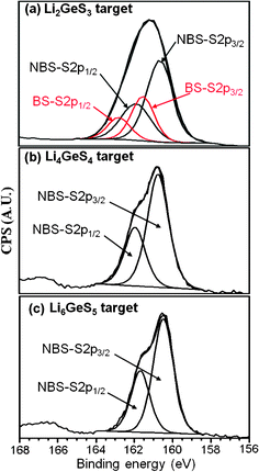
Ar etching treatments were not performed to remove surface C and O because the target materials were in the form of powders and Ar etching does not work well for powders that do not have large flat smooth surfaces. The deconvoluted S2p spectra of the three target materials are shown in Fig. 2. From the spectra in Fig. 2, the binding energies of the NBS, Ge–S−Li+ and BS, Ge–S–Ge can be obtained. By comparing these XPS spectra to that of the standard materials, it can be determined that the sulfur spectra do not contain peaks related to sulfite SO32− or sulfate SO42− anions which would be shifted to significantly higher binding energies due to their S+4 and S+6oxidation states, respectively. This suggests that although the target materials show some oxygen content as shown in Table 2, the contamination may only be on the surface. The low oxygen content is associated with the high purity of the starting materials as well as the fact that the target materials were made in a N2 filled high quality glovebox. As shown in Fig. 2, while two doublets appear in the deconvoluted S2p core peaks of the Li2GeS3 target material indicating that there are two chemically distinct surface species, the Li4GeS4 and Li6GeS5 targets show only one doublet indicating a single chemical species for sulfur.
 | ||
| Fig. 2 Deconvoluted S2p core XPS spectra of the Li2GeS3 (a), Li4GeS4 (b), and Li6GeS5 (c). | ||
The binding energies of sulfur in the target compositions and the NBS and BS ratios of the three target materials are shown in Table 3. In order to compare the chemical shifts, the binding energies of the GeS2 and Li2S are also listed in Table 3. While the binding energy of S in GeS2 shows the highest value due to its BS structure, the binding energy of S in Li2S shows the lowest value. The binding energies of the target materials are similar to one another and, as expected, are between that of GeS2 and Li2S. In the S XPS spectrum of the Li2GeS3 target, the low energy doublet is assigned to the NBS and the other higher energy doublet is assigned to the BS. For the Li2GeS3 target material, the ratio of the NBS and BS is 65.3% to 34.7%. The expected ratio of NBS to BS in the Li2GeS3 target composition agrees well with that calculated from the composition of 67% to 33%.26 Theoretically, the ratio of the NBS and BS in the Li4GeS4 target should be 100% and 0%, respectively. As shown in Table 3, the Li4GeS4 target material shows 100% NBS and 0% BS ratio. Additionally and as expected, the Li6GeS5 target material shows 100% NBS and 0% BS.
As described above, Li2S consists of only the S= anion whereas Li4GeS4 consists of 100% NBS. From the composition, it is expected that the Li6GeS5 target should be composed of an equimolar mixture of Li2S and Li4GeS4. However, the XPS spectra data shown in Table 3 shows that Li6GeS5 consists of only 100% NBS and 0% BS. Strictly speaking, Li6GeS5 should consist of Li4GeS4 which has 100% NBS and Li2S which has 100% ionic sulfur, S2−. While the binding energies of the S2− anion and the NBS are very close, the resolution of our XPS instrument appears to be insufficient to differentiate the chemical shift of S2− anion and the NBS unit, Ge–S−Li+.
The structure of Li2GeS3, Li4GeS4 and Li6GeS5 targets consist of the progressive addition of Li2S to GeS2 to create increasing amounts of NBS which replace the BS. The chemical short range structures of GeS2, Li2GeS3, Li4GeS4, and Li6GeS5 are shown in Fig. 3 which shows that the fraction of NBS to BS progressively changes from 0:2, 2:1, 4:0, and 4:0 across this series. The latter composition, Li6GeS5, would be expected to consist of equimolar amounts of Li2S and Li4GeS4.
 | ||
| Fig. 3 The schematic structures of GeS2, Li2GeS3, Li4GeS4, and Li6GeS5. | ||
Compositional analysis of the lithium thio-germanate thin films
After sputtering thin films on Ni coated Si substrates in Ar atmospheres, they were characterized by XPS to determine their compositions and chemical shifts. It was found that a Ni protective layer on the Si was necessary to prevent reaction of the Si with the Li which produces highly Li deficient films. This is described below in the experimental section. The compositional data of all of the thin films sputtered in Ar atmospheres using the three different targets are shown in Table 4. For the as-prepared thin films, the C and O contents are slightly higher than those of the targets and the Li, Ge and S contents are slightly lower than their expected values. It is assumed that this arises due to the intrinsically higher chemical reactivity of the surface of thin films compared to bulk materials. In order to obtain more accurate compositional data of the thin films, Ar etching was performed on the thin film surfaces for 1 min and 5 min at a rate of ∼1 nm min−1. As shown in Table 4, after Ar etching for 1 min. the C content in the thin films reduced to 0% and the O content decreased significantly. Although some O content still exists in the thin films, the Li, Ge, and S contents in the thin films are very close to their expected values. In order to examine deeper profiles of the thin film, Ar etching for 5 min. was performed at ∼1 nm min−1etching rate. After Ar etching for 5 min was performed, the compositional data are almost the same compared to the data obtained after Ar etching for 1 min. This suggests that the thin films show high uniformity and quality except for the top 1 nm of the surface.| At (%) | Li1s | Ge2p3 | S2p | C1s | O1s | Comments |
|---|---|---|---|---|---|---|
| Li2GeS3 thin film n = 1 | 27.2 | 8.5 | 37.1 | 18.6 | 8.6 | As-prepared |
| 32.6 | 15.9 | 47.8 | 0.0 | 3.7 | Etching for 1 min. | |
| 31.7 | 16.1 | 48.1 | 0.0 | 4.1 | Etching for 5 min. | |
| 33.3 | 16.7 | 50.0 | 0.0 | 0.0 | Expected values | |
| Li4GeS4 thin film n = 2 | 31.0 | 5.5 | 32.1 | 18.3 | 13.1 | As-prepared |
| 40.6 | 12.6 | 41.3 | 0.0 | 5.5 | Etching for 1 min. | |
| 41.9 | 12.9 | 40.5 | 0.0 | 4.7 | Etching for 5 min. | |
| 44.4 | 11.2 | 44.4 | 0.0 | 0.0 | Expected values | |
| Li6GeS5 thin film n = 3 | 35.9 | 4.9 | 33.2 | 14.7 | 11.3 | As-prepared |
| 43.7 | 8.9 | 41.8 | 0.0 | 5.6 | Etching for 1 min. | |
| 44.6 | 11.1 | 41.2 | 0.0 | 3.1 | Etching for 5 min. | |
| 50.0 | 8.3 | 41.7 | 0.0 | 0.0 | Expected values |
Previous literature reported23 that thio-germanate thin films produced from Li2S + Ga2S3 + GeS2 by sputtering showed severe Li deficiency. While these ternary thin films showed Li deficiency as high as ∼30 to 40% compared to the Li in target composition, the thin films produced in this study only show ∼3–5% Li deficiency. The compositions of the thin films in this study are consistent with those of the target and it is therefore assumed that the sputtering conditions reported here are optimized and the thin film compositions are reliable.
In order to compare the compositional data for the thin films, the spectra of the as-prepared Li2GeS3 thin film and thin film with Ar etching for 1 and 5 min are shown in Fig. 4. In Fig. 4, the XPS spectra intensity of the Li, Ge and S elements changed slightly after Ar etching treatment, but the binding energies are unchanged. This suggests that the relative compositions of the Li, Ge, and S components changed because the C and O contents changed due to Ar etching, but the chemical speciation, i.e. the chemical bonding of Li, Ge, and S, are unchanged from the surface to the bulk of the thin film. Strictly speaking, the XPS spectra of the sulfur in Fig. 4c are slightly different before and after Ar etching treatment. The reason for this is that the Ar etching modifies in the local chemical structure very slightly. A similar phenomenon can be seen in the literature.27
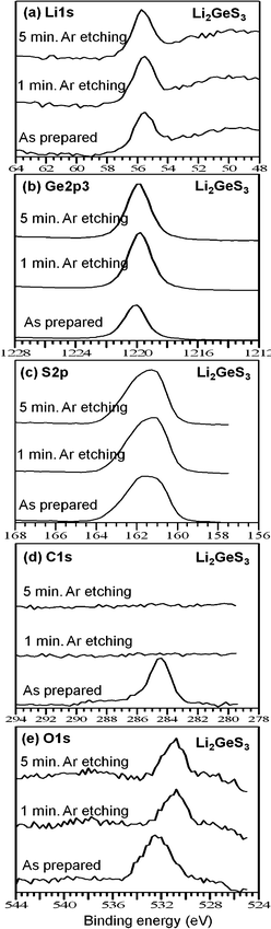 | ||
| Fig. 4 XPS spectra of the Li2GeS3 thin films in Ar atmosphere without Ar etching and with Ar etching for 1 min and 5 min. | ||
The intensity of the C1s XPS spectra decreased to zero after Ar etching and this suggests that the thin films were contaminated by C only in the top 1 nm of the surface. The spectral intensity of the O element decreased after Ar etching treatment as well as and its binding energy shifted to lower values. This suggests that the Ar etching treatment destroys the surface oxygen bonding structure and removed O from the thin film. The XPS spectra of the Li4GeS4 and Li6GeS5 thin films, as-prepared, and with Ar etching for 1 and 5 min show very similar patterns to those of the Li2GeS3 spectra. The two XPS spectra of the as-prepared and with Ar etching of the Li4GeS4 and Li6GeS5 thin films are available in the ESI.† From these spectra, as mentioned above, the thin films were contaminated by C only in the top 1 nm of the surface and were contaminated by O with much lower amounts in the interior of the films. In order to correct the peak positions of the XPS spectra, the C1s peak (284.5 eV) was used for the raw materials before Ar etching. However, after Ar etching was performed, the C1s peak disappeared. For the correction of the peak position after Ar etching, the peaks were shifted by the same amount as used before Ar etching. The different samples were installed together on one sample holder and the XPS spectra were collected before and after Ar etching using the exact same conditions. Thus, it can be anticipated that peak position correction after Ar etching using same amount as shifted for the before Ar etching are reasonable.
In order to determine the fractions of NBS and BS in the thin films, the deconvoluted S2p core peaks for the Li2GeS3, Li4GeS4, and Li6GeS5 as-prepared thin films (without Ar etching treatment) are shown in Fig. 5. While the XPS spectra of the Li, Ge, and S species are unchanged in binding energy with and without Ar etching, Ar etching could reform the chemistry of the Ar sputtered surface. For this reason, it is believed that a better representation of the bonding chemistries, the chemical speciation, of these thin films are therefore found in the as-prepared surfaces of the thin films. For example, Foix et al. reported the fractions of NBS and BS in lithium thio-germanate and thio-arsenate bulk glasses and to do so they broke the glasses in the glove box and they characterized the newly exposed broken surface of the glasses without Ar etching.24–25 In addition, Atashbar et al. reported the XPS deconvoluted data of TiO2 thin films without Ar etching.28
 | ||
| Fig. 5 Deconvoluted S2p core peaks of the Li2GeS3, Li4GeS4 and Li6GeS5 thin films grown in Ar atmosphere. | ||
These approaches suggest that although accurate compositional data could be obtained from the Ar etched surface, a better approach is to use the XPS deconvoluted structural analysis obtained from the as-prepared surface without Ar etching. The fractions of the NBS and BS in the thin films were calculated from Fig. 5 and are shown in Table 5. In Fig. 5 as described above, the Li2GeS3 thin film shows two doublets. The doublet on the low energy side (lower binding energy) is attributed to the NBS and the other doublet on the high energy side (higher binding energy) is associated to BS. The ratios of the NBS and BS in the Li2GeS3 thin film are 64.4% NBS and 35.6% BS, respectively. Although the ratios are not exactly the same as the expected values, 67% NBS and 33% BS, the differences between those of the Li2GeS3 thin film and expected values are within the error range of ±3%. In addition, the ratios of the NBS and BS in the Li2GeS3 target and thin film are very close. This suggests that the target compositions and thin film compositions are quite consistent. While the deconvoluted S2p core spectra of the Li2GeS3 thin film show two doublets, the deconvoluted S2p core spectra of the Li4GeS4 and Li6GeS5 thin films show only one doublet. As described above, the Li4GeS4 and Li6GeS5 targets also show only one doublet from the NBS. In agreement with these Li4GeS4 and Li6GeS5 targets, the two thin films show only one doublet arising from only NBS structures. Recently, a few XPS studies of Ge–S thin films have been reported in the literature but the analyzes were very brief.29–30 However, in this study, the compositions and chemical shifts of the Li–Ge–S thin films have been thoroughly investigated.29–30
In order to compare the binding energies and chemical shifts of these films, the deconvoluted S2p core peaks for GeS2, Li2S, and three thin films without Ar etching are shown in Fig. 6. The spectrum for GeS2 shows a higher binding energy than those of Li2S and the thin films because the GeS2 is assigned to the BS as described above. As the Li2S content increases, the binding energy of the thin films shifts to lower values than that of GeS2. While the binding energies of the thin films are similar to one another, with the S peak for Li2GeS3 being broader than that for Li4GeS4 and Li6GeS5 due to the presence of both BS and NBS, the binding energies of the thin films slightly shifted to lower values. As expected, the binding energy of the Li2S shows the lowest binding energy of the materials studied here.
 | ||
| Fig. 6 Deconvoluted S2p core peaks of the Li2S, GeS2, Li2GeS3, Li4GeS4 and Li6GeS5 thin films. | ||
Experimental
GeS2 starting material preparation
Glassy GeS2 was prepared by reacting stoichiometric amounts of germanium metal powder (Alfa, 99.999%) and sulfur (Alfa, 99.999%) in an evacuated silica tube at 900 °C. First, a bare silica tube was cleaned with a 2% aqueous ammonium bifluoride, NH4HF2, solution. Surface moisture on the inside of the tube was then removed by passing the tube over a natural gas/oxygen flame. Once this moisture was removed, the valve was closed and the tube was transferred to the glovebox where a previously weighed mixture of appropriate amounts of Ge and S were placed into the tube. The sealed tube was removed from the glove box and the sealed with a gas/oxygen torch under vacuum of ∼4 Pa and a liquid nitrogen trap. The sealed tube was then placed into a furnace held at an angle of ∼5° where it was heated at a rate of 1 °C min−1. from room temperature to 900 °C. The tube was rotated at ∼7 rpm to promote mixing and reaction of the components. After the tube was held at 900 °C for 16 h, it was air quenched to room temperature. The air quenched GeS2 material inside the silica tube was put into the glovebox and silica tube was broken to remove the GeS2 glassy product. The final product from this process was a homogeneous, transparent yellow colored glass.Preparation of the target materials
To prepare the Li2GeS3, Li4GeS4, and Li6GeS5 target materials, stoichiometric amounts of Li2S (Alfa, 99.9%) and GeS2 were used. These powders were vibratory Spex milled for ∼15 min inside a steel container with one steel grinding ball inside the glovebox to ensure good mixing and to start the reaction process. Batches of 3 to 4 grams were melted in a covered vitreous carbon crucible at 950 °C for ∼15 min inside a mullite tube lined muffle furnace attached hermetically to the side of the glovebox. The melted charge was poured out of the crucible onto a brass plate and allowed to cool to room temperature. Once enough material, ∼15 g, was prepared, the material was vibratory Spex milled again for 15 min to make fine powder. Fifteen grams of the powder was weighed out and transferred into a hardened steel 2′′ diameter die set. The top press was placed into the die set and allowed to settle on top of the powder. The die set assembly was placed on a sheet of 1/4′′ rubber between the press and the die set and loaded and held at ∼60 MPa overnight. The target was attached to a 2′′ diameter and 0.125′′ thick copper backing plate using silver paste so that it could be water cooled during the RF deposition process to prevent overheating.Substrate preparation
Single crystal silicon substrates, 1 cm × 1 cm × 360 μm, cut and polished along the [111] plane were put into a “piranha” solution (H2SO4:H2O2 = 3:1) for 1 h, ultrasonically cleaned with acetone for 20 min, and then rinsed with deionized water for 20 min. The samples were dried with high purity N2 gas. The samples were put in a drying oven at 120 °C overnight to dry. The cleaned silicon substrates were loaded into a d.c. sputtering chamber in the glovebox and a Ni adhesion layer of ∼120 nm thickness was grown over ∼40 min at ∼3 nm min−1 on the surface of the silicon substrates. The Ni/Si substrates were then loaded into the RF magnetron sputtering chamber on which the thin films were grown.
Thin-film depositions
In order to produce the desired thin films, the target assembly was attached to the sputtering gun inside a high quality (<5 ppm O2 and H2O) glovebox and the sputtering gun assembly was then attached to the sputtering system by removing it from the glovebox and quickly attaching it to the deposition chamber to minimize oxidation of the target. The deposition chamber was then evacuated to ∼9 × 10⁻⁵ Pa during which the deposition chamber was heated for two days using tape heaters to drive off any remaining surface physisorbed water in the system. Substrates were then introduced into the deposition chamber through the glovebox via a sliding track load-lock system. A “sputtering up” configuration was used where the target and sputtering gun were placed below the substrate. In this way, if particles fractured off the target during sputtering they would remain on the target and not contaminate the substrate. In this configuration, it was found that these ceramics targets would crack during extended sputtering, but they could continue to be used for sputtering.Fig. 7 shows a schematic side view diagram of the sputtering system which is connected to the N2 filled glovebox. After pump down and bake out, the sputtering chamber was filled with high purity Ar gas (99.9999%) to ∼13 Pa and the plasma was lit by turning on the RF power to the target. Pre-sputtering was performed for ∼30 min on the target with the substrate shielded in order to clean the surface of the target of any impurities from the brief exposure to air during assembly. After pre-sputtering, all films were produced with a power level of 50 W and a ∼3.3 Pa dynamic pressure of the Argon sputtering gas. Lower pressures and lower powers were found to produce Li deficient films, whereas higher powers were found to quickly and severely degrade the sputtering target.
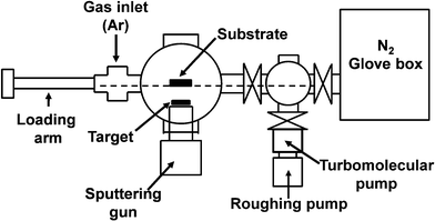 | ||
| Fig. 7 A schematic side view diagram of the sputtering system which is connected to the N2 filled glovebox. | ||
XPS analysis
X-ray photoelectron core level spectra were obtained using a Scienta ESCA-300 spectrometer with monochromatic Al-Kα (1486.6 eV) radiation. Photoelectron spectra were determined at a take-off angle of 45°. The pressure inside the chamber was ∼6.7 × 10⁻¹⁰ Pa at room temperature. The binding energy scale was calibrated by the C1s peak position (284.5 eV). However, after Ar etching treatment was performed, the C1s peak disappeared. Therefore, corrected peaks after Ar etching were obtained by shifting the energies by the same amount as before Ar etching. The XPS intensity scale and sensitivity factors were calibrated by using standard materials. For the sensitivity factors of the Li, Ge, O and S, Li2O, LiF, Li2SO4, GeO2, and GeS2 were used. The starting materials, glassy GeS2 and crystalline Li2S powder, were characterized by XPS to calibrate Li, Ge, and S and to determine the chemical shift limits for the bridging (purely covalent sulfur),Ge–S–Ge, and the purely ionic sulfur, Li+S2−Li+. In addition, XPS was performed on the bulk pressed Li2GeS3, Li4GeS4, and Li6GeS5 target materials, and thin films Ar sputtered from these target materials in order to determine the composition as well as the nature of the chemical bonding (chemical speciation) for each element. The target material, in a compacted powder pellet, was fractured and scraped in the glovebox before loading it into the XPS chamber so as to provide a fresh, nearly uncontaminated surface. After being sputtered, the thin films on Ni/Si substrates were moved directly into the XPS chamber in tightly closed XPS sample containers. In order to get more accurate compositional data, Ar etching for 1 min and 5 min at ∼1 nm min−1etching rate were performed to remove unavoidable residual contaminants on the surface.
Conclusions
The purpose of this work was to provide information on the compositional data and the structures of lithium thio-germanate thin films by means of XPS studies. High purity starting materials were used and targets were produced under well calibrated and optimized conditions. For the first time, highly reproducible compositions and chemical shifts of the starting materials, targets, and thin films of nLi2S + GeS2 materials were determined by XPS. The experiments were done with care to prevent contamination and the RF sputtering conditions were optimized to produce thin films whose compositions agreed quite well with those of the targets. Although the as-prepared thin films contained C and O on the surface, the thin films after Ar etching for 1 min showed that the C was completely removed and O content decreased significantly. This suggests that the thin films were contaminated by C only at the top 1 nm of the surface and the thin films contained low oxygen contents in the interior of the film. After Ar etching, the compositions of the thin films were very close to those expected. Therefore, the thin films produced by sputtering are very close to their corresponding target materials. Thio-germanate thin film materials have not been as widely studied as their oxide materials because of the difficulties in preparation. However, in this study, the lithium thio-germanate thin films were successfully prepared and the compositional data and the chemical shifts were carefully characterized by XPS.Acknowledgements
This research was supported by NSF under grant number DMR-0312081 and this research support is gratefully acknowledged. The authors thank Mr. James Anderegg who helped collect all of the XPS spectra and assisted with the experimental details to load and examine the samples without contamination.References
- C. K. Dyer, J. Power Sources, 2002, 106, 31 CrossRef CAS
.
- S. Prakash, W. E. Mustain and P. A. Kohl, J. Power Sources, 2009, 189, 1184 CrossRef CAS
- N. J. Dudney, Mater. Sci. Eng., B, 2005, 116, 245 CrossRef
- J. M. Tarascon and M. Armand, Nature, 2001, 414, 359 CrossRef CAS
- J. L. Souquet and M. Duclot, Solid State Ionics, 2002, 148, 375 CrossRef CAS
- J. N. Harb, R. M. LaFollette, R. H. Selfridge and L. L. Howell, J. Power Sources, 2002, 104, 46 CrossRef CAS
- M. Dolle, L. Sannier, B. Beaudoin, M. Trentin and J. M. Tarascon, Electrochem. Solid-State Lett., 2002, 5, A286 CrossRef CAS
- X. Yu, J. B. Bates, J. G. E. Jellison and F. X. Hart, J. Electrochem. Soc., 1997, 144, 524 CrossRef CAS
- J. B. Bates, N. J. Dudney, B. J. Neudecker, F. X. Hart, H. P. Jun and S. A. Hackney, J. Electrochem. Soc., 2000, 147, 59 CrossRef CAS
- S. Kondo, K. Takada and Y. Yamamura, Solid State Ionics, 1992, 53–56, 1183 CrossRef CAS
- F. Mizuno, A. Hayashi, K. Tadanaga and M. Tatsumisago, Adv. Mater., 2005, 17, 918 CrossRef CAS
- H. Morimoto, H. Yamashita, M. Tatsumisago and T. Minami, J. Am. Ceram. Soc., 1999, 82, 1352 CrossRef CAS
- E. Robinel, B. Carette and M. Ribes, J. Non-Cryst. Solids, 1983, 57, 49 CrossRef CAS
- Y. Kim, J. Saienga and S. W. Martin, J. Phys. Chem. B, 2006, 110, 16318 CrossRef CAS
- J. Saienga and S. W. Martin, J. Non-Cryst. Solids, 2008, 354, 1475 CrossRef CAS
- W. L. Yao and S. W. Martin, Solid State Ionics, 2008, 178, 1777 CrossRef CAS
- N. Aotani, K. Iwamoto, K. Takada and S. Kondo, Solid State Ionics, 1994, 68, 35 CrossRef CAS
- J. H. Kennedy and Y. Yang, J. Solid State Chem., 1987, 69, 252 CrossRef CAS
- R. Mercier, J.-P. Malugani, B. Fahys and G. Robert, Solid State Ionics, 1981, 5, 663 CrossRef CAS
- A. Pradel, T. Pagnier and M. Ribes, Solid State Ionics, 1985, 17, 147 CrossRef CAS
- J. L. Souquet, E. Robinel, B. Barrau and M. Ribes, Solid State Ionics, 1981, 3–4, 317 CrossRef CAS
- R. Creus, J. Sarradin, R. Astier, A. Pradel and M. Ribes, Mater. Sci. Eng., B, 1989, 3, 109 CrossRef
- M. Yamashita, H. Yamanaka and H. Wakabayashi, Solid State Ionics, 1996, 89, 299 CrossRef CAS
- D. Foix, D. Gonbeau, G. Taillades, A. Pradel and M. Ribes, Solid State Sci., 2001, 3, 235 CrossRef CAS
- A. B. Volynsky, A. Y. Stakheev, N. S. Telegina, V. G. Senin, L. M. Kustov and R. Wennrich, Spectrochim. Acta, Part B, 2001, 56, 1387 CrossRef
- D. Foix, D. Gonbeau, D. Granier, A. Pradel and M. Ribes, Solid State Ionics, 2002, 154, 1613 CrossRef
- V. Yufit, M. Nathan, D. Golodnitsky and E. Peled, J. Power Sources, 2003, 122, 169 CrossRef CAS
- M. Z. Atashbar, H. T. Sun, B. Gong, W. Wlodarski and R. Lamb, Thin Solid Films, 1998, 326, 238 CrossRef CAS
- D. Gonbeau, V. Pamukchieva, R. Dedryvere, E. Skordeva and D. Arsova, J. Optoelectron. Adv. Mater., 2005, 7, 341 CAS
- M. Mitkova, M. N. Kozicki, H. C. Kim and T. L. Alford, Thin Solid Films, 2004, 449, 248 CrossRef CAS
Footnote |
| † Electronic supplementary information (ESI) available. See DOI: 10.1039/c1ra00165e |
| This journal is © The Royal Society of Chemistry 2011 |