Synthesis of tin nanodendrites via galvanic replacement reaction and their thermal conversion to nanodendritic tin oxide for ultrasensitive electrochemical sensing†
Wenzhao
Jia
a,
Liang
Su
a,
Xiaopeng
Li
b,
Lichun
Zhang
c,
Zhiyong
Gu
b,
Pu-Xian
Gao
c and
Yu
Lei
*a
aDepartment of Chemical, Materials and Biomolecular Engineering, University of Connecticut, 191 Auditorium Road, Unit 3222, Storrs, CT 06269, USA. E-mail: ylei@engru.uconn.edu; Fax: +1(860)486 2959; Tel: +1(860)486 4554
bDepartment of Chemical Engineering and Nanomanufacturing Center, University of Massachusetts–Lowell, One University Avenue, Lowell, MA 01854, USA
cInstitute of Material Sciences, University of Connecticut, 97 North Eagleville Road, Unit 3136, Storrs, CT 06269, USA
First published on 6th October 2011
Abstract
Tin nanodendrites have been fabricated using galvanic replacement reaction between stannous chloride (SnCl2) and thermal evaporated zinc film composed of Zn nanodiscs. The replacement reaction is completed in a few seconds, and the produced Sn nanodendrites possess a single crystalline structure. The growth process of Sn nanodendrites is studied by changing the concentration of SnCl2 in the replacement reaction, and the growth direction is identified by electron diffraction analysis. The as-prepared Sn nanodendrites are further oxidized by rheotaxial growth and thermal oxidation (RGTO) process to generate tin oxide nanodendrites. The electrochemical properties of SnO2 nanodendrites are demonstrated in the electrocatalytic reaction of hydrogen peroxide (H2O2), and the reduction of H2O2 is tremendously enhanced in terms of the onset potential and the magnitude of reduction current. The amperometric H2O2 sensor, using the as-prepared SnO2 nanodendrites as the electrochemical catalyst, shows a wide linear range, a good limit of detection, a high sensitivity, and good reproducibility. This study provides a promising route to the facile synthesis of functional metals/metal oxides with unusual nanostructures, which have great potential in sensing applications.
1. Introduction
The synthesis of nanostructured metals and metal oxides has been receiving intense interest because of their unique and/or superior catalytic, electronic, photonic, and magnetic properties.1,2 In the past decade, nanomaterials with various shapes (e.g.nanowires, nanotubes, nanodiscs, etc.) have been successfully synthesized, and their chemical and physical properties are found to be strongly dependent on the size and shape of nanomaterials. Additionally, nanomaterials with several new geometric configurations have also been reported, such as nanohelixes,3 zigzag nanobelts,4 and more complicated 3D structures. Up to date, a number of techniques have been developed for preparing nanostructured metals/metal oxides with controllable size and shape. For instance, the chemical reduction of a metal precursor by a reducing agent in the solution phase, with or without the aid of a surfactant and/or a stabilizer, is extensively applied to control the morphology of the nanostructured metals;5,6 electrochemical reduction of metal precursors is another widely used method in this regard. The synthesis of metal oxide nanostructures can be obtained through the thermal evaporation of corresponding metal sources with an oxygen supply.7Recently, a facile method, galvanic replacement, has been used as an amazingly simple and effective alternative to prepare noble metal or metal alloy nanostructures based on the electrical potential difference between two metals.8 Generally, metal nanostructures with higher reactivity are synthesized first, and serve as sacrificial templates. Metals with lower reactivity are then replaced from their salt precursors by the active metal templates. The degree of the replacement reaction depends on the size of metal templates, the amount of metal salts, and reaction time.9,10 For instance, silver (Ag) nanoparticles with a 13 nm diameter can be completely transformed into gold or palladium if the precursors of gold (Au) or palladium (Pd) are sufficient, otherwise alloys are formed.11,12Ag nanowires were used to displace Pt or PtPd to form the corresponding nanotubes, which demonstrated good catalytic activity towards oxygen reduction reactions.13Pb nanowires were obtained by the replacement reaction of Pb ions on zinc foils.14 Furthermore, it has been found that thiourea can decrease the standard potentials of metals, which has made the replacement process of copper by tin possible.15 However, it is unclear whether the replacement reaction with the involvement of highly active metals could form novel nanostructures.
In this paper, we address these queries and report on the synthesis of Sn nanodendrites by employing zinc nanodiscs for the replacement reaction. Zn can be spontaneously replaced by Sn in a normal aqueous solution according to their standard potentials:
| Sn2+ + 2 e− = Sn E0 = −0.140 V | (1) |
| Zn2+ + 2 e− = Zn E0 = −0.7618 V | (2) |
2. Experimental
Synthesis of Zn films and Sn nanodendrites: A thin layer of zinc was coated onto a glass substrate using a thermal evaporator (NTE-3000) of zinc (99.993%, Alfa Aesar) at the vacuum level of 10−6 torr. The deposition rate was controlled at 1 Å per second and the final thickness of the zinc layer was 65 nm. The as-prepared metallic films were directly used for the replacement reaction. Stannous chloride (SnCl2, Fisher) was dissolved in water to prepare aqueous solution right before use. Glass substrate with Zn film was immersed into the SnCl2 solution for several seconds to complete the replacement reaction. The substrates were then carefully rinsed with DI water.Thermal conversion of Sn nanodentrites to tin oxide nanodendrites: To oxidize metallic films, the substrates were heated in a muffle furnace, or a tube furnace with an oxygen supply. The heating process follows a two-step procedure: 2 h at 200 °C and then 4 h at 700 °C.
Material characterization: A JEOL 6335F field emission scanning electron microscope (FESEM) was employed to examine the morphology of the as-prepared samples. The crystal structures of the samples were characterized by Oxford diffraction XcaliburTM PX Ultra with ONYX detector. A Tecnai T12 TEM was used for morphological imaging. HRTEM, selected-area electron diffraction (SAED) and micro-area electron diffraction were carried out with a JEOL 2010 FasTEM.
Detection of hydrogen peroxide by tin oxide nanodendrites: A glassy carbon electrode (GCE, dia. 3 mm) was first polished with alumina slurries (1 μm and 0.05 μm) and then cleaned by sonication in ethanol, acetone, and water successively. The SnO2 nanodendrites were carefully scratched off from substrate and suspended in ethanol. The concentration of SnO2 nanodendrites was determined using quartz crystal microbalance. 5 μL of SnO2 nanodentrite suspension was then dropped onto GCE. After ethanol was completely evaporated, 5 μL of 0.5 wt% Nafion was used to entrap the nanodendrites. The electrodes are denoted as SnO2/Nafion/GCE. The Nafion coated GCE (Nafion/GCE) was also prepared as a control electrode. All electrochemical experiments were performed using a standard three-electrode configuration consisting of a working electrode, an Ag/AgCl reference electrode, and a platinum disc counter electrode. The cyclic voltammetry (CV) was performed in a 0.1 M phosphate buffer (pH 7.4) in the absence and presence of 2 mM H2O2 utilizing an electrochemical workstation (CHI-601) at a scan rate of 50 mV/s. For amperometric detection, all measurements were performed by applying an appropriate potential (vs.Ag/AgCl reference) to the working electrode and allowing the transient background current to decay to a steady-state value, prior to the addition of H2O2. The current response resulting from the addition of H2O2 was recorded. A stirred solution was employed to provide convective transport.
3. Results and discussion
3.1. Tin nanodendrites
Due to its low standard potential, Zn was chosen as the more active metal in the replacement reaction. Zn film was prepared by vacuum thermal evaporation due to its low melting point. A typical SEM image of Zn film is shown in Fig. 1A. It can be seen that the zinc film is composed of well-faceted hexagonal Zn nanodiscs with a diameter of 650 nm. A higher magnification SEM image of a twinned Zn nanodisc is shown in Fig. 1B. It can be found that the Zn nanodisc has a smooth surface, and is packed with several layers of Zn platelets with a typical thickness around tens of nanometres. This result is consistent with the observation from Guo, et al.20Fig. 1C shows a typical TEM image of two overlaid Zn nanodiscs, which clearly shows the layered structure of Zn nanodiscs from the edge contrast. The SAED pattern (Fig. 1D) indicates that the Zn nanodisc is single-crystalline dominated by (0001) crystal facets, which is the most stable facet intrinsically.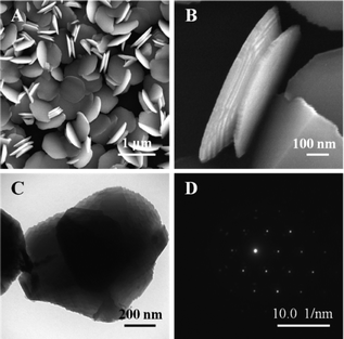 | ||
| Fig. 1 A typical FESEM image of Zn nanodiscs; B. A high magnification side-view of a twinned Zn nanodisc; C. A TEM image of Zn nanodiscs; D. The SAED pattern of Zn nanodiscs. | ||
Zn is an active material in the activity series of metals, therefore it can displace many metals which are lower in the series. For example, tin, which is slightly less active than Zn, can be replaced by Zn. In this study, stannous chloride (SnCl2) is used as the source of tin ions. When the replacement reaction occurred, the color of the Zn film immediately changed from silvery gray to a darker grey in a few seconds, indicating the formation of Sn. XRD was carried out to reveal the crystal structure of the replacement product. Comparing XRD pattern a with b in Fig. 2, it was found that all the peaks after the replacement reaction can be assigned to tetragonal Sn (JCPDS 4-673), while no peak correlated with Zn (JCPDS 4-831) was observed, indicating that this displacement process was completed within several seconds.
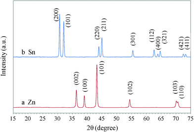 | ||
| Fig. 2 XRD patterns of Zn nanodiscs (a) and Sn nanodendrites (b). | ||
The SEM image in Fig. 3A shows the typical morphology of the as-synthesized Sn. Interestingly, the products display a dendrite-like structure. The main stem of the dendrite is typically 350–450 nm in diameter, and the branches are about 150–250 nm, which grow almost perpendicular to the main stem. The Sn rods of both main stem and branches have a faceted and sectional structure (Fig. 3A inset). Fig. 3B shows a TEM image of a Sn nanodendrite and the corresponding SAED pattern from the edge of a branch, which reveals that the architectures are solid and the dendrite Sn is single-crystalline. Further investigation was performed by micro-area electron diffraction analysis in TEM to find out the growth direction. Analysis was conducted on both sides of branches and the main stem, and the patterns obtained were the same for all the selected regions (Fig. S1), indicating the single crystalline dendrite with growth direction along [220]. By controlling reaction conditions, no tin nanodiscs or nanodiscs with a hollow interior could be formed. One possible reason is that during the replacement reaction, Zn is replaced by Sn and Sn grows along its own preferential direction.
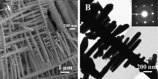 | ||
| Fig. 3 A. FESEM image of Sn nanodentrites. The inset is a high magnification SEM image of the branches; B. TEM image of Sn nanodentrite. The inset is the SAED pattern. | ||
A dendritic structure has been reported previously from the replacement reaction between Ag+ and Zn plates.21 Basically, the formation of dendrites is usually a diffusion control process, in which the particles are more easily captured by the tip parts. In our case, since the Zn nanodiscs are very thin, the longitudinal diffusion (perpendicular to the film surface) is negligible, while transverse walking (parallel to the surface) of Sn2+ should be dominant. In order to have a clearer view of the growth process, diluted SnCl2 solutions were used to react with the Zn film, given that this replacement reaction is too fast (less than several seconds) to study the evolution of Sn nanodendrites. A series of SnCl2 concentrations ranging from 0.01 M to 1 M were examined. When the concentration of Sn precursor was 0.01 M, no obvious geometry could be observed, and only nanoparticles with irregular morphology were generated (Fig. 4A). When the concentration of SnCl2 increased to 0.1 M, the majority of the products had a faceted structure, while only few of them showed shorter dendritic structure (Fig. 4B and inset). With a further increase of SnCl2 concentration to 0.5 M, dendritic Sn formed (Fig. 4C), but the amount was lower than those observed with 1 M SnCl2 (Fig. 3A). In addition, it is clearly observed from Fig. 4C that some sub-branches also grew from the branches to form a more complicated structure. Theoretically, material growth has large consequences in regards to its own properties with a minimal surface energy or lower energy barrier, and the shape produced by faster growth along energetically favorable crystallographic directions.22 For this reaction, (220) type low-index surfaces of Sn are likely to have the lowest energy, and the high concentration of Sn2+ would possibly induce the anisotropic growth along [220] to form dendrites. Additionally, single-crystalline Zn may also direct the formation and growth of Sn dendrites.23 As growth proceeds, branches are initiated with sufficient amount of Sn source from the stem to form a dendrite structure. Compared with other replacement reactions, the fast reaction rate is probably due to the reasons that both Sn and Zn are active metals and possess quite different standard potentials (driving force).13
 | ||
| Fig. 4 FESEM images of Sn nanostructures prepared through replacement reaction between Zn nanodiscs and SnCl2 with different concentration: A. 10 mM SnCl2. B. 100 mM SnCl2. C. 500 mM SnCl2; all scale bars are 1 μm. | ||
3.2. Tin oxide nanodendrites
Thermal oxidation is one of the most commonly employed approaches to synthesize novel nanostructured metal oxides from metals.24 Since tin dioxide is an important semiconductor with unique optical and electrical properties, there are a number of reports regarding the thermal oxidation of Sn to SnO2. As Sn has a low melting temperature, the rheotaxial growth and thermal oxidation (RGTO) process was developed with the aim of retaining the morphology of the original Sn after its conversion, which has been widely used to prepare SnO2 nanowire, nanodiscs or films.25 In this study, the as-prepared nanodendritic Sn was first heated to 200 °C (lower than 232 °C, the melting temperature of bulk tin), and maintained at this temperature for 2 h to oxidize the surface layers as a supporting sheath to retain the structures, followed by heating up to 700 °C to completely oxidize the samples. XRD analysis was conducted to examine the oxidation process. As shown in Fig. 5, different phases of tin oxides are observed at different temperatures. With the increase of temperature, it was found that the film of Sn changed to brownish, and from XRD data, the extra peaks mainly from tetragonal SnO (JCPDS 06-0395, a = b = 0.3802 nm, c = 0.4836 nm) first appeared along those from Sn. With further increase of temperature, the reflections associated with SnO increased in intensity, while Sn diffraction peaks disappeared and a complete transformation of Sn to SnO was observed when maintaining the temperature at 350 °C (Fig. 5b). When the temperature went up to 500 °C, the sample became white color, demonstrating that another phase of oxides was formed, and SnO2 was observed and coexisted with SnO in the XRD pattern. When the temperature reached 700 °C, the XRD study shows that the sample was completely oxidized to form SnO2. However, surprisingly, two forms of SnO2, tetragonal (JCPDS 29-1484) and orthorhombic (JCPDS 41-1445), were observed in the final products (Fig. 5c). To rule out the oxygen effect, thermal treatments were also conducted with either air or just pure O2 flow throughout the whole oxidation process (Fig. 5d). Same patterns of the product were found, so that the difference of oxygen concentration and oxidation time may not be the crucial factors leading to the formation of two crystalline structures of SnO2. The reasons are still unclear, but similar phenomena has been observed by other groups.26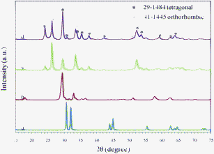 | ||
| Fig. 5 XRD patterns for the oxidized products obtained at different temperature: Sn nanodendrites (a) were heated to 350 °C in air (b), 700 °C in air (c), and 700 °C in O2 (d). | ||
As shown in Fig. 6A, the products obtained after thermal treatment at 700 °C maintain the dendritic structures of Sn, but the surface became granular. The branches slightly deform probably due to the molten low-melting-point of Sn when the temperature is higher than 232 °C. TEM was further employed to study the oxidized samples. Since the dendrites adhered strongly to the substrate after thermal treatment, the samples were carefully scratched off from substrate to prepare the TEM samples, so that the structures may be destroyed to some extent (Fig. 6B). Moreover, granular structures were clearly observed on the surface of the SnO2 nanodendrites. The thermal oxidation process may be described as follows: in an oxygen environment and at an elevated temperature lower than the melting temperature of Sn, the oxidation starts at the surface of the Sn particles, and SnO phases are nucleated and formed as dispersed clusters on the surface of Sn. SnO would decomposed into Sn3O4 and Sn during heating treatment when oxygen is controlled by diffusion control.27 With further increase of temperature, the Sn3O4 decomposes into SnO2 and Sn. The SnO2 keeps on growing from the surface to the core while the Sn is continuously oxidized when oxygen is diffused into the inside of dendrites.28 Finally, SnO2 nanodentrites were formed with the same morphology of the Sn precursor.
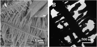 | ||
| Fig. 6 A typical SEM image (A) and a typical TEM image (B) of tin oxide nanodendrites; inset of Figure A is a high magnification SEM image of branches with a scale bar of 200 nm. | ||
3.3. Tin oxide nanodendrites for electrochemical sensors
Tin and tin oxide are important materials with promising applications in many fields.29,30 The nanodendrites generated by this method have highly branched structures and high surface area, which are suitable for catalysis. The electrocatalytic activity of the as-prepared SnO2 architectures was thus evaluated by cyclic voltammogram (CV). H2O2 was selected as a model compound because it is a product of enzymatic reactions catalyzed by a large number of oxidases, and is practically important in the field of biosensor development. Fig. 7 displays the CVs in the absence and presence of 2 mM H2O2 as recorded with SnO2/Nafion/GCE and a Nafion/GCE, respectively. The CV of the Nafion/GCE only shows a very small background current in buffer, while a dramatic increase of current signal towards the negative ends of the potential range was observed when the SnO2/Nafion/GCE was used in buffer, which may be attributed to the large surface area and enhanced electron transfer of the as-synthesized SnO2 nanodendrites. Upon the addition of 2 mM H2O2, one can see that no obvious redox response to H2O2 is observed over most of the potential range for Nafion/GCE. However, the reduction currents were greatly enhanced due to the strong electrocatalytic reaction of H2O2 for SnO2/Nafion/GCE, whereas there is no significant enhancement towards the oxidation of H2O2 in the examined region. The reduction process starts at ca. 0 V (vs.Ag/AgCl). Compared to Nafion/GCE, SnO2 nanodendrite-modified electrode offers a positive shift in the cathodic overpotential for H2O2 reduction, which may be owing to a substantial increase in the electron transfer rate for the reduction of H2O2 probably resulting from the enhanced kinetic and transport effect of H2O2 at the SnO2/Nafion/GCE interface. In addition, tin oxide has been well studied for its surface oxygen depletion property.31 At a negative potential, the tin oxide nanodendrites tend to be in a more reduced state, which may facilitate the absorption of oxygen atoms in H2O2, and thus enhance the electron transfer to reduce H2O2.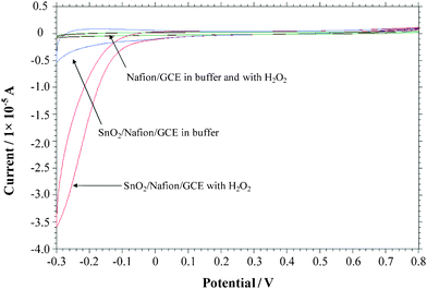 | ||
| Fig. 7 Cyclic voltammograms of the Nafion/GCE and the SnO2/Nafion/GCE electrode in 0.1 M pH 7.4 phosphate buffer in the absence and presence of 2 mM H2O2, respectively. Scan rate = 50 mV s−1. | ||
In order to study the effect of applied potentials on electrocatalytic reduction of H2O2 at the SnO2 nanodendrites-modified electrode, the amperometric responses to successive additions of H2O2 were recorded with respect to different applied potentials (Fig. 8). As the reduction of H2O2 for SnO2/Nafion/GCE starts at 0 V and increases significantly towards the negative ends, stepwise current responses to H2O2 at −0.1V were observed as expected (Fig. 8A). In addition, the reduction currents increase sharply with further decrease of applied potentials (Fig. 8B and C). For all the applied potentials, the SnO2/Nafion/GCE responds rapidly to the changes in H2O2 concentration, producing steady-state signals within 10 s. The amperometric results match the CVs results well. The corresponding calibration curves are presented in Fig. 8D and the analytical characteristics such as the linear range, sensitivity and the limit of detection (LOD) were summarized in Table 1. One can see that the highest sensitivity (265.6 μA mM−1 cm−2) and the widest linear range (up to 2.7 mM) were obtained at an applied potential of −0.3 V. However, the best limit of detection (59 nM) at a signal-to-noise of 3 was achieved at an applied potential of −0.1 V because of the lowest noise level at −0.1 V. This LOD is very impressive and significantly better than recently reported H2O2 sensors.32–36 For a higher concentration of H2O2, the plot deviates from linearity, which may be attributed to the saturation of the electrocatalytic activity of SnO2 nanodendrites (Fig. 8D). The repeatability was examined by recording the responses from 30 μM of H2O2 injection. The standard deviations were 6.37%, 8.79%, and 9.59% at the applied potential of −0.1, −0.2, and −0.3 V, respectively, indicating the good repeatability of the H2O2 detection. It can be seen that the performance of the developed sensor is superior compared with most of H2O2 sensors in literature. Specifically, the sensitive detection of H2O2 at a negative applied potential can greatly minimize the intervention from interferences such as acetaminophen, uric acid and ascorbic acid, which are not electroactive at such low applied potential, and thus has the potential to enhance the selectivity in the (bio)sensor development.
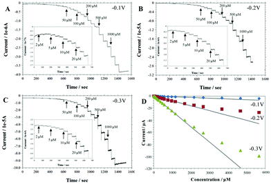 | ||
| Fig. 8 Amperometric response of the SnO2/Nafion/GCE with successive additions of H2O2 to 0.1 M pH 7.4 phosphate buffer at an applied potential of −0.1 V (A), −0.2 V (B), and −0.3 V (C), respectively; D. The corresponding calibration curves. Insets show the amperometric response in low concentration range. | ||
| Applied potential (V vs.Ag/AgCl) | Linear range up to (mM) | Sensitivity (μA mM−1cm−2) | Detection limit (μM) |
|---|---|---|---|
| −0.1 | 1.2 | 14.44 | 0.059 |
| −0.2 | 1.7 | 90 | 0.36 |
| −0.3 | 2.7 | 265.6 | 0.60 |
Conclusions
In summary, single-crystalline Sn nanodendrites have been synthesized by displacement reaction with thermally evaporated Zn nanodiscs. The Sn nanodendrites grow along [002] directions. Through a RTGO process, the as-prepared Sn nanodendrites are further oxidized to form oxides which retain nanodendritic structures and consist of tetragonal and orthorhombic SnO2. The SnO2 nanodendrites have exhibited enhanced catalytic property toward hydrogen peroxide reduction. Rapid, sensitive and repeatable amperometric detection of H2O2 has been achieved at the SnO2 nanodendrite modified electrode. This study provides a simple way to synthesize unusual nanostructures which have great potential in various applications ranging from catalysts to sensors.References
- J. Y. Liu, T. Luo, T. S. Mouli, F. L. Meng, B. Sun, M. Q. Li and J. H. Liu, Chem. Commun., 2010, 46, 472 RSC.
- W. Z. Jia, L. Su, Y. Ding, A. Schempf, Y. Wang and Y. Lei, J. Phys. Chem. C, 2009, 113, 16402 CAS.
- R. S. Yang, Y. Ding and Z. L. Wang, Nano Lett., 2004, 4, 1309 CrossRef CAS.
- J. H. Duan, S. G. Yang, H. W. Liu, J. F. Gong, H. B. Huang, X. N. Zhao, R. Zhang and Y. W. Du, J. Am. Chem. Soc., 2005, 127, 6180 CrossRef CAS.
- J. Y. Chen, B. J. Wiley and Y. N. Xia, Langmuir, 2007, 23, 4120 CrossRef CAS.
- S. H. Sun, D. Q. Yang, D. Villers, G. X. Zhang, E. Sacher and J. P. Dodelet, Adv. Mater., 2008, 20, 571 CrossRef CAS.
- J. Zhou, Y. Ding, S. Z. Deng, L. Gong, N. S. Xu and Z. L. Wang, Adv. Mater., 2005, 17, 2107 CrossRef CAS.
- X. M. Lu, J. Y. Chen, S. E. Skrabalak and Y. N. Xia, Proc. Inst. Mech. Eng., Part N, 2007, 221, 1 Search PubMed.
- X. W. Teng, Q. Wang, P. Liu, W. Han, A. Frenkel, W. Wen, N. Marinkovic, J. C. Hanson and J. A. Rodriguez, J. Am. Chem. Soc., 2008, 130, 1093 CrossRef CAS.
- Y. G. Sun, B. Wiley, Z. Y. Li and Y. N. Xia, J. Am. Chem. Soc., 2004, 126, 9399 CrossRef CAS.
- Q. B. Zhang, J. P. Xie, J. H. Yang and J. Y. Lee, ACS Nano, 2009, 3, 139 CrossRef CAS.
- Q. B. Zhang, J. P. Xie, J. Liang and J. Y. Lee, Adv. Funct. Mater., 2009, 19, 1387 CrossRef CAS.
- Z. W. Chen, M. Waje, W. Z. Li and Y. S. Yan, Angew. Chem., Int. Ed., 2007, 46, 4060 CrossRef CAS.
- C. Y. Wang, M. Y. Lu, H. C. Chen and L. J. Chen, J. Phys. Chem. C, 2007, 111, 6215 CAS.
- G. F. Cui, X. Ke, H. Liu, J. W. Zhao, S. Q. Song and P. K. Shen, J. Phys. Chem. C, 2008, 112, 13546 CAS.
- N. Q. Jia, Q. Zhou, L. Liu, M. M. Yan and Z. Y. Jiang, J. Electroanal. Chem., 2005, 580, 213 CrossRef CAS.
- E. Topoglidis, Y. Astuti, F. Duriaux, M. Gratzel and J. R. Durrant, Langmuir, 2003, 19, 6894 CrossRef CAS.
- L. Shi, Y. Xu, S. Hark, Y. Liu, S. Wang, L. Peng, K. Wong and Q. Li, Nano Lett., 2007, 7, 3559 CrossRef CAS.
- J. H. He, T. H. Wu, C. L. Hsin, K. M. Li, L. J. Chen, Y. L. Chueh, L. J. Chou and Z. L. Wang, Small, 2006, 2, 116 CrossRef.
- C. F. Guo, Y. S. Wang, P. Jiang, S. H. Cao, J. J. Miao, Z. W. Zhang and Q. Liu, Nanotechnology, 2008, 19, 445710 CrossRef.
- H. J. You, J. X. Fang, F. Chen, M. Shi, X. P. Song and B. J. Ding, J. Phys. Chem. C, 2008, 112, 16301 CAS.
- H. Brune, C. Romainczyk, H. Roder and K. Kern, Nature, 1994, 369, 469 CrossRef CAS.
- Y. Ding, P. X. Gao and Z. L. Wang, J. Am. Chem. Soc., 2004, 126, 2066 CrossRef CAS.
- Z. R. Dai, Z. W. Pan and Z. L. Wang, Adv. Funct. Mater., 2003, 13, 9 CrossRef CAS.
- A. Kolmakov, Y. X. Zhang and M. Moskovits, Nano Lett., 2003, 3, 1125 CrossRef CAS.
- M. O. Orlandi, A. J. Ramirez, E. R. Leite and E. Longo, Cryst. Growth Des., 2008, 8, 1067 Search PubMed.
- K. M. Li, Y. J. Li, M. Y. Lu, C. I. Kuo and L. J. Chen, Adv. Funct. Mater., 2009, 19, 2453 CrossRef CAS.
- N. M. A. Hadia, S. V. Ryabtsev, P. V. Seredin and E. P. Domashevskaya, Phys. B, 2010, 405, 313 CrossRef CAS.
- W. M. Zhang, J. S. Hu, Y. G. Guo, S. F. Zheng, L. S. Zhong, W. G. Song and L. J. Wan, Adv. Mater., 2008, 20, 1160 CrossRef CAS.
- H. T. Chen, S. J. Xiong, X. L. Wu, J. Zhu, J. C. Shen and P. K. Chu, Nano Lett., 2009, 9, 1926 CrossRef CAS.
- M. Batzill, K. Katsiev, J. M. Burst, U. Diebold, A. M. Chaka and B. Delley, Phys. Rev. B, 2005, 72, 165414 CrossRef.
- J. S. Huang, D. W. Wang, H. Q. Hou and T. Y. You, Adv. Funct. Mater., 2008, 18, 441 CrossRef CAS.
- S. J. Guo, S. J. Dong and E. K. Wang, Small, 2009, 5, 1869 CrossRef CAS.
- C.X. Guo, X.T. Zheng, S.R. Ng, Y.C. Lai, Y. Lei and C.M. Li, Chem. Commun., 2011, 47, 2652 RSC.
- J.P. Liu, C.X. Guo, C.M. Li, Y.Y. Li, Q.B. Chi, X.T. Huang, L. Liao and T. Yu, Electrochem. Commun., 2009, 11, 202 CrossRef CAS.
- C.X. Guo, F.P. Hu, C.M. Li and P.K. Shen, Biosens. Bioelectron., 2008, 24, 819 CrossRef CAS.
Footnote |
| † Electronic Supplementary Information (ESI) available: Micro-XRD patterns for the corresponding regions in Sn nanodentrites. See DOI: 10.1039/c1ra00433f/ |
| This journal is © The Royal Society of Chemistry 2011 |
