Water photolysis with a cross-linked titanium dioxide nanowire anode†
Mingzhao
Liu‡
a,
Nathalie
de Leon Snapp‡
a and
Hongkun
Park
*ab
aDepartment of Chemistry and Chemical Biology, Harvard University, 12 Oxford Street, Cambridge, Massachusetts 02138, USA. E-mail: hongkun_park@harvard.edu
bDepartment of Physics, Harvard University, 12 Oxford Street, Cambridge, Massachusetts 02138, USA
First published on 10th September 2010
Abstract
We report efficient water photolysis using a cross-linked TiO2 nanowire anode containing mixed anatase and rutile phases. Under simulated AM 1.5 G illumination, the peak solar energy conversion efficiency is measured to be 1.05%, a new record for TiO2 photoanodes. A photocurrent density as high as 2.6 mA cm−2 is observed when the film thickness is 22 μm. These observations indicate that the high surface area architecture afforded by the cross-linked TiO2 nanowires enables both long optical path lengths and high photon-to-electron conversion efficiency. We also report photocurrent in the visible range due to sub-band gap absorptions, which is enhanced by up to a factor of 10 when the TiO2 nanowires are coated with gold or silver nanoparticles. This enhancement is observed only in thinner (up to 1 μm) TiO2 nanowire films, however, indicating that the effect stems from enhanced light retention by nanoparticle scattering.
Introduction
Efficient artificial photosynthesis, in which energy from sunlight is converted into chemical energy, has been a subject of intense research effort but has remained an elusive goal. Photolysis of water into H2 and O2 is one of the most prominent examples of artificial photosynthesis. It was first achieved by Fujishima and Honda in 1972 using an n-type TiO2 electrode,1 but efforts to develop a more efficient process have generally faltered. Materials whose band gaps are well matched to the solar spectrum are chemically unstable in water and thus unsuitable for photoelectrochemical cells.2,3 TiO2 has a 3 eV band gap and can only absorb ultraviolet light (400 nm or shorter), setting its theoretical maximum energy conversion efficiency at 2.2%.4 Most TiO2-based cells make insufficient use of even the UV spectrum, however, and the peak energy conversion efficiencies reported to date have been 0.6% or less over the whole solar spectrum with incident photon-to-current efficiencies (IPCE) of 10% or less at the band gap.5A primary factor limiting the efficiency of these devices is the mismatch between the optical path length required for light absorption and the charge diffusion lengths. If a photogenerated charge is to participate in a chemical reaction, it must be able to reach the semiconductor/electrolyte interface before it recombines. In an anatase TiO2 film, the film thickness required to absorb 90% of the light above the band gap is on the order of 1 μm,6 but the minority carrier (hole) diffusion length is only around 70 nm.7 Consequently, in a film of sufficient thickness to absorb the majority of incident light, most of the minority carriers recombine before reaching the TiO2/H2O interface.4,8 This consideration highlights the importance of engineering systems with both a high optical density and high surface-to-volume ratio. In this study, we explore two distinct strategies based on cross-linked nanowires to increase the optical density in high surface area structures.
To date, TiO2 anodes composed of nanoparticles and nanowires have been widely explored to improve photolysis efficiency.9–11 These studies have shown that nanostructures provide significantly shorter path lengths for the photogenerated minority carriers to reach the surface, resulting in higher photoconversion efficiencies than bulk or compact thin film devices.9 Unfortunately, the maximum photoconversion efficiency reported in these studies is 0.6% or below because they generally have smaller grain size than compact thin films and thus have low electrical conductivity.12,13 Furthermore, these nanostructures have been predominantly in the anatase phase, which has a larger band gap than rutile (3.2 eV versus 3.0 eV).4 Another strategy that has been explored to improve the photolysis efficiency is to use the plasmon resonance of metallic particles to increase the absorption cross section of a device. Near its surface plasmon resonance, the polarizability of a metallic nanoparticle increases greatly, increasing its absorption and scattering cross sections.14,15 In the near field, the strong electric field enhancement can effectively concentrate light to the surface, leading to a shorter distance for the minority carrier to travel before it reaches the electrolyte interface and less recombination.16,17 In the far field, enhanced scattering of light can lead to longer optical path lengths within the device.18–20
In the present study, we report water photolysis using cross-linked TiO2 nanowire thin films that achieve both long optical path lengths and high incident photon-to-electron conversion efficiencies. Previous work in nanostructured anodes for water photolysis has relied on the synthesis of well-ordered films for electrical continuity to the back contact.9,21 These well-ordered films, however, must be made of thin, highly resistive components in order to maintain high surface area contact with the electrolyte.22 We show that in a film of randomly oriented large diameter nanowires that are chemically cross-linked, we can achieve an optically dense structure that is also highly conductive. The random orientation of the wires also helps to increase the effective optical path length by scattering the light into the plane of the film. Under simulated AM 1.5 G illumination, we find that the peak solar energy conversion efficiency is greater than 1%, and the photocurrent density can be as high as 2.6 mA cm−2. Unlike in compact thin films, the photocurrent density monotonically increases with film thickness up to 22 μm. We have also observed water photolysis with sub-band gap absorption in the visible range, which is enhanced by up to a factor of 10 in TiO2 films up to 1 μm thick by coating them with gold or silver nanoparticles.
Experimental
Preparation of TiO2 nanowires
TiO2 nanowires were synthesized by a method similar to the one reported by Jiang et al.23,24 The titanium precursor solution was prepared by dissolving 0.25 mL titanium butoxide (Ti(O-n-Bu)4) into 5 mL anhydrous ethylene glycol. In a separated flask, 1 g of PVP (polyvinylpyrrolidone, MW ≈ 55,000) was dissolved into 50 mL anhydrous ethylene glycol under dry nitrogen flow. The PVP solution was then heated to 185 °C, at which point the titanium precursor solution was quickly injected. When the mixture was stirred and kept at 175 °C for 3 h, a white precipitate of titanium ethylene glycolate nanowires formed in the solution.23 This precipitate was collected by centrifugation, cleaned by repeatedly washing with water and ethanol, and dried in a 100 °C oven overnight. The dried precipitate was heated to 500 °C in air for 2 h to convert the titanium ethylene glycolate nanowires to TiO2 nanowires. The crystalline nature of these nanowires was confirmed by X-ray diffraction, with a Scintag XDS2000 diffractometer using Cu-Kα radiation (λ = 154.18 pm) at a rate of 0.5° min−1. The morphology of the TiO2 nanowires was characterized using a Zeiss Ultra55/Supra55VP field emission scanning electron microscope.Deposition of TiO2 nanowire thin film
The TiO2 nanowires were dispersed in isopropyl alcohol and drop cast onto a titanium electrode to form a thin film. The thickness was controlled by the number of depositions. The titanium electrode was made by evaporating a layer composed of 10 nm Ti (bottom)/50 nm Pt/120 nm Ti on a clean frosted glass slide. In order to increase the conductivity and mechanical stability of the TiO2 nanowire network, the thin film was cross-linked with 1 atom% of titanium isopropoxide by drop casting the solution. The film was then left in air overnight to allow for hydrolysis of titanium isopropoxide and resultant cross-linking of nanowires. Finally the electrode was annealed at 600 °C in forming gas (95% N2 + 5% H2) for 2 min in order to n-type dope the nanowires.Metal nanoparticle coating
A thin layer (∼ 5 nm) of gold or silver was deposited by electron beam evaporation on a TiO2 nanowire thin film and then annealed thermally. During the annealing process, the metal film broke into nanoparticles with an average size of 20 nm, as confirmed by scanning electron microscopy.Water photolysis experiments
Electrochemical measurements were performed in a three-electrode configuration with the TiO2 nanowire thin film serving as a working electrode, an Ag/AgCl/3.0 M NaCl reference electrode (+0.196 VNHE), and a platinum wire counter electrode. The electrolyte was a 1.0 M or 10 mM NaOH solution. A rectangular optical glass cuvette with 10 mm path length was used as the electrochemical cell, with the working electrode placed at the center of the optical path. An Epsilon EC potentiostat (BASi) was employed for the measurement. The illumination source was a 150 W Xenon lamp (Thermo Oriel) equipped with an AM 1.5 G filter (Newport) to simulate solar radiation. The output beam was further attenuated with a neutral density filter to give a power density of 100 mW cm−2, which was measured with a thermopile power sensor with a broadband coating (0.19–11 μm). The beam uniformly illuminated the working electrode (active area: 1.0 cm2). For the IPCE measurement, the excitation light was passed through various band-pass filters with known center wavelengths and bandwidths. These filters had a bandwidth of 10 nm, except the one centered at 350 nm (50 nm bandwidth). Their off-band cutoff had an optical density of at least 4 for wavelengths between 200 nm and 1200 nm. The incident power at each wavelength was measured by a Thorlabs PM100 power meter with a Si photodiode sensor.Scanning photocurrent measurements of individual TiO2 nanowire devices
Individual TiO2 nanowires were deposited on a Si substrate with 300 nm SiO2, and electrical contacts composed of 40 nm Ti (bottom) and 100 nm Au (top) were defined by electron beam lithography. The device was annealed at 500 °C for 1 min in forming gas (95% N2 + 5% H2). A supercontinuum picosecond laser with an acousto-optic tunable filter tunable from 450 to 750 nm (Koheras) was focused to a diffraction-limited spot on the device by a 100× achromatic microscope objective (numerical aperture: 0.8). The photocurrent was recorded by scanning the laser spot across the device while maintaining zero bias. At each excitation wavelength, the incident power was measured by a Thorlabs PM100 power meter with a Si photodiode sensor.Results and discussion
TiO2 nanowires and nanowire thin films
As shown in Fig. 1(a), the TiO2 nanowires have a diameter of about 400 nm, and a length of about 30 μm. The nanowires appear to have rough surfaces (Fig. 1(c), inset), suggesting that they are polycrystalline. Their polycrystallinity was confirmed by the selective area electron diffraction (SAED) pattern (Fig. 1c inset). X-ray diffraction measurements (Fig. 1(c)) of the TiO2 nanowires show the presence of both anatase (∼80%) and rutile (∼20%) phases. Despite its larger band gap, anatase TiO2 has been reported to be a better photocatalyst than rutile TiO2.25 It has also been suggested that a mixture of anatase and rutile phases might have better catalytic efficiencies than either pure phase.26 The thickness of the cross-linked TiO2 nanowire thin films could be adjusted by controlling the quantity of the deposited material (Fig. 1(b) shows a 25-μm thick film). In order to increase the conductance across the film, it was important to maximize the packing fraction. This was achieved by using a diluted nanowire solution for the deposition and repeating the process until the desired thickness was achieved. On average, each deposition added ∼200 nm to the thickness of the film.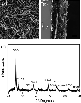 | ||
| Fig. 1 (a) and (b) Scanning electron microscope images of a cross-linked TiO2 nanowire thin film after thermal annealing: (a) top view (scale bar = 25 μm) and (b) side view from a cross section of the thin film (scale bar = 10 μm). (c) XRD pattern of the TiO2 nanowires showing a mixture of anatase (A) and rutile (R) phases. | ||
As synthesized, TiO2 nanowires have very low intrinsic conductivity. To increase their conductivity, the nanowires were annealed in a reducing environment at elevated temperature to create oxygen vacancies.27 When oxygen atoms leave the lattice, Ti4+ ions are reduced to Ti3+, which act as electron donors to the conduction band of TiO2. This n-type doping process increases the conductivity of the material by several orders of magnitude. Single nanowire I–V measurements indicate that the conductivity of an n-doped nanowire is around 10 Ω−1m−1. Comparison of the XRD patterns before and after the process confirms that annealing does not change the lattice structure of the nanowires.
Water photolysis
Fig. 2(a) shows current-potential curves for a 22-μm thick TiO2 nanowire thin film in the dark and under simulated AM 1.5 G illumination. The electrolyte was a 1.0M NaOH aqueous solution (pH = 13.8 at 25 °C).28 No significant dark anodic current is observed until the potential of the working electrode reaches 0.6 VAgCl/Ag. The thermodynamic potential threshold for oxygen evolution, E![[circle, cut, short horiz bar]](https://www.rsc.org/images/entities/char_e0eb.gif) (O2/H2O), is determined by the Nernst equation:
(O2/H2O), is determined by the Nernst equation: | (1) |
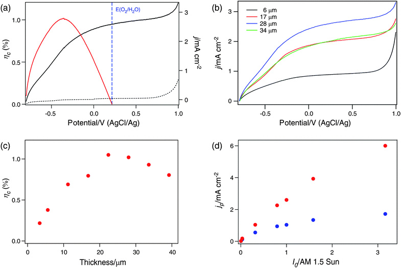 | ||
| Fig. 2 (a) Current density (j)-potential curves in the dark (dashed black line) and in simulated AM 1.5 illumination (solid black line) for a 22-μm TiO2 nanowire thin film. The photoconversion efficiency (ηc) calculated from eqn (2) is shown in solid red. The thermodynamic potential threshold for oxygen evolution is labeled by the vertical blue line. (b) Current density (j)-potential curves in simulated AM 1.5 illumination for TiO2 nanowire thin films with different thicknesses. (c) Thickness dependence for the maximum photoconversion efficiencies of TiO2 nanowire thin films. (d) Power dependence of the photocurrent density (jp) at the thermodynamic potential threshold for oxygen evolution in 1 M NaOH (red dots) and in 10 mM NaOH (blue dots) electrolytes. | ||
This threshold sets the upper limit for the working electrode potential under which the photoelectrochemical cell has a net gain of free energy from the light. Under AM 1.5 illumination, photocurrent is generated at working electrode potentials as low as −0.8 VAgCl/Ag, giving the flat band potential (Efb) at the TiO2/electrolyte contact.29 The photocurrent rises as the anode potential increases, reflecting increased charge carrier separation efficiency. It reaches 2.6 mA cm−2 at E(O2/H2O), which is roughly twice as much as the photocurrent observed for TiO2 nanotube arrays under the same conditions.5
The energy conversion efficiency of the photoelectrochemical cell can be calculated as follows:26
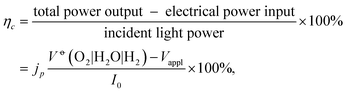 | (2) |
(O2|H2O|H2) = 1.228 V is the chemical energy harvested by converting H2O to H2 and O2, Vappl is the external voltage applied to the cell, and I0 = 100 mW cm−2 is the AM 1.5 G incident light power. We calculate the external voltage with the assumption that the counter electrode has no overpotential. The potential of an ideal counter electrode (cathode) is explicitly defined by the H2O/H2 pair, which can be derived from the Nernst relation. The applied voltage is then given by Vappl = Eanode – Ecathode = Eanode – E(H2O/H2), where E(H2O/H2) = −0.817 VNHE = −1.013 VAgCl/Ag in a 1.0 M NaOH solution. We note that the definition of external voltage has previously been a source of confusion in the field, as most electrochemical measurements are performed in a three-electrode system that does not have a fixed counter electrode (cathode) potential.30 When the applied voltage is defined instead as |Eanode − Eoc|, where Eanode is the working electrode potential and Eoc is the open circuit potential, the efficiency can be overestimated.30
Fig. 2(a) shows the values of ηc measured from our devices. The maximum ηc is measured to be 1.05% at −0.41 VAgCl/Ag, the largest efficiency that has ever been reported for TiO2 photoelectrolysis under AM 1.5 G simulated light. Fig. 2(b) shows the current-potential curves for TiO2 nanowire thin films with thicknesses ranging from 3 μm to 40 μm. The films were mechanically stable in the aqueous electrolyte after chemical cross-linking and annealing. Some nanowires (5∼10%) were found to detach from the thicker films (>30 μm) after a few rounds of measurements, and consequently the electrochemical data shown here were collected from the first couple of measurements. The curves have similar shape and identical photocurrent onset potential. At potentials higher than 0.8 V, thinner films show higher dark current, which is due to the exposure of the back contact metal (Ti/Pt) to the electrolyte solution. The maximum ηc increases monotonically until the film thickness reaches 22 μm, but bends over toward a flatter curve as the thickness increases further (Fig. 2(c)). This dependence is markedly different from previous studies of photocurrent dependence on film thickness in compact thin films.7 The value of ηc decreases for thicker films, most likely due to the increase of the majority carrier path length to the back contact.
The high photocurrent and ηc values observed in our devices result from the large surface area of the cross-linked nanowire geometry. Once a photon is absorbed, the photogenerated minority carriers (holes) have a short distance to travel to reach the water/TiO2 interface. By contrast, in compact thin films, the distance that the minority carrier needs to travel increases with the film thickness, thereby leading to a tradeoff between carrier recombination and optical density. Furthermore, in our network geometry, the voids in the TiO2 nanowire thin film are large (∼2 μm) and well connected, allowing the electrolyte to diffuse freely and reducing the anode polarization caused by the consumption of OH−:
| 4 OH− → O2 + 2 H2O + 4 e− |
The diffusion of electrolyte through the network explains why the energy conversion efficiency is higher than the previously studied anodized TiO2 nanotube array, which also has a large surface-to-volume ratio.9 These arrays have much thinner (∼ 100 nm) and one-dimensional pores with only one open end, hindering ion diffusion. Due to the anode polarization, a higher concentration of OH− is needed to achieve high photocurrent densities and energy conversion efficiencies. Fig. 2(d), which shows the dependence of the photocurrent as a function of the illumination intensity, demonstrates this effect. Here, the anode potential was fixed at the thermodynamic threshold for oxygen evolution (0.216 VAgCl/Ag for 1 M NaOH and 0.323 VAgCl/Ag for 10 mM NaOH). In the 1 M NaOH solution, the photocurrent is proportional to the incident intensity until it rises above 1 Sun at AM 1.5, at which point the photocurrent starts to saturate. The saturation behavior is more pronounced in a 10 mM NaOH solution due to limited mass transport of OH− in the dilute solution. Compensating the lower ionic concentration of 10 mM NaOH with an inert electrolyte such as Na2SO4 slightly increases the photocurrent, but does not affect the saturation behavior (see ESI†). We note that oxygen bubbles on the anode may also contribute to the decrease in efficiency at higher photocurrent density because they can obstruct the optical path.
Spectral dependence of photoelectrolysis
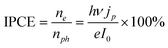
The photocurrent action spectrum is shown in Fig. 3 by plotting IPCE against the excitation wavelengths. IPCE, defined as the number of photogenerated electrons (ne) divided by the number of incident photons (nph), is given by the equationwhere jp is the photocurrent density, ν and I0 are respectively the frequency and the power density of the incident light, h is the Planck constant, and e is the elementary charge. As is clearly seen, an IPCE of up to 90% was achieved at 350 nm excitation. The IPCE does not drop to zero when the incident photon energy falls below the band gap (3.0 eV, 410 nm). It is as high as 1% for 420 nm, and remains about 0.1% in the range of 430–480 nm. Though much less significant for longer wavelengths (λ > 500 nm), the photocurrent is still above the detection limit of our potentiostat. To confirm that our devices' response to visible light is not due to UV light that leaked through our filters, we inserted an additional 400 nm or 420 nm longpass filter (OD ≥ 2 for UV) into the light path. The photocurrent response to visible light was unaffected, confirming our visible light photocurrent measurements.
 | ||
| Fig. 3 (a) IPCE at various excitation wavelengths. Inset: diagram showing a proposed mechanism for the photocurrent observed under the visible light, which involves the excitation of electrons trapped in surface states. (b) UV-Vis diffuse reflectance of a TiO2 nanowire thin film before (blue) and after (red) thermal annealing. | ||
Sub-band gap optical absorption in the thermally annealed TiO2 nanowires is confirmed by diffuse reflectance spectroscopy (Fig. 3(b)). Before thermal annealing, the TiO2 nanowires showed strong optical absorption in the UV but high and uniform reflectance in the visible range, consistent with its snow white appearance. After thermal annealing the reflectivity in the visible range was significantly reduced, signifying sub-band gap absorption. We note that increased optical absorption at longer wavelengths does not generate larger photocurrent, thereby ruling out the possibility that the photocurrent in the visible range is due to a thermal effect.
TiO2 that is heavily doped by carbon or nitrogen can have a significantly red-shifted band edge;31,32 however, our TiO2 is not doped by other elements, as confirmed by the energy dispersive X-ray spectroscopy (EDS: see ESI†). It has been previously reported that n-type TiO2 has localized defect states due to oxygen vacancies in its lattice.33 These oxygen vacancies arise when an oxygen anion (O2−) is replaced by an electron pair. A large fraction of the doped electrons do not ionize to the conduction band, but form localized states, giving rise to optical absorption in the visible spectrum. In our system, after the TiO2 nanowires are thermally annealed, most of these oxygen vacancy defect states should remain near the surface. The inset of Fig. 3 depicts a proposed mechanism for the photoelectrochemistry catalyzed by such defect states. In this mechanism, an electron is optically excited from the surface states to the conduction band, leaving a localized hole that may oxidize the O2/H2O pair if it is at a higher potential than E(O2/H2O).
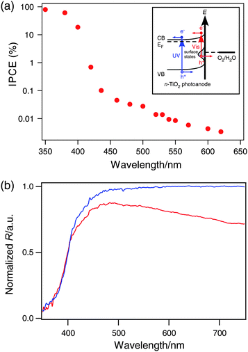
In order to further investigate the nature of the sub-band gap absorption, we performed single nanowire scanning photocurrent measurements. The single TiO2 nanowire device was located from the optical reflection image (Fig. 4(a)) before the photocurrent scan. Both the optical reflection and photocurrent images are diffraction-limited, which sets the resolution of our measurements at 200–300 nm. The excitation wavelength was tuned over a range of 480–700 nm, which is below the band gap of TiO2. Two photocurrent spots of opposite sign are seen in the photocurrent image (Fig. 4(b)) at the two electrical contacts. The photocurrent is on the order of 10 pA at an excitation power of around 1 μW. The sign of the photocurrent indicates that the current is flowing from the TiO2 nanowire to the Ti contact for both contacts, consistent with an n-type Schottky barrier. The magnitude of the photocurrent is proportional to the intensity of the excitation laser (Fig. 4(c), inset), signifying that single-photon absorption is responsible for the observed photocurrent. The photocurrent thus provides evidence for the optical excitation of occupied surface trap states. The band alignment and the photocurrent generation mechanism are shown in the inset of Fig. 4(c). The integrated photocurrent at each contact was normalized by the power of the excitation laser, and plotted against the excitation wavelength in Fig. 4(c). It is clear that a higher quantum efficiency is achieved for shorter wavelengths, which is the same behavior seen in the photoelectrochemistry measurements.
 | ||
| Fig. 4 (a) Optical reflection and (b) scanning photocurrent image recorded from a single TiO2 nanowire with a 600 nm incident laser. Scale bars = 1 μm. (c) The wavelength dependence of the photocurrent (Ip) excited near the two contacts. Insets: (left bottom) power (Pinc) dependence of the photocurrent excited at 600 nm and (right top) a proposed mechanism for the photocurrent. | ||
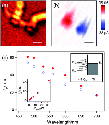
The wavelength dependence of the photocurrent-voltage curves is shown in Fig. 5(a) for a few selected wavelengths. From these curves the open-circuit potential Eoc at each excitation wavelength (Fig. 5(b)) can be measured, allowing the determination of the photovoltage, Vph = Eoc – EF,![[thin space (1/6-em)]](https://www.rsc.org/images/entities/char_2009.gif) electrolyte.34 Here, EF,electrolyte represents the initial Fermi level of the electrolyte, which can be anywhere between E(O2/H2O) and E(H2O/H2), depending on the initial relative concentrations of O2 and H2 in the cell.35 In our setup, EF,electrolyte is measured to be around −0.15 VAgCl/Ag.
electrolyte.34 Here, EF,electrolyte represents the initial Fermi level of the electrolyte, which can be anywhere between E(O2/H2O) and E(H2O/H2), depending on the initial relative concentrations of O2 and H2 in the cell.35 In our setup, EF,electrolyte is measured to be around −0.15 VAgCl/Ag.
 | ||
| Fig. 5 Current-potential curves for different excitation wavelengths: 400 nm, 420 nm, 480 nm, and 570 nm. (b) Open circuit (photocurrent onset) potential (Voc) vs. incident photon energy. The dotted blue line denotes the initial Fermi level of the electrolyte solution. Insets: diagrams showing the band alignment at open circuit potentials for excitations above (left) and below (right) the band gap. ηa is the anode overpotential for oxygen evolution. | ||
In the photovoltage spectrum, there are two different behaviors above and below the band gap. Above the band gap, the photovoltage is almost independent of the incident wavelength. Hot carriers generated above the band gap thermalize quickly to the band edge, and the photocurrent onset potential is solely determined by the flat band potential of TiO2 (Fig. 5(b), left inset). The photovoltage is independent of the incident light intensity in the experimental range (10−3 ∼ 1 mW cm−2), consistent with earlier reports.35,36 As the incident photon energy falls below the band gap of TiO2 (3.0 eV, 410 nm), a sudden decrease (∼ 0.4 V) of the photovoltage occurs. Below the band gap, the open circuit potential gradually approaches the initial Fermi level of the electrolyte, and the photovoltage approaches zero. Under visible light, electrons from surface trap states can be excited and form a quasi-Fermi level of holes (EF*), which is much shallower due to the much lower density of states.37 In this case, the photocurrent onset is only reachable with a band bending (Fig. 5(b), right inset), which leads to the sudden drop of photovoltage from 400 nm to 420 nm. At longer wavelengths of excitation, the photoexcited surface states become less energetic, and the deep trap states are highly localized, contributing less to the quasi-Fermi level. The quasi-Fermi level of holes approaches the electron Fermi level (EF), and the photovoltage eventually approaches zero.
Surface plasmon enhanced visible light photocurrent
We also investigated the plasmonic enhancement of photocurrent by adding metallic nanoparticles to the nanowire thin films (Fig. 6(a)). TiO2 nanowire thin films coated with gold or silver were prepared as described in the experimental section. After thermal annealing, the thin metal layer broke into nanoparticles that covered the TiO2 nanowires uniformly (Fig. 6(a), insets). This surface coating led to an enhancement of visible light photocurrent of up to a factor of 10 (Fig. 6(b)). The maximum enhancement occurs around 600 nm, which corresponds to the plasmon resonance of these metal nanoparticles within TiO2.38,39 Above the band gap, no enhancement was observed because the interband transitions of gold or silver dampen the surface plasmon mode in the UV range.40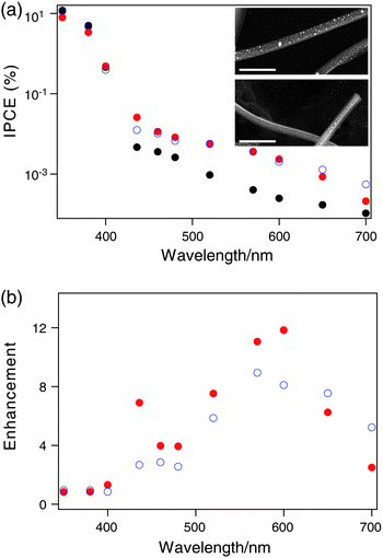 | ||
| Fig. 6 (a) The wavelength dependence of IPCE for sparse films of TiO2 nanowires (black dots), coated with silver nanoparticles (blue circles), and coated with gold nanoparticles (red dots). Inset: the SEM images of the TiO2 nanowires coated with silver nanoparticles (top) and gold nanoparticles (bottom). Scale bars = 1 μm. (b) The enhancement of IPCE versus wavelength by silver nanoparticles (blue circles) and gold nanoparticles (red dots). | ||
It should be noted that the enhancement of photocurrent was observed only for very thin nanowire films (≤ 1 μm). No enhancement was seen for thicker films despite a homogeneous coating of metal nanoparticles in the multi-layer nanowire film (nanoparticle deposition was performed after each nanowire layer deposition). This observation indicates that the enhancement is due to the far-field scattering of the incident photon by the metal nanoparticles that increases the effective optical path length. As the TiO2 nanowire film gets thicker, incident photons can scatter multiple times off the nanowires, leading to a long effective path length even in the absence of metal nanoparticles. We note that the absence of enhancement in thicker films suggests that local electric field enhancement does not play a significant role in these devices. We note that the use of plasmonic metal nanoparticles to increase optical absorption in very thin slabs of semiconductor materials has also been explored in photovoltaic devices and various photocatalytic systems.41–43 Because of the relatively small degree of absorption in the visible for these nanowires, the plasmon-enhanced photocurrent does not contribute significantly to the overall device efficiency. This strategy, however, might be more effective in other material systems with higher visible absorption, such as doped TiO2 or other materials.
Conclusions
Efficient water splitting using sunlight has long been an intensely pursued goal in chemistry, and may eventually provide a viable pathway towards alternative energy sources. In this report, we have demonstrated that the high surface area architecture of the cross-linked TiO2 nanowires leads to highly efficient photoelectrochemical splitting of water. Specifically, the geometry of the nanowire network achieves large surface area without sacrificing electrical conductivity, and allows for electrolyte diffusion through the interconnected voids, giving the highest solar energy conversion efficiency reported for water photolysis with TiO2 photoanodes. This strategy should be applicable for other material systems as well, and may significantly enhance the performance of devices incorporating lower band gap materials, which generally have short minority carrier diffusion lengths.21,44 We observed plasmon enhancement of visible light absorption in thin nanowire films (<1 μm thickness), where the far-field optical scattering of the metal nanoparticles increases the optical path of the incident light in the plane of the thin film. These characteristics could be used as general design principles for other photoelectrochemical systems, including dye-sensitized solar cells.Acknowledgements
We are grateful to Prof. Eric Mazur and Mark Winkler for the use of their AM 1.5 G solar simulator. We also thank Dr Jin-Seok Lee for his help in the synthesis of the nanowires and Dr Abram Falk for helpful discussions. The work is supported by the NSF. N. Snapp also acknowledges the NSF and NDSEG fellowship programs for support.Notes and references
- A. Fujishima and K. Honda, Nature, 1972, 238, 37–38 CAS.
- T. G. Deutsch, C. A. Koval and J. A. Turner, J. Phys. Chem. B, 2006, 110, 25297–25307 CrossRef CAS.
- J. F. Reber and M. Rusek, J. Phys. Chem., 1986, 90, 824–834 CrossRef CAS.
- A. B. Murphy, P. R. F. Barnes, L. K. Randeniya, I. C. Plumb, I. E. Grey, M. D. Horne and J. A. Glasscock, Int. J. Hydrogen Energy, 2006, 31, 1999–2017 CrossRef CAS.
- C. M. Ruan, M. Paulose, O. K. Varghese, G. K. Mor and C. A. Grimes, J. Phys. Chem. B, 2005, 109, 15754–15759 CrossRef CAS.
- H. Tang, K. Prasad, R. Sanjines, P. E. Schmid and F. Levy, J. Appl. Phys., 1994, 75, 2042–2047 CrossRef CAS.
- M. Takahashi, K. Tsukigi, T. Uchino and T. Yoko, Thin Solid Films, 2001, 388, 231–236 CrossRef CAS.
- A. K. Ghosh and H. P. Maruska, J. Electrochem. Soc., 1977, 124, 1516–1522 CrossRef CAS.
- G. K. Mor, K. Shankar, M. Paulose, O. K. Varghese and C. A. Grimes, Nano Lett., 2005, 5, 191–195 CrossRef CAS.
- J. Tang, Y. Y. Wu, E. W. McFarland and G. D. Stucky, Chem. Commun., 2004, 1670–1671 RSC.
- B. Guo, Z. L. Liu, L. Hong, H. X. Jiang and J. Y. Lee, Thin Solid Films, 2005, 479, 310–315 CrossRef CAS.
- O. K. Varghese, M. Paulose, K. Shankar, G. K. Mor and C. A. Grimes, J. Nanosci. Nanotechnol., 2005, 5, 1158–1165 CrossRef CAS.
- O. K. Varghese, D. W. Gong, M. Paulose, C. A. Grimes and E. C. Dickey, J. Mater. Res., 2003, 18, 156–165 CrossRef CAS.
- G. Mie, Ann. Phys., 1908, 25, 377–445 CAS.
- C. F. Bohren and D. R. Huffman, Absorption and scattering of light by small particles, Wiley, New York, 1983 Search PubMed.
- A. Hartstein, J. R. Kirtley and J. C. Tsang, Phys. Rev. Lett., 1980, 45, 201–204 CrossRef CAS.
- J. Gersten and A. Nitzan, J. Chem. Phys., 1981, 75, 1139–1152 CrossRef CAS.
- D. M. Schaadt, B. Feng and E. T. Yu, Appl. Phys. Lett., 2005, 86, 063106 CrossRef.
- S. Pillai, K. R. Catchpole, T. Trupke and M. A. Green, J. Appl. Phys., 2007, 101, 093105 CrossRef.
- S. S. Kim, S. I. Na, J. Jo, D. Y. Kim and Y. C. Nah, Appl. Phys. Lett., 2008, 93, 073307 CrossRef.
- A. Kay, I. Cesar and M. Gratzel, J. Am. Chem. Soc., 2006, 128, 15714–15721 CrossRef CAS.
- O. K. Varghese, D. W. Gong, M. Paulose, K. G. Ong, E. C. Dickey and C. A. Grimes, Adv. Mater., 2003, 15, 624–627 CrossRef.
- X. C. Jiang, Y. L. Wang, T. Herricks and Y. N. Xia, J. Mater. Chem., 2004, 14, 695–703 RSC.
- Y. L. Wang, X. C. Jiang and Y. N. Xia, J. Am. Chem. Soc., 2003, 125, 16176–16177 CrossRef CAS.
- A. L. Linsebigler, G. Q. Lu and J. T. Yates, Chem. Rev., 1995, 95, 735–758 CrossRef CAS.
- K. Shankar, J. I. Basham, N. K. Allam, O. K. Varghese, G. K. Mor, X. J. Feng, M. Paulose, J. A. Seabold, K. S. Choi and C. A. Grimes, J. Phys. Chem. C, 2009, 113, 6327–6359 CrossRef CAS.
- D. C. Cronemeyer, Phys. Rev., 1952, 87, 876–886 CrossRef CAS.
- D. R. Lide, CRC handbook of chemistry and physics, CRC Press, 2008 Search PubMed.
- A. J. Bard and L. R. Faulkner, Electrochemical methods: fundamentals and applications, Wiley, New York, 2001 Search PubMed.
- C. A. Grimes, O. K. Varghese and S. Ranjan, Light, water, hydrogen: the solar generation of hydrogen by water photoelectrolysis, Springer, New York, 2008 Search PubMed.
- S. U. M. Khan, M. Al-Shahry and W. B. Ingler, Science, 2002, 297, 2243–2245 CrossRef CAS.
- R. Asahi, T. Morikawa, T. Ohwaki, K. Aoki and Y. Taga, Science, 2001, 293, 269–271 CrossRef CAS.
- D. C. Cronemeyer, Phys. Rev., 1959, 113, 1222–1226 CrossRef CAS.
- P. Blood, Semicond. Sci. Technol., 1986, 1, 7–27 CrossRef CAS.
- A. J. Nozik, Annu. Rev. Phys. Chem., 1978, 29, 189–222 CAS.
- A. B. Bocarsly, J. M. Bolts, P. G. Cummins and M. S. Wrighton, Appl. Phys. Lett., 1977, 31, 568–570 CrossRef CAS.
- H. Gerischer, J. Electroanal. Chem., 1977, 82, 133–143 CrossRef CAS.
- J. J. Mock, D. R. Smith and S. Schultz, Nano Lett., 2003, 3, 485–491 CrossRef CAS.
- J. N. Anker, W. P. Hall, O. Lyandres, N. C. Shah, J. Zhao and R. P. Van Duyne, Nat. Mater., 2008, 7, 442–453 CrossRef CAS.
- P. B. Johnson and R. W. Christy, Phys. Rev. B: Solid State, 1972, 6, 4370–4379 CrossRef CAS.
- H. A. Atwater and A. Polman, Nat. Mater., 2010, 9, 205–213 CrossRef CAS.
- K. Awazu, M. Fujimaki, C. Rockstuhl, J. Tominaga, H. Murakami, Y. Ohki, N. Yoshida and T. Watanabe, J. Am. Chem. Soc., 2008, 130, 1676–1680 CrossRef CAS.
- S. D. Standridge, G. C. Schatz and J. T. Hupp, J. Am. Chem. Soc., 2009, 131, 8407–8409 CrossRef CAS.
- I. Cesar, A. Kay, J. A. G. Martinez and M. Gratzel, J. Am. Chem. Soc., 2006, 128, 4582–4583 CrossRef CAS.
Footnotes |
| † Electronic supplementary information (ESI) available: Energy dispersive X-ray spectroscopy, water photolysis and diffuse reflectance experimental details. See DOI: 10.1039/c0sc00321b |
| ‡ These two authors contributed equally to this work. |
| This journal is © The Royal Society of Chemistry 2011 |