Synthesis and application of core-shell Au–TiO2 nanowire photoanode materials for dye sensitized solar cells†
Gayatri
Sahu
,
Scott W.
Gordon
and
Matthew A.
Tarr
*
Department of Chemistry and Advanced Materials Research Institute, University of New Orleans, New Orleans, LA 70148, USA. E-mail: mtarr@uno.edu; Fax: 1-504-280-6860; Tel: 1-504-280-6323
First published on 18th November 2011
Abstract
Dye sensitized solar cells (DSSCs) have been widely studied as alternatives for generation of electricity from sunlight due to their efficiency and cost effectiveness. Increasing the electron transport out of the metal oxide is important in achieving higher efficiency. Enhancing light absorption can also improve cell efficiency. The motive of this work was to synthesize and use Au–TiO2 core-shell nanowires as anode materials in DSSCs in order to increase cell efficiency by enhancing electron transport out of the oxide and/or increasing light collection efficiency. TiO2 nanotubes were first grown in alumina templates using a sol–gel method. Gold nanowires were subsequently grown in the pores of these tubes by electrodeposition. Resulting nano-structured arrays were characterized using electron microscopy and diffraction techniques; the results show that the wires were highly aligned and well separated. The current–voltage (J–V) behavior for the Au–TiO2 core-shell nanowire based DSSCs was compared to the J–V data for TiO2 nanotube based DSSCs, indicating substantial improvements upon incorporation of the Au core nanowires. TiCl4 treatment of the Au–TiO2 core-shell nanowire structures resulted in further efficiency improvements.
Introduction
Highly efficient and low cost conversion of solar energy to electricity remains a challenge even after many years of research. Dye sensitized solar cells (DSSCs) offer the potential for low cost cells, but efficiency has not improved beyond a maximum of 11% achieved around 1990.1–2 The breakthrough of dye sensitized devices as solar cells was based on some innovative points, such as mesoporous semiconductors of high surface area which allowed high density of dye adsorption. Furthermore, development of stable organometallic sensitizers bearing attachment groups which bind strongly with the semiconductor led to enhanced charge injection efficiency. Based on these features, overall efficiencies of over 10% were obtained by O'Regan and Grätzel in 1991 for dye sensitized mesoporous TiO2 electrodes in contact with an electrolyte containing an iodide/triiodide based redox couple for dye regeneration.1–2 Even though the nanoparticle films provide high surface area for dye adsorption, the electron transport rate through the oxide is comparatively slow because of low electron diffusion in the polycrystalline oxide. The slow diffusion is caused by multiple trapping and de-trapping events occurring in the porous semiconductor grain boundaries of the TiO2 nanoparticles.3Electron transport in mesoscopic thin films is vulnerable to recombination losses at the particle–solution interface. Consequently, high interface recombination reaction rates limit the device efficiency. To resolve these problems, a DSSC based on an array of one-dimensional ZnO nanostructures was first introduced by Law et al. in 2005.4 Unfortunately, the ZnO photoanodes consistently showed lower performance due to their instability in acidic dye media5 and lower roughness factor (<200).4 TiO2, a more stable semiconductor material, was subsequently synthesized as nanorod arrays.6–12 Fujihara et al. have achieved TiO2 nanorod arrays on fluorine doped tin oxide glasses using a method called spray deposition.6 The XRD pattern of the sintered TiO2 nanorods revealed that the phase corresponded to anatase. Photovoltaic measurements were taken with these TiO2 nanorod arrays as photoanodes under 1 sun (AM 1.5). power conversion efficiency (η) of 5.8%, a current density (Jsc) of ∼13.7 mA cm−2, an open circuit voltage (Voc) of ∼0.8 V, and a fill factor (FF) of ∼51%. However the nanorods showed comparatively low surface area. To overcome the limitations of lower nanorod array surface area, TiO2 nanotubes were prepared by several methods and have been applied in DSSCs as photoanode materials.13–18 The nanotube photoanodes were much more efficient at light harvesting due to the large nanocrystallite surface area available for dye adsorption. Also, the nanotubes provided an easier pathway to capture photogenerated charges and transport them to the conducting electrode surface.19 However, the need for decreasing the recombination of electrons and holes after band gap excitation was not fulfilled due to the bulk defects and grain boundaries which are major causes of limited photoconversion efficiency. There is a report which focuses on using nanoparticle decorated ZnO–TiO2 core-shell nanorod arrays,20 and the use of two different wide band gap semiconductors as anodes in DSSC has also been reported.19,21–24
Three dimensional core-shell structures having TiO2 as shell and various guest metal/metal oxide as core via electrodeposition have been reported.25–30 Others have reported metal doped TiO2 nanobelts31 and have discussed the possibility of using the synthesized structures as photoanodes in photovoltaic devices but did not actually do so. The overall goal of the current research was to enhance the efficiency of DSSCs and practically achieve efficiency nearer to the theoretically expected value.32–33 Since one of the major problems in achieving high efficiency is poor electron transport, we have synthesized Au–TiO2 core-shell nanowires to overcome this barrier. There are reports which have synthesized various metal nanoparticles or nanorods embedded in TiO2 nanotubes.34–37 We have applied a novel technology to fabricate TiO2 nanostructures with core Au nanorods, keeping a large TiO2 surface area available for dye adsorption. We adopted a template based method for preparing these nanostructures because there are a number of useful features associated with this method. For example, it allows flexibility in tuning the length and diameter of the tubes. Furthermore, it allows varying the nanotube shell thickness by controlling the synthesis parameters. There are several types of membranes which have been used as templates for nanostructures synthesis. Most of the work has been done with porous alumina membranes (also known as anodic aluminum oxide, AAO) and track-etch polymeric membranes made of polycarbonate. We have used the AAO membranes to synthesize our photoanode materials. After synthesis, the desired nanoarchitectures were characterized using different probe techniques such as field emission scanning electron microscopy (FESEM), energy dispersive spectroscopy (EDS), transmission electron microscopy (TEM) and X-ray powder diffraction (XRD). Using the core-shell nanowire structures as photoanodes, DSSC devices were fabricated and the J–V characteristics were measured.
Experimental
A. Synthesis of TiO2 nanotubes
In this study we used commercial AAO membranes supplied by the Whatman Corp. The average pore diameter and the thickness of the membranes used were 200 nm and 60 μm, respectively. In a typical synthetic process, the 200 nm pore size AAO membrane was masked on one side with transparent tape and then heated to 85 °C for 15 min to remove any atmospheric water in the membrane. A sol–gel precursor solution was prepared by a modified method14 utilizing titanium isopropoxide, Ti(OC3H7)4, mixed with ethanol. The weight ratio of Ti(OC3H7)4![[thin space (1/6-em)]](https://www.rsc.org/images/entities/char_2009.gif) :C2H5OH was 3:1. The membrane was immersed in the precursor solution for 15–35 min (tube length was related to immersion time, supporting information Fig. S1†), then excess liquid was wiped off from the exposed surface of the membrane. This wiping step was necessary in order to avoid an undesirable, thick film of TiO2 on the surface of the AAO membrane which can clog the pores. The template was then left in a covered beaker for 12 h which allowed for the solution to infiltrate the inner walls of the pores of AAO by capillary action, followed by evaporation of the ethanol and hydrolysis of the isopropoxide upon mixing with water from ambient air. Next, the sample was annealed at 500 °C for 30 min in air. The difference in our method compared to the previously reported method14 was that we have used a commercial AAO membrane with openings on both sides allowing us to prepare TiO2 nanotubes open at both ends.
:C2H5OH was 3:1. The membrane was immersed in the precursor solution for 15–35 min (tube length was related to immersion time, supporting information Fig. S1†), then excess liquid was wiped off from the exposed surface of the membrane. This wiping step was necessary in order to avoid an undesirable, thick film of TiO2 on the surface of the AAO membrane which can clog the pores. The template was then left in a covered beaker for 12 h which allowed for the solution to infiltrate the inner walls of the pores of AAO by capillary action, followed by evaporation of the ethanol and hydrolysis of the isopropoxide upon mixing with water from ambient air. Next, the sample was annealed at 500 °C for 30 min in air. The difference in our method compared to the previously reported method14 was that we have used a commercial AAO membrane with openings on both sides allowing us to prepare TiO2 nanotubes open at both ends.
B. Synthesis of Au–TiO2 core-shell nanowires
After the TiO2 nanotubes were obtained with the desired morphology and crystalline anatase phase, bottom up constant current electrodeposition was carried out in order to grow Au–TiO2 core-shell nanowires. In order to grow the Au nanowires inside the hollow channels of the TiO2 nanotubes while still embedded in the AAO membranes, a silver film was first sputtered on the back of the template (the side containing the TiO2 nanotubes). The Ag backed AAO template with TiO2 nanotubes served as the working electrode (cathode), a Pt wire served as anode, and Ag/AgCl was used as the reference electrode. The gold plating solution (Orotemp 24) was purchased from Technic, Inc. The silver side of the template was attached to copper tape (3M), and the opposite side of the copper tape was covered with its original polymer backing as well as 3M Scotch tape so that electrodeposition could only occur through the open pores of the TiO2 tubes within the AAO membrane. Electrodeposition was carried out at room temperature using constant current with a single channel potentiostat (EG&G Instruments Model 263A). Nanowires were grown into the TiO2 nanotubes with a current of −0.9 mA for up to 80 min. This deposition allowed the wires to grow as far as to the top of the nanotubes, filling the entire channel with Au nanowires. The procedure is illustrated in Fig. 1. After deposition, the sample was rinsed with distilled water, and the AAO containing nanostructure was etched slowly with 3 M NaOH for 30 min. The obtained core-shell nanowires were washed several times with distilled water resulting in well aligned nanowire arrays on a copper substrate. The nanowire arrays were later removed from the copper tape by washing with acetone.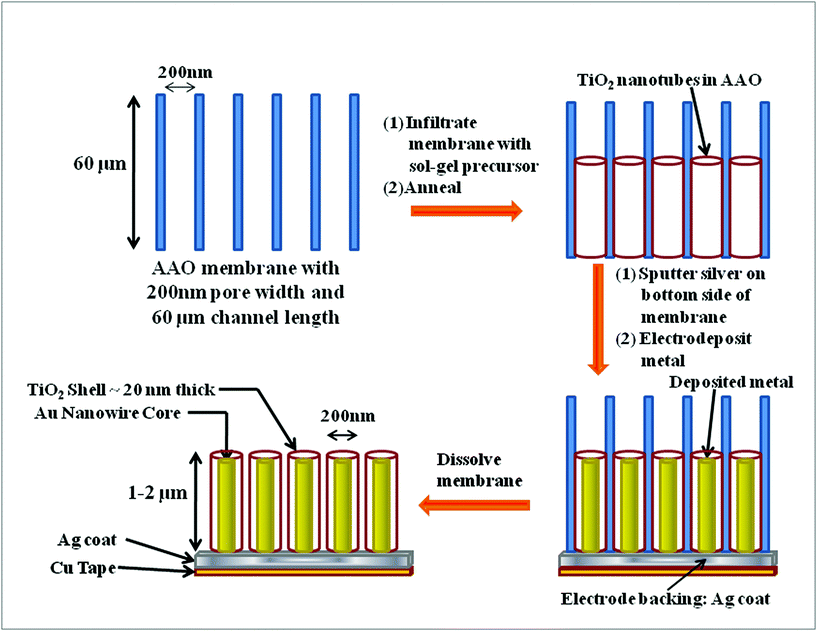
C. Characterization
The structures were characterized by a Carl Zeiss 1530 VP field emission scanning electron microscope (FESEM) and a JEOL 2010 conventional transmission electron microscope (TEM). The compositional analysis was conducted by energy dispersive X-ray spectroscopy (EDS). For FESEM observation, TiO2 nanotube samples were attached to a glass substrate using epoxy glue. The AAO template was removed using aqueous 3 M NaOH for 45 min. The sample was observed by FESEM and XRD after drying overnight. The X-ray diffraction (XRD) patterns of samples were collected by a Philips X-pert PW 3040 MPD X-ray powder diffractometer operated at 40 kV and 40 mA current with Cu-Kα radiation.D. Solar cell fabrication and characterization
Photoanodes utilizing TiO2 nanotubes and Au–TiO2 nanowires were prepared by transferring the nanostructures onto a fluorine doped tin oxide (FTO) glass substrate obtained from Solaronix (TCO10-10, sheet resistance 10 Ω sq−1) using a modified method.14 First method involves depositing a thin layer (∼2 μm) of nanocrystalline TiO2 paste (Aldrich) onto the FTO conducting surface in order to promote adhesion of the nanostructures and also to prevent electrical shorting with the redox electrolyte coming into direct contact with the FTO layer. The AAO containing the TiO2 nanotubes or Au–TiO2 nanowires was attached to an adhesive transparent tape with the silver sputtered side of the AAO template (in case of Au–TiO2 nanowires) attached to the adhesive side of the tape. The AAO was dissolved away using 3 M NaOH for 45 min. This assembly, tape side up, was then applied to the TiO2 coated FTO substrate, The tape was then peeled off and the remaining structure was heated to 450 °C for 30 min.14 When the tape was removed, the thin layer of silver was peeled off along with the tape and was no longer visible after the tape was removed (see Fig. S2 in supporting information†). In the second method, the AAO containing TiO2 nanotubes or Au–TiO2 nanowires were dissolved in 3 M NaOH which resulted in free arrays of TiO2 nanotubes or Au–TiO2 core-shell nanowires in NaOH solution. The arrays of nanotubes or Au–TiO2 nanowires were washed with DI H2O four times in order to remove the residual NaOH. The nanostructures were then washed with ethanol to remove residual water. The freely suspended nanostructure arrays were then transferred and adhered onto a pre-cleaned FTO slide followed by annealing in air at 450 °C for 30 min. This second method was applied in order to assess the effect of the nanocrystalline TiO2 paste on the performance of the device. The resulting TiO2 nanotube or Au–TiO2 core-shell nanowire film on the FTO was sensitized for 24 h by soaking in dye solution overnight. A ruthenium dye (N-535, Solaronix) was prepared by dissolving 25 mg of the solid in 1 mL of ethanol. A platinum coated FTO counter electrode was prepared by brushing with a thin layer of Platisol T (Solaronix). The I−/I3− electrolyte was prepared using 0.6 M 1-methyl-3-propylimidazolium iodide, 0.05 M iodine, 0.05 M LiI and 0.5 M tert-butylpyridine in 25 mL acetonitrile:valeronitrile (1:1 volume ratio). Two small holes were drilled in the glass of the platinum electrode in order to later inject the electrolyte. The two electrodes were tightly sandwiched together by using Surlyn® sealant (Solaronix), and the sandwiched electrodes were sealed by heating for 5 min with a heat gun. The electrolyte was carefully introduced into the space between the two electrodes through one hole on the Pt electrode with a syringe. The drilled holes were then sealed. The details of the processes for transferring the nanostructures onto FTO using the first and second method and device fabrication has been given in Fig. S3 in supporting information.† Photovoltaic data were measured using an ATLAS Suntest (CPS+) solar simulator set at 100 mW cm−2 full spectrum power (equivalent to AM-1.5). J–V data were generated using a Keithley 2400 source meter. The light intensity of the xenon light source was adjusted by using an NREL calibrated silicon photodiode (Hamamatsu S1787-08 for visible to IR range). The incident photon to current efficiency (IPCE) was measured using a modified fluorescence spectrometer (PTI). In detail, a 75 watt xenon lamp was coupled to a monochromator with a computer controlled stepper motor (Superior Electric MO61-CS02). The intensity of incident light at each wavelength was measured by a calibrated silicon photodiode (Newport 818-UV-L) and the photoresponse of the test cell was subsequently measured under identical conditions.
E. TiCl4 Treatment
Surface treatment of the TiO2 photoanodes with a TiO2 precursor such as titanium tetrachloride TiCl438–42 and titanium isopropoxide Ti(OC3H7)443 has already been proven to enhance solar cell device performance by increasing photocurrent,44 enhancing surface area,45 improving electron transport,38 and improving anchoring of the dye.41 In order to passivate gold exposed at the ends of our Au–TiO2 nanowires, the Au–TiO2 nanowire film on FTO was also subjected to 0.1 M TiCl4 (Aldrich) aqueous solution in a closed chamber for 24 h, then washed with distilled water. The electrode was annealed again at 450 °C for 30 min. The color of the electrode was off-white after the TiCl4 treatment. One FESEM image of TiCl4 treated TiO2 nanotube arrays without TiO2 nanoparticle bottom layer has been given in figure S4 in supporting information.† These anodes were treated with ruthenium dye and the DSSC devices were fabricated as described above for TiO2 nanotube cells.F. Dye desorption experiment
The amount of dye adsorbed on the nanostructures was measured by desorbing the dye with 0.2 M NaOH in ethanol. The concentration of desorbed dye was determined by absorbance using a Cary 500 UV-Vis spectrophotometer.Results and discussion
The mechanism for the synthesis of TiO2 nanotubes by sol–gel reaction has been discussed elsewhere.46 The AAO film containing TiO2 nanotubes was heat-treated at 500 °C for 30 min, and the nanotubes obtained were found to be polycrystalline anatase. The XRD pattern (supporting information Fig S5†) showed that the TiO2 nanotubes were highly crystalline anatase. The XRD pattern contained several peaks corresponding to anatase, and the absence of a peak at 27.45° (rutile) suggests that the nanotubes consist predominantly of crystalline anatase TiO2 phase.The FESEM images and the EDS data of synthesized nanotubes are given in Fig. 2, which shows that the synthesized structures were clearly composed of well aligned TiO2 nanotube arrays. The TiO2 nanotubes were around 2–3 μm in length with a ≈300 nm outer diameter. Based on these images, we approximate a tube density of 8 tubes per square micron. Nanotube wall thickness can be varied by varying the immersion time of the AAO membrane into the precursor solution. For example, very thin walled nanotubes were obtained with a short immersion time of 2 min and thick walled nanotubes were obtained with a long immersion time of 10–15 min. The highly magnified thick walled anatase TiO2 nanotubes are shown in Fig. 2a and low magnified side view has been given in Fig. 2b. The nanotubes have a tendency to bundle tightly together due to the surface tension induced by solvent evaporation after the removal of the AAO template. This effect was apparent in all the FESEM images. However, open space is still visible between the tubes.
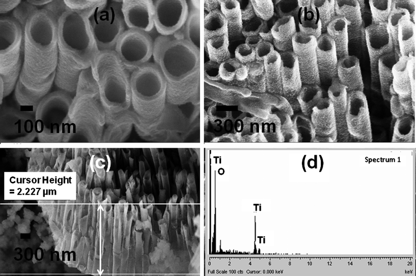 | ||
| Fig. 2 Scanning electron micrographs of (a) top view and (b) side view of thick walled TiO2 nanotubes; length of tubes shown in (c); EDS provided in (d). | ||
To prepare TEM samples, after dissolving the nanotube containing AAO template with 3 M NaOH for 30 min, TiO2 nanotubes in the solvent were carefully removed with a syringe. The sample was then placed in a new glass vial, a few microlitres of toluene were added, and the sample was sonicated for 5 min. This process dispersed the nanotubes without destroying the nanotube structure. TEM images of the TiO2 nanotubes are given in Fig. 3. These images confirm that the average nanotube shell thickness was ∼5–15 nm and the tubes had a diameter of ∼200 nm. The composition of the TiO2 nanotubes was confirmed by EDS analysis, with data shown in Fig. 3c.
 | ||
| Fig. 3 TEM images of sol–gel synthesized TiO2 nanotubes (a, b) and corresponding EDS data (c). | ||
Fig. 4 shows FESEM images of both morphological and compositional data of Au–TiO2 core-shell nanowire arrays on a Cu substrate. Fig. 4a–c show the top views of the Au filled TiO2 nanotubes taken at various magnifications. The images prove the successful growth of the Au–TiO2 core-shell nanoarchitectures. Fig. 4d presents the EDS data for the Au–TiO2 core-shell nanowires, which clearly indicate the presence of Au, Ti, and O.
 | ||
| Fig. 4 FESEM images of Au–TiO2 core-shell nanowires (a–c) and corresponding EDS data (d). | ||
Fig. 5 shows the representative TEM images of the as prepared Au–TiO2 core-shell nanowires. The Au filled TiO2 nanotubes were about 200 nm in diameter. The dark portion inside the shell corresponds to gold, and the gray, polycrystalline regions are the TiO2 shell. It can be clearly seen that the hollow channel of the TiO2 nanotube was entirely filled with gold up to near the tip of the tube. One limitation of this gold filling method is that the metal was polycrystalline in nature, possibly causing poor contact between the oxide and the metal and through the metal core. However, slower electrodeposition might create single crystalline nanowires of gold that would be expected to perform even better for photovoltaic charge transport. We have chosen gold as the material for the metallic core due to its excellent conductivity, inertness, and thermal and chemical stability. Also, metallic nanowires provide enhancement of light absorbance through scattering effects.47 Complete filling of the hollow tube was possible because of the bottom-up electrodeposition method used to fill the TiO2 tubes. The mechanism for the metal growth might be described as follows: The pore bottoms have been made highly conductive by sputtering a thin layer of Ag (< 20 nm), whereas the wall of TiO2 tube has substantial resistance.
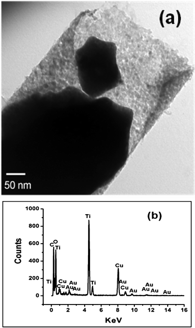 | ||
| Fig. 5 (a) Representative TEM image of the tip of one Au–TiO2 core-shell nanowire and (b) EDS spectrum of the Au–TiO2 nanowires showing the presence of both Au and Ti. | ||
This arrangement allows for uniform pore filling of gold by electrodeposition from pore bottom to the top, resulting in a homogeneous and continuous core-shell nanostructure. The composition of the core-shell nanowire depicted in Fig. 5a was verified by EDS (Fig. 5b). The spectrum indicates that the nanostructure is composed of Au, Ti, and O. The Cu peak comes from the grid.
A schematic of the core-shell nanowire device is given in Fig. 6. Au–TiO2 core-shell nanowires were also used as the photoanode by attaching them to an FTO substrate using the same method described above. Good contact between the gold and the FTO is an important factor in achieving efficient electron transport. Based on FESEM and TEM images, the gold cores come close to the tip of the TiO2 nanotubes and are consequently in close proximity to the TiO2 paste. The synthesized structures served as the photoanode in dye sensitized solar cell devices. Ruthenium dye (N-535) was the sensitizer and I−/I3− served as the redox couple. The J–V characteristics were measured under 100 mW cm−2 simulated sunlight (AM 1.5). We compare the current–voltage characteristics of TiO2 nanotube solar cells with that of Au–TiO2 core-shell nanowires and surface passivated Au–TiO2 core-shell nanowire solar cells. The active area of the anodes for each cell was in the range of 0.12 to 1.04 cm2. The J–V curves obtained are given in Fig. 7. The TiO2 nanotubes had ∼5–15 nm wall thickness, 300 nm outer diameter and 2–3 μm length. The J–V data obtained upon illumination is given in Table 1. The average efficiency and fill factor of two TiO2 nanotube based devices was found to be (0.5 ± 0.2)% and (44 ± 4)%, respectively. When the TiO2 underlayer used for adhesion of the nanowire arrays was tested alone as a DSSC, its efficiency was only 0.35%, indicating that the underlayer did not contribute substantially to the performance of the nanowire devices (Figure S6 in supporting information†).
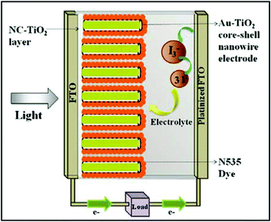 | ||
| Fig. 6 Schematic of assembled TiO2 nanotube DSSC or Au–TiO2 core-shell DSSC (NC = nanocrystalline). Not to scale; tube length exaggerated to better illustrate structure. | ||
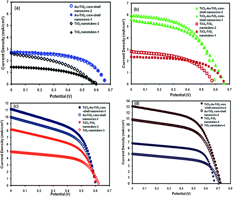 | ||
| Fig. 7 J–V curves for DSSC employing various nanotubes. Panel (a) presents first and second cells made from TiO2 nanotubes (open and closed black diamonds) and first and second cells made from Au–TiO2 core-shell nanowires (open and closed blue circles). Panel (b) presents first and second cells made from TiCl4 treated TiO2 nanotubes (open and closed red squares) and TiCl4 treated Au–TiO2 core-shell nanowires (open and closed green triangles). Panel (c) presents data for cells made from nanostructures without a TiO2 nanoparticle adhesion layer: TiO2 nanotubes (open orange diamonds), TiCl4–TiO2 nanotubes (closed orange diamonds), Au–TiO2 core-shell nanowires (open dark blue circles), and TiCl4–Au–TiO2 core-shell nanowires (closed dark blue circles). Panel (d) presents another set of data for cells made from long (∼6 μm) nanostructures without a TiO2 nanoparticle adhesion layer: TiO2 nanotubes (open purple diamonds), TiCl4–TiO2 nanotubes (closed purple diamonds), Au–TiO2 core-shell nanowires (open brown circles), and TiCl4–Au–TiO2 core-shell nanowires (closed brown circles). Cell efficiencies and other parameters listed in Table 1. | ||
| Photoanode film type | Approx. length (μm) | TiO2 nanoparticle adhesion layer | J sc (mA cm−2) | V oc (V) | FF (%) | η (%) |
|---|---|---|---|---|---|---|
| TiO2 nanotube-1 | 3 | Yes | 1.45 | 0.60 | 46.8 | 0.41 |
| TiO2 nanotube-2 | 2.5 | Yes | 2.62 | 0.59 | 40.8 | 0.63 |
| TiCl4 treated nanotube-1 | 2.5 | Yes | 2.35 | 0.68 | 55.6 | 0.89 |
| TiCl4 treated nanotube-2 | 2.5 | Yes | 2.82 | 0.59 | 49.7 | 0.83 |
| Au–TiO2 core-shell-1 | 3 | Yes | 2.76 | 0.67 | 56.0 | 1.02 |
| Au–TiO2 core-shell-2 | 3 | Yes | 2.69 | 0.69 | 55.0 | 1.04 |
| TiCl4 treated Au–TiO2 core-shell-1 | 3 | Yes | 5.62 | 0.68 | 48.0 | 1.83 |
| TiCl4 treated Au–TiO2 core-shell-2 | 2.5 | Yes | 5.93 | 0.61 | 54.5 | 1.97 |
| TiO2 nanotube-3 | 3 | No | 4.92 | 0.62 | 57.6 | 1.78 |
| TiCl4–TiO2 nanotube-3 | 3 | No | 8.18 | 0.60 | 52.2 | 2.59 |
| Au–TiO2 core-shell-3 | 3 | No | 9.95 | 0.60 | 52.7 | 3.16 |
| TiCl4–Au–TiO2 core-shell-3 | 3 | No | 11.13 | 0.60 | 53.4 | 3.58 |
| TiO2 nanotube-4 | 6 | No | 5.02 | 0.70 | 58.8 | 2.08 |
| TiCl4–TiO2 nanotube-4 | 6 | No | 6.8 | 0.67 | 65.0 | 2.98 |
| Au–TiO2 core-shell-4 | 6 | No | 10.83 | 0.71 | 58.4 | 4.53 |
| TiCl4–Au–TiO2 core-shell-4 | 6 | No | 13.10 | 0.71 | 57.1 | 5.40 |
The Au–TiO2 core-shell nanowire samples had a nanowire outer diameter of ∼200 nm and a length of 2–3 μm. Upon illumination the J–V data obtained were compared to the hollow TiO2 nanotube DSSC data. The Au–TiO2 core-shell nanowire based DSSC device showed an efficiency of (1.03 ± 0.01)% and fill factor of (56 ± 1)% on average for two devices. The short-circuit current density, open-circuit voltage, fill factor, and efficiency were found to be increased for the gold-filled tubes. Overall, the cell efficiency using Au–TiO2 core-shell nanowires as anode was found to be more than double that obtained for TiO2 only nanotubes. This doubling in efficiency occurred despite the fact that filling the TiO2 tubes with gold reduced the available surface area by roughly a factor of two. Consequently, the ability of the gold core to enhance photovoltaic current is estimated to account for a four fold enhancement in efficiency per unit area of TiO2 surface. However, the Jsc was still lower than desired. To make further improvements, we covered the Au–TiO2 core-shell nanowire surface with a thin layer of TiO2 by treatment with TiCl4, and then fabricated DSSC devices using the surface treated core-shell nanowires as photoanode. The J–V data obtained are given in Fig. 7 and are listed in Table 1. When these data were compared to the original Au–TiO2 core-shell nanowire device, the Jsc was increased substantially compared to that obtained for the untreated Au–TiO2 core-shell device. This improvement of approximately 84% is in line with previous reports for TiCl4 treatment of nanocrystalline TiO2 DSSC.41–42,48 The earlier work suggested that increased surface area and improved dye adsorption were responsible for improvements, but preventing charge recombination has also been proposed as a mechanism.49 For comparison, we treated the TiO2 nanotube DSSC device with TiCl4 as well. The J–V curve is given in Fig. 7, and cell parameters are given in Table 1. The average efficiency was improved up to 65% for the two TiCl4 treated TiO2 nanotube devices.
Although TiCl4 treatment of the hollow TiO2 nanotubes resulted in improved efficiency, the gold–TiO2 core-shell structures still showed substantially greater efficiency compared to the hollow tubes. The trend in fill factor was 44 ± 4 for the two TiO2 nanotube devices tested, 55.5 ± 0.1 for the two Au–TiO2 core-shell nanowire DSSC devices tested, and 51 ± 5 for the two TiCl4 treated Au–TiO2 core-shell nanowire DSSC devices tested. These results indicate that the fill factor was improved upon addition of the Au core. Subsequent TiCl4 treatment of the Au–TiO2 core-shell structure did not produce a further improvement in fill factor.
In order to compare the cell parameters of the TiO2 nanotube and Au–TiO2 core-shell nanowire based DSSCs with and without the bottom mesoporous TiO2 nanoparticle layer, we fabricated one batch of devices without the nanoparticle layer and measured the J–V properties under simulated AM 1.5 light. The J–V curves are given in Fig. 7(c), and the cell parameters are summarized in Table 1. Without the TiO2 adhesion layer, the Jsc was increased from 2.62 mA cm−2 to 4.92 mA cm−2 and η was increased from 0.63% to 1.78% for TiO2 nanotubes. Similarly, the TiCl4–TiO2 nanotube cell performance was substantially increased without the TiO2 nanoparticle layer at the bottom of the nanostructure. The same was the case with Au–TiO2 core-shell nanowire and TiCl4–Au–TiO2 core-shell nanowire based DSSCs when the devices were made without the TiO2 nanoparticle adhesion layer. The current density was increased from 2.76 to 9.95 mA cm−2 whereas the efficiency was increased from 1.02% to 3.16% in the case of the Au–TiO2 core-shell nanowire DSSCs. Also, the current density was increased from 5.93 to 11.13 mA cm−2 and the efficiency was increased from 1.97% to 3.58% for the TiCl4–Au–TiO2 core-shell nanowire DSSCs. Using the same method when the next set of devices were fabricated with ∼6 μm long TiO2 nanotubes and Au–TiO2 core-shell nanowires (FESEM image and XRD data for Au–TiO2 nanowire arrays are given in Fig. S7 and S8, respectively, in the supporting information†), the efficiency of the TiCl4–Au–TiO2 core-shell device was 5.40%. The fill factor and open-circuit voltage did not differ substantially between cells with and without the TiO2 adhesion layer, while the short-circuit current density and efficiencies significantly increased by eliminating the TiO2 adhesion layer. One possible explanation for this increased trend in Jsc and η could be the absence of a partially insulating TiO2 nanoparticle layer between the nanostructures and the FTO, resulting in better electron transport from the TiO2 nanostructured array into the FTO. By utilizing the approach of others to attach the TiO2 nanotubes on the FTO by a thin layer of TiO2 nanocrystalline paste,14,50–51 which has shown to provide good adhesion to TiO2 nanostructures, we generated the first set of data. To further investigate the effect of this adhesive layer on the device performance, we applied a new method to transfer the nanostructures onto the FTO without the use of the adhesion layer. The new transfer process likely resulted in lower resistance between the anode and the FTO back contact.
To further investigate the reasons for higher photocurrent for the solar cells based on Au–TiO2 core-shell nanowires, we measured the IPCE of TiO2 nanotube and Au–TiO2 core-shell nanowire based solar cells. As shown in Fig. 8, the IPCE for TiCl4 treated Au–TiO2 core-shell nanowire based device exhibited a peak of about 19.5% IPCE at 530 nm as well as a small shoulder at 400 nm. These peaks are in close agreement with the absorption spectrum for the N3 dye, which has local maxima at 400 and 533 nm, both corresponding to cmetal-to-ligand charge transfer transitions. The IPCE for the Au–TiO2 core-shell nanowire based device exhibited a peak of about 13.5% at 520 nm as well as a small shoulder at 400 nm. Notably, the IPCE profile of the TiCl4 treated Au–TiO2 core-shell nanowire based device was broadened and red shifted with respect to the untreated Au–TiO2 cell. Normalized versions of these spectra are provided in the supporting information as Fig. S9.† The most likely reason for this broadened spectrum is the light scattering effect due to the TiO2 layer on top of the Au–TiO2 nanowire array surface. In addition, the Au–TiO2 core-shell nanowire cell showed a red shift compared to the pure TiO2 tubes, facilitating the utilization of sunlight in the full spectrum range. We propose that the cause of this observed red shift was due to scattering effects of the Au nanowire array.52–53 The maxima of IPCE values measured at approximately 520 nm were 7.3% and 13.5% for TiO2 nanotube and Au–TiO2 core-shell nanowire cells, respectively. The difference in these IPCE spectra for both normalized and non-normalized (supporting information Figure S10 and S11, respectively†) did not have a flat profile, indicating that there were wavelength dependent shifts in the IPCE spectrum after incorporation of gold in the TiO2 nanotubes.52
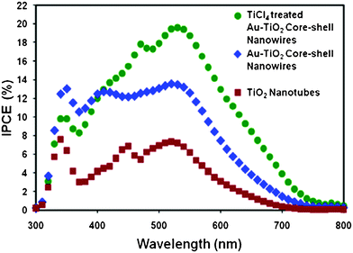 | ||
| Fig. 8 IPCE spectra of DSSCs based on TiO2 nanotubes, Au–TiO2 core-shell nanowires, and TiCl4 treated Au–TiO2 core-shell nanowires. | ||
To evaluate the influence of gold insertion and TiCl4 treatment on the dye adsorption on the photoanodes, the amount of chemisorbed dye was evaluated by desorption followed by quantitation with UV-Vis absorbance spectroscopy (Table 2). The amount of dye on each of the nanotube and nanowire structures was not substantially different even with TiCl4 treatment. However, the mesoporous TiO2 nanoparticle film alone demonstrated at least a 15% higher dye loading even though it was only half as thick as the anodes with both the mesoporous film and a nanotube or nanowire array combined. This result suggests that the adhesion layer was not effectively coated with dye when it was underneath a nanotube or nanowire array. Since overall dye loading was similar for all devices, other factors must have contributed to enhanced photocurrent for the Au–TiO2 and TiCl4 treated arrays. Most likely causes include increased light absorbance due to scattering and increased electron transport due to conducting pathways added by the gold nanowires. The former is related to light scattering due to the metallic gold in the Au–TiO2 nanowires or TiO2 particles deposited by TiCl4 treatment. This explanation is consistent with other findings.54–55 While IPCE data suggest enhancements due to scattering, additional studies are needed to fully assess the role of both light enhancement effects and electron transport effects. Ongoing investigations aim to elucidate details of the mechanisms that resulted in higher efficiencies for the core-shell devices.
Conclusions
We synthesized novel Au–TiO2 core-shell nanoarchitectures and used them in dye sensitized solar cells. Adding gold cores to TiO2 nanotubes resulted in a two-fold improvement in efficiency compared to hollow TiO2 nanotubes. This improvement is likely the result of a combination of 1) improved pathways for electron transport out of the anode after photoinduced charge injection and 2) light focusing effects caused by the metal nanostructures. Furthermore, removing the partially insulating nanocrystalline TiO2 nanoparticle layer form the bottom of the nanostructures resulted in significant improvements, suggesting that direct contact of the nanowire arrays with the conducting substrate is an important condition for good efficiency. For core-shell structures with an oxide thickness of less than 20 nm and a core conductor that spans the entire length of the tubes, electrons injected into the oxide only have to travel around 20 nm before reaching a conductor. As a consequence, the use of fast redox couples like ferrocene may become possible with dye cells based on these core-shell structures. Further treatment of the core-shell structures with TiCl4 resulted in an additional improvement in the efficiency. This improvement is likely caused by additional light scattering effects. The dye cells with core-shell photoanodes increased the current generation substantially, thereby increasing the solar conversion efficiencies. Au–TiO2 core-shell structures treated with TiCl4 exhibited a four fold enhancement in cell efficiency compared to untreated TiO2 nanotubes, suggesting that the new structures may lead to improved methods for producing more efficient DSSCs. Continuing studies aim to develop further improvements by increasing the length and surface area of TiO2 as well as utilizing alternate redox couples. Although this proof of concept study utilized gold as the core, use of less expensive metals as the core material will decrease the cost for these core-shell nanowire photovoltaic architectures.Acknowledgements
This work was supported by the Louisiana Board of Regents, LEQSF (2007-12)-ENH-PKSFI-PRS-04 and LEQSF (2008-13)-GF-19. The authors acknowledge assistance from Prof. J. B. Wiley and Jin Hee Lim for providing the potentiostat and electrodeposition training.References
- B. Oregan, J. Moser, M. Anderson and M. Gratzel, J. Phys. Chem., 1990, 94, 8720 CrossRef CAS.
- B. Oregan and M. Gratzel, Nature, 1991, 353, 737 CrossRef CAS.
- N. Kopidakis, E. A. Schiff, N. G. Park, J. van de Lagemaat and A. J. Frank, J. Phys. Chem. B, 2000, 104, 3930 CrossRef CAS.
- M. Law, L. E. Greene, J. C. Johnson, R. Saykally and P. D. Yang, Nat. Mater., 2005, 4, 455 CrossRef CAS.
- K. Keis, E. Magnusson, H. Lindstrom, S. E. Lindquist and A. Hagfeldt, Sol. Energy Mater. Sol. Cells, 2002, 73, 51 CrossRef.
- K. Fujihara, A. Kumar, R. Jose, S. Ramakrishna and S. Uchida, Nanotechnology, 2007, 18 Search PubMed.
- T. Beppu, S. Yamaguchi and S. Hayase, Japanese Journal of Applied Physics Part 1-Regular Papers Brief Communications & Review Papers, 2007, 46, 4307 CAS.
- E. Enache-Pommer, J. E. Boercker and E. S. Aydil, Applied Physics Letters, 2007, 91 Search PubMed.
- J. E. Boercker, E. Enache-Pommer and E. S. Aydil, Nanotechnology, 2008, 19 Search PubMed.
- X. J. Feng, K. Shankar, O. K. Varghese, M. Paulose, T. J. Latempa and C. A. Grimes, Nano Lett., 2008, 8, 3781 CrossRef CAS.
- W. L. Wang, H. Lin, J. B. Li and N. Wang, J. Am. Ceram. Soc., 2008, 91, 628 CrossRef CAS.
- R. Jose, V. Thavasi and S. Ramakrishna, J. Am. Ceram. Soc., 2009, 92, 289 CrossRef CAS.
- M. Paulose, K. Shankar, O. K. Varghese, G. K. Mor, B. Hardin and C. A. Grimes, Nanotechnology, 2006, 17, 1446 CrossRef CAS.
- T. S. Kang, A. P. Smith, B. E. Taylor and M. F. Durstock, Nano Lett., 2009, 9, 601 CrossRef CAS.
- G. K. Mor, K. Shankar, M. Paulose, O. K. Varghese and C. A. Grimes, Nano Lett., 2006, 6, 215 CrossRef CAS.
- J. M. Macak, H. Tsuchiya, A. Ghicov, K. Yasuda, R. Hahn, S. Bauer and P. Schmuki, Curr. Opin. Solid State Mater. Sci., 2007, 11, 3 CrossRef CAS.
- S. Berger, H. Tsuchiya and P. Schmuki, Chem. Mater., 2008, 20, 3245 CrossRef CAS.
- S. M. Liu, L. M. Gan, L. H. Liu, W. D. Zhang and H. C. Zeng, Chem. Mater., 2002, 14, 1391 CrossRef CAS.
- P. V. Kamat, J. Phys. Chem. C, 2007, 111, 2834 CAS.
- M. L. Wang, C. G. Huang, Y. G. Cao, Q. J. Yu, Z. H. Deng, Y. Liu, Z. Huang, J. Q. Huang, Q. F. Huang, W. Guo and J. K. Liang, J. Phys. D: Appl. Phys., 2009, 42, 155104 CrossRef.
- M. Law, L. E. Greene, A. Radenovic, T. Kuykendall, J. Liphardt and P. D. Yang, J. Phys. Chem. B, 2006, 110, 22652 CrossRef CAS.
- S. Chappel, S. G. Chen and A. Zaban, Langmuir, 2002, 18, 3336 CrossRef CAS.
- H. Arakawa, Nippon Kagakkai Koen Yokoshu, 2001, 86, 16 Search PubMed.
- A. B. F. Martinson, J. W. Elam, J. Liu, M. J. Pellin, T. J. Marks and J. T. Hupp, Nano Lett., 2008, 8, 2862 CrossRef CAS.
- Y. Xie, L. Zhou, C. Huang, H. Huang and J. Lu, Electrochim. Acta, 2008, 53, 3643 CrossRef CAS.
- S. Banerjee, S. K. Mohapatra, P. P. Das and M. Misra, Chem. Mater., 2008, 20, 6784 CrossRef CAS.
- Q. Wang, K. Zhu, N. R. Neale and A. J. Frank, Nano Lett., 2009, 9, 806 CrossRef CAS.
- S. K. Mohapatra, N. Kondamudi, S. Banerjee and M. Misra, Langmuir, 2008, 24, 11276 CrossRef CAS.
- S. G. Chen, M. Paulose, C. Ruan, G. K. Mor, O. K. Varghese, D. Kouzoudis and C. A. Grimes, J. Photochem. Photobiol., A, 2006, 177, 177 CrossRef CAS.
- D. Fang, K. L. Huang, S. Q. Liu and D. Y. Qin, Electrochem. Commun., 2009, 11, 901 CrossRef CAS.
- H. Y. Zhang, T. H. Ji, Y. F. Liu and J. W. Cai, J. Phys. Chem. C, 2008, 112, 8604 CAS.
- M. Gratzel, Philos. Trans. R. Soc. London, Ser. A, 2007, 365, 993 CrossRef CAS.
- N. S. Lewis and D. G. Nocera, Proc. Natl. Acad. Sci. U. S. A., 2006, 103, 15729 CrossRef CAS.
- W. Zhu, G. Z. Wang, X. Hong, X. S. Shen, D. P. Li and X. Xie, Electrochim. Acta, 2009, 55, 480 CrossRef CAS.
- W. Zhu, G. Z. Wang, X. Hong and X. S. Shen, J. Phys. Chem. C, 2009, 113, 5450 CAS.
- H. Q. An, J. X. Li, J. Zhou, K. R. Li, B. L. Zhu and W. P. Huang, J. Mater. Chem., 2010, 20, 603 RSC.
- S. K. Mohapatra, S Banerjee and M. .Misra, Nanotechnology, 2008, 19 Search PubMed.
- C. J. Barbe, F. Arendse, P. Comte, M. Jirousek, F. Lenzmann, V. Shklover and M. Gratzel, J. Am. Ceram. Soc., 1997, 80, 3157 CrossRef CAS.
- N. G. Park, G. Schlichthorl, J. van de Lagemaat, H. M. Cheong, A. Mascarenhas and A. J. Frank, J. Phys. Chem. B, 1999, 103, 3308 CrossRef CAS.
- M. K. Nazeeruddin, A. Kay, I. Rodicio, R. Humphrybaker, E. Muller, P. Liska, N. Vlachopoulos and M. Gratzel, J. Am. Chem. Soc., 1993, 115, 6382 CrossRef CAS.
- L. Y. Zeng, S. Y. Dai, K. J. Wang, X. Pan, C. W. Shi and L. Guo, Chin. Phys. Lett., 2004, 21, 1835 CrossRef CAS.
- P. Charoensirithavorn, Y. Ogomi, T. Sagawa, S. Hayase and S. Yoshikawaa, J. Electrochem. Soc., 2010, 157, B354 CrossRef CAS.
- D. Menzies, Y. B. Cheng, G. P. Simon and L. Spiccia, Journal of the Australasian Ceramic Society, 2003, 39, 108 CAS.
- B. C. O'Regan, J. R. Durrant, P. M. Sommeling and N. J. Bakker, J. Phys. Chem. C, 2007, 111, 14001 CAS.
- C. T. Yip, C. S. K. Mak, A. B. Djurisic, Y. F. Hsu and W. K. Chan, Appl. Phys. A: Mater. Sci. Process., 2008, 92, 589 CrossRef CAS.
- E. A. Barringer and H. K. Bowen, Langmuir, 1985, 1, 414 CrossRef CAS.
- A. Siegel, M. R. Goncalves, R. Ameling and O. Marti, J. Opt. A: Pure Appl. Opt., 2007, 9, S443 CrossRef.
- P. M. Sommeling, B. C. O'Regan, R. R. Haswell, H. J. P. Smit, N. J. Bakker, J. J. T. Smits, J. M. Kroon and J. A. M. van Roosmalen, J. Phys. Chem. B, 2006, 110, 19191 CrossRef CAS.
- S. Ito, T. N. Murakami, P. Comte, P. Liska, C. Gratzel, M. K. Nazeeruddin and M. Gratzel, Thin Solid Films, 2008, 516, 4613 CrossRef CAS.
- C. J. Lin, W. Y. Yu and S. H. Chien, J. Mater. Chem., 2010, 20, 1073 RSC.
- Q. W. Chen and D. S. Xu, J. Phys. Chem. C, 2009, 113, 6310 CAS.
- V. E. Ferry, J. N. Munday and H. A. Atwater, Adv. Mater., 2010, 22, 4794 CrossRef CAS.
- H. A. Atwater and A. Polman, Nat. Mater., 2010, 9, 205 CrossRef CAS.
- Z. S. Wang, H. Kawauchi, T. Kashima and H. Arakawa, Coord. Chem. Rev., 2004, 248, 1381 CrossRef CAS.
- L. H. Hu, S. Y. Dai, J. Weng, S. F. Xiao, Y. F. Sui, Y. Huang, S. H. Chen, F. T. Kong, X. Pan, L. Y. Liang and K. J. Wang, J. Phys. Chem. B, 2007, 111, 358 CrossRef CAS.
Footnote |
| † Electronic Supplementary Information (ESI) available. See DOI: 10.1039/c1ra00762a/ |
| This journal is © The Royal Society of Chemistry 2012 |