Micro free-flow electrophoresis with injection molded chips†
Stefan
Köhler
a,
Christian
Benz
a,
Holger
Becker
b,
Erik
Beckert
c,
Volker
Beushausen
d and
Detlev
Belder
*a
aInstitute of Analytical Chemistry, University of Leipzig, Linnéstr, 3, 04103, Leipzig, Germany. E-mail: belder@uni-leipzig.de
bMicrofluidic ChipShop GmbH, Carl-Zeiss-Promenade 10, 07745, Jena, Germany
cFraunhofer-Institut für Angewandte Optik und Feinmechanik, Albert-Einstein-Str. 7, 07745, Jena, Germany
dLaser-Laboratorium Göttingen e.V., Hans-Adolf-Krebs-Weg 1, 37077, Göttingen, Germany
First published on 16th November 2011
Abstract
In this work we present an approach towards economic free-flow electrophoresis chips fabricated by injection molding as mass replication process. This is achieved by the development of a free-flow electrophoresis chip design suitable for one step molding fabrication. Integrated partitioning bars are incorporated as key elements for bubble segregation. A defined open gap of 20 μm in height and 500 μm in width was integrated between the separation chamber and the electrode channels, acting as a barrier for gas bubbles while maintaining electrical contact by the fluidic junction. Additionally, we present an approach to avoid internal electrodes in FFE microchips for a facile mass production process. The injection molded thermoplastic μFFE chips are ready to use without subsequent labor-intensive implementation of membranes or comparable structures serving as salt bridges.
Introduction
Micro free-flow electrophoresis (μFFE) is a miniaturized analytical method, which allows continuous high-speed electroseparations for a wide field of applications ranging from small molecules like fluorescent dyes up to large compounds like cell organelles.1,2 Its beneficial properties compared to macroscopic FFE include higher speed, portability and tremendously decreased sample and reagent consumption.3,4 Especially with an online-coupled detection method μFFE could function as one key element for micropreparative separations and analysis in complex lab-on-a-chip devices, e.g. in succession of sample preparation and multistep chemical reactions.5–9The development of μFFE is a lively field starting with the first device made of silicon presented in 1994 by Raymond et al.10 The design, which features two side channel arrays working as a junction between electrode segments and a separation chamber, was numerously applied in continuative studies.11–15 One of the main challenges in μFFE is the effective electrical connection between the electrodes and the separation region ensuring both a good electrical connection and an efficient barrier for electrolysis products like gas bubbles.
In conventional large-scale FFE devices this problem is usually circumvented by manual integration of ion permeable membranes between electrode channels and separation chamber.16 A comparable approach suitable for μFFE was presented by Kohlheyer et al. and Albrecht et al. showing microchips with polymerized ion permeable acryl amide membranes.17–20 This approach revealed excellent retention of gas bubbles but limited chemical and mechanical stability of the membranes.
An alternative to the laborious implementation of membranes or membrane like structures is the use of open fluidic connections. This approach strongly reduces voltage drops resulting in high electrical field strengths. Since electrolysis products can interfere with the separation in this design, Fonslow et al. and Kostal et al. implemented deeper electrode beds to gain higher flow rates for improved bubble removal.21–23 A challenge of these methods is the need for a very precise flow adjustment.
Further approaches for effective voltage application to the electrophoretic process bed combined with proper bubble retention include narrow side banks,24 electrostatic induction,25 rupture salt bridge junction points26 and electrochemical water electrolysis suppression.27
Recently we reported on a new μFFE chip design with integrated monolithic partitioning bars for bubble segregation which offers both high voltage efficiency and effective gas bubble retention.28 The presented PDMS chips were fabricated by rapid and facile softlithographic casting.
Nevertheless, almost all presented microfluidic free-flow electrophoresis devices to date suffer from their lack of mass fabrication capabilities. The chips utilize several strategies for bubble segregation, fluidic handling and, regarding the case of free-flow isoelectric focusing, pH gradient formation. For this, the presenting workgroups use either materials requiring laborious and expensive fabrication steps or equally laborious integration procedures for membranes and electrodes.
Herein we present a new approach towards thermoplastic μFFE chips that are capable for fast and cheap mass fabrication. The design features an optimized partitioning bar layout in order to enable an economic one-step injection molding process. Additionally, we evaluate an alternative electrode approach for avoiding the cost and labor-intensive implementation of integrated metal electrodes. The devices were successfully applied for free-flow zone electrophoretic separations in various applications including the separation of amines, amino acids and proteins.
Experimental
Chip design
The 25 mm × 75 mm polymer chips consist of five separation chamber inlets for running buffer and sample solutions and one inlet and outlet each for the two adjacent electrode channels. In order to obtain a consistent flow profile in the separation chamber, the drain outlets are designed in the shape of a channel array consisting of 25 narrow channels of equal width connected upstream to five outlet channels. The 50 μm high separation chamber is 14 mm wide and 28 mm long. To prevent the large chamber from collapsing, pillars with a diameter of 500 μm are introduced at intervals of 2 mm along the chamber length and width. The 500 μm × 300 μm (width × height) electrode channels are separated from the separation area by two monolithic partitioning bars which reduce the in-between channel height to 20 μm along the whole length of the separation chamber in a space of 500 μm (Fig. 1). Compared to our previous design28 the electrode channel height is increased for an improved bubble removal.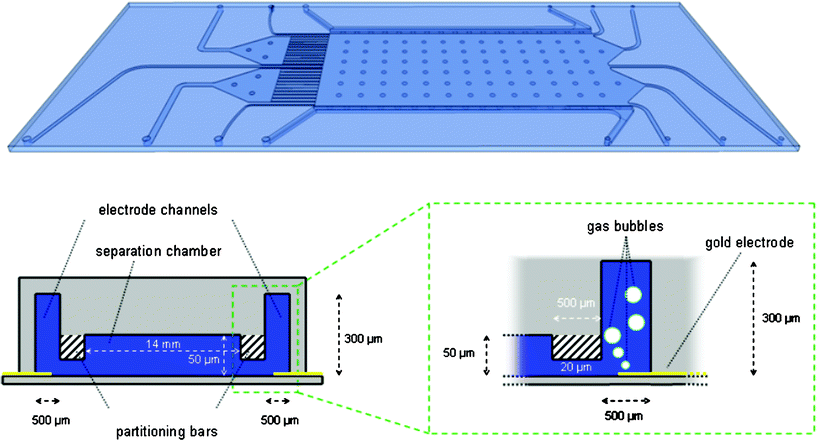 | ||
| Fig. 1 Chip layout and cross-sectional diagram of the separation chamber, the electrode channels and the partitioning bars showing the principle of bubble retention. | ||
The chips can be operated each with integrated or external electrodes. The integrated electrodes are fabricated by deposition of a thin conductive structure on the sealing polymer layer by metal sputtering or printing with metal slurry ink. For operation with external electrodes, thin metal wires are introduced into the inlet and outlet tubes of the electrode channels (Fig. 2). In order to expand the applicability of the chips we developed a second design which features a circular chamber in the center outlet channel. It is envisaged as an access port for the prospective integration of auxiliary detection approaches, e.g. the integration of SERS targets, ELISA binding sites or chemical sensors.
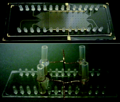 | ||
| Fig. 2 COP chip with integrated gold electrodes (upper picture) and COP chip with external copper wire electrodes (lower picture). | ||
Materials and reagents
Rhodamine 6G, sulforhodamine B, rhodamine B, 7-amino-4-methylcoumarin (coumarin 120), fluorescein-5-isothiocyanate (FITC, isomer I), β-lactoglobulin, carboanhydrase I, trypsinogen, 2-butylamine, glycine, aspartic acid, (hydroxypropyl)-methylcellulose (HPMC), 2-(cyclohexylamino)ethane-sulfonic acid (CHES), 4-(2-hydroxyethyl)piperazine-1-ethanesulfonic acid (HEPES) and Tween 20 were purchased from Sigma-Aldrich-Fluka, sodium tetraborate, sodium acetate, ammonium acetate, sodium hydroxide, hydrochloric acid and methanol from Merck. Fluorescein (sodium salt) was purchased from Roth, Alexa Fluor 488 5-tetrafluorophenyl ester (AF488 5-TFP) was from Invitrogen. B-phycoerythrin solution (11 mg ml−1) was purchased from AnaSpec, green fluorescent protein solution (StrII-eGFP, 1.1 mg ml−1) from IBA. Stock solutions of fluorescein (5 mg ml−1), rhodamine B (3 mg ml−1), rhodamine 6G (3 mg ml−1) and sulforhodamine B (3 mg ml−1) were prepared in demineralized water. Coumarin 120 stock solution (5 mg ml−1) was prepared in methanol. 2-Butylamine, glycine and aspartic acid were labeled with FITC as described previously.29 Labeling of trypsinogen, carboanhydrase I and β-lactoglobulin with AF488 5-TFP was carried out using the label protocol provided by Invitrogen. Sample solutions were prepared right before experiments by diluting from the stocks. To avoid air bubbles, the running buffer solutions were degassed in vacuum.Chip fabrication
The body of the chips was manufactured by injection molding on a 80 ton clamping force injection molding machine using a mold-base for microscopy slide-sized exchangeable mold inserts. For our studies we used cycloolefin polymer (COP), tradename Zeonor, as chip material.The sputtered integrated electrodes were formed using an electron-beam evaporation process of 10 nm titanium as adhesion promoter and 100 nm gold on a 188 μm thick Zeonor foil. A laser-cut stainless steel sheet was used as a shadow mask to generate the electrode pattern. Subsequently, chip body and cover foil were bonded.
External electrodes were realized using flexible silicone tubes for fluidics and thin copper wires. The wires were simply inserted in the tubes and sealed with silicone adhesive.
Due to the hydrophobic nature of COP, bubble free filling of the chips with aqueous solutions is challenging. This difficulty could be overcome by channel surface hydrophilization using a low pressure air plasma treatment prior to usage. Although there is a general potential of chip damage due to heating at conductive metal parts, the plasma treatment was also possible with chips featuring integrated electrodes without any evoked malfunction of the hydrophilized chips.
Experimental setup
The chips were connected to syringe pumps using PTFE capillary tubes (Supelco, USA). For sample solutions (center inlet) and the two adjacent buffer inlets, a pulsation free multi-channel syringe pump (neMESYS, cetoni, Germany) equipped with high precision glass syringes (ILS, Germany) was utilized. The electrode channels were connected to a two-channel syringe pump (PHD 2000, Harvard Apparatus, USA) with plastic syringes. For FFZE operation, the two outer separation bed inlets were not used and sealed before experiments. Electrical contact to the high voltage power supply (HCL 35–6500, FuG Elektronik, Germany) was achieved by integrated as well as external electrodes.Fluorescent dye separations were carried out using a 366 nm UV-lamp as excitation source without further filters. Separations of biomolecules were performed on a fluorescence microscope (IX71, Olympus) with mercury burner and fluorescence filter sets for FITC (U-MWB2, Olympus) and FITC/Cy3/Cy5 (LOT-Oriel, Germany). For monitoring and data acquisition a digital camera (NV-GS400 or DMC-FS7, Panasonic) was mounted on the microscope or above the respective chip assembly.
The sample solutions were injected through the center separation bed inlet and were flanked by running buffer streams introduced through the adjacent separation bed inlets. The electrode channels were equally flushed with buffer solution.
FFE electropherograms were extracted from images by line scan evaluation using ImageJ. For a better visualization, contrast and brightness of the displayed separation images were subsequently adjusted.
For the comparison of our electrode approaches we used a two component fluorescent dye sample mixture consisting of fluorescein and rhodamine B (500 μg ml−1 each) in aqueous methanol (50 vol.%). 20 mM HEPES buffer solution at a pH of 7.5 with 0.1% Tween 20 and 0.2% HPMC was utilized as running buffer. Since rhodamine B is uncharged at this pH value, it was used as reference for the migration distance of the fluorescein band.
The electrophoretic mobility of fluorescein at experimental conditions was determined by capillary zone electrophoresis using 20 mM HEPES buffer at pH 7.5 without HPMC and Tween 20 addition. Rhodamine B was added as EOF marker.
In order to gain a stable flow profile running buffer streams in the separation bed were partially dissipated through the electrode channels by adjusting the hydrostatic backpressure between separation bed outlets and electrode channel outlets. Thus, the residence time of analytes calculated from the linear velocity, dependent on flow rates, is slightly increased.
Results and discussion
The chip layout presented in Fig. 1 and 2 was designed for facile integration of all necessary components in one mold-base, enabling a one-step molding fabrication process for the functional fluidic structure. For this, we integrated partitioning bars between the separation chamber and electrode channels in order to hinder gas bubbles from entering the separation area while maintaining fluidic and electric connections. Due to the open gap architecture a rather high voltage efficiency is achieved as tested and evaluated previously with PDMS prototype chips.28For the injection molded COP chips we modified the previous design to enhance the gas bubble removal capacity. We increased the height of the electrode channels from 50 μm to 300 μm resulting in extended volume for capturing gas bubbles while they are continuously flushed out by the electrode buffer streams. Additionally, gas bubble interactions within the separation chamber are furthermore reduced since ascending gas bubbles are captured at the electrode channel top side away from the fluidic junction. This turned out to be useful especially when working with very high electrical currents and only moderate flow velocities in the electrolyte channels.
Compared to the previous layout of the PDMS prototype chips the separation chamber dimensions were increased to achieve a higher flexibility for different applications. With the 2.5 times longer separation chamber the residence time of samples in the electrical field is increased, resulting in enhanced separation performance. If a longer residence time is not necessary, the enlarged chamber length permits higher flow velocities which helps in reducing band broadening effects caused by diffusion.30,31 The five times wider chamber increases the number of analytes to be separated during one experiment. Additionally, the expanded width provides free space for hydrodynamic band steering. However, the outer dimensions still match the size of standard microscopy glass slides.
Since the aspect of several design elements including separation chamber and partitioning bars were enlarged, it was found to be necessary to introduce small pillars to prevent the chamber from collapsing during the bonding process. Although the pillars seem to act as obstacles, they did not impede the electrophoretic performance.
In order to enable quick and facile implementation of the fluidics, the chips include integrated ports for direct fluidic tube connection, which allowed very convenient handling in daily use.
While the one-step manufacturing process appeared to be ideally suited for mass fabrication of the fluidic chamber, the laborsome implementation of sputtered electrodes was found to spoil the applicability for mass production of fully functional devices. To meet this challenge we investigated approaches using external electrodes instead of the internal type.
In our experiments we employed two types of electrodes. The classic chip integrated electrodes consist of a thin gold layer on the sealing polymer foil in the area of the electrode channels with outer contacts for the connection to the power supply. In contrast, external electrodes were realized by simple incorporation of thin metal wires into the inlet and outlet fluid tubes connected to the electrode channels. In Fig. 3 the employed chips with integrated electrodes as well as electrode-less versions for the usage with external electrodes are illustrated.
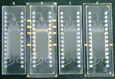 | ||
| Fig. 3 Utilized COP chips. a) electrode-less design with detection target chamber, b) design with detection target chamber and integrated electrodes, c) electrode-less standard design, d) standard design with integrated gold electrodes. | ||
An intensive comparison of both approaches revealed a better voltage efficiency with the integrated electrodes as expected. The voltage efficiency of 90% is superior to the measured 30% achieved with external electrodes.
Surprisingly though the external electrode approach was well applicable as all experiments could be carried out with both electrode types without significant differences in the obtained results. The applied voltages, however, had to be increased using external electrodes in order to achieve comparable field strengths. Due to the ease of application we meanwhile use this approach almost exclusively in our laboratory. A further feature of the external electrode setup is that the gas bubbles are primarily generated within the fluidic connections. The usage of gas permeable tubes would allow to elegantly remove the bubbles analogous to an online degasser in HPLC. Corresponding investigations are under way in our laboratory.
The application of the COP chips could be successfully demonstrated by free-flow zone electrophoretic separations of multiple fluorescent dyes. Fig. 4 illustrates the separation of fluorescein, sulforhodamine B, coumarin 120 and rhodamine 6G. At the experimental conditions using HEPES buffer at a pH of 7.5, fluorescein is doubly charged and sulforhodamine B carries one negative charge leading to migrations of both analytes to the anode. Coumarin 120 is uncharged and therefore not affected electrophoretically by the electric field while rhodamine 6G is positively charged and migrates to the cathode.
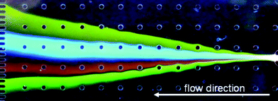 | ||
| Fig. 4 Free-flow zone electrophorectic separation of four fluorescent dyes. Analytes top down: rhodamine 6G, coumarin 120, sulforhodamine B, fluorescein. Separation in 10 mM HEPES buffer pH 7.5, 0.1% HPMC, 0.1% Tween 20 at 589 V using external electrodes. | ||
As the device performed well with simple dye test mixtures we extended our studies to some more demanding applications such as the separation of amines, amino acids and proteins. In order to enable fluorescence detection, non fluorescent analytes were labeled prior to analysis.
Fig. 5 shows the separation of FITC-labeled 2-aminobutane, glycine and aspartic acid. A fourth signal is caused by hydrolyzed FITC which forms a discrete band beside the analytes. Therefore, it can easily be removed from sample mixtures directly during separation experiments making preliminary purification steps unnecessary.
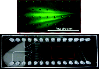 | ||
| Fig. 5 FFZE of FITC-labeled 2-aminobutane, glycine and aspartic acid including a separated band of hydrolyzed FITC. Separation in 20 mM CHES buffer pH 8, 0.1% HPMC, 0.1% Tween 20 at 566 V using external electrodes. | ||
The detection of separated proteins at low concentration turned out to be more challenging. In order to record the separations we had to use a higher magnifying objective. Thus, the observable chip area was relatively small-sized compared to the whole separation chamber dimension.
Nevertheless we were able to visualize the μFFE separation of AF488 labeled β-lactoglobulin, carboanhydrase I and trypsinogen as shown in Fig. 6. The separation was recorded at the separation chamber inlet showing the sample stream splitting into three bands immediately after entering the separation chamber. Although the separated bands could not be traced at the outlet with the used detection assembly, the outlet point of the single bands can be determined by their constant deflection angles in free-flow zone electrophoresis mode (course indicated by inserted dashed blue lines).
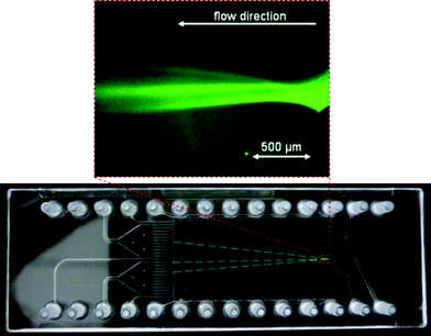 | ||
| Fig. 6 Separation of Alexa Fluor 488 labeled β-lactoglobulin, carboanhydrase I and trypsinogen in 10 mM acetate buffer pH 5, 0.2% HPMC, 0.1% Tween 20 at 331 V using external electrodes. | ||
One envisaged application of the chips is the on-chip sample purification of small sample amounts and online monitoring purposes of native biomolecules. Therefore, the separation performance for native proteins was investigated. Since intrinsic fluorescence in the deep UV range is not possible with polymer chips, we used the native green fluorescent protein StrII-eGFP and the native red fluorescent protein B-phycoerythrin for our studies. As shown in Fig. 7 we were able to separate both proteins into two distinct bands which proves that our COP chips are also applicable to native biomolecules.
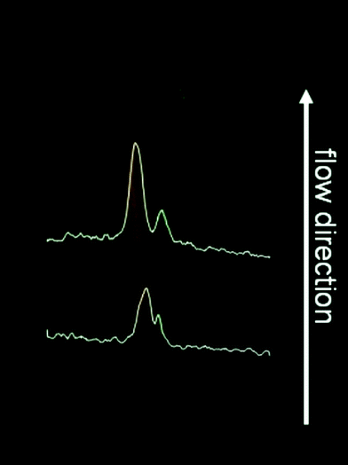 | ||
| Fig. 7 FFZE of the native proteins B-phycoerythrin (red fluorescent, left) and StrII-eGFP (green fluorescent, right) using 10 mM ammonium acetate buffer pH 5, 0.1% HPMC, 0.1% Tween 20. Separation voltage 577 V, external electrodes. | ||
In order to prevent adsorption of the proteins to the chip walls a careful surface deactivation was found to be essential for protein separations. We investigated several approaches for surface coating, such as permanent coatings with polyvinylalcohol32 or with immobilised polyethyleneglycol. However, for ease of handling a dynamic surface modification with HPMC added to the buffer turned out to be the method of choice.
During our studies we tested around 30 COP chips from several batches without significant performance differences from chip to chip, demonstrating the robustness of the mass manufacturing process.
Conclusions
In this work, a polymer microfluidic free-flow electrophoresis device with optional integrated or external electrodes is presented. The chips were produced by injection molding as mass replication process and were successfully used for separating sample mixtures of a wide variety, including fluorescent dyes, small amines and amino acids as well as labeled and native proteins. It was found that the chips can be used without laboriously generated sputtered electrodes which facilitates an economic mass production. The chip design includes monolithic partitioning bars reducing the in-between channel height of the electrode channels and the separation chamber. This way, gas bubbles formed by water electrolysis are hindered from entering the separation chamber while being continuously flushed out by the electrode buffer flow.Acknowledgements
Funding for this research was provided by the German Federal Ministry of Education and Research, grant no. 01RI0643B and by the DFG (Deutsche Forschungsgemeinschaft).References
- H. Lu, S. Gaudet, M. A. Schmidt and K. F. Jensen, Anal. Chem., 2004, 76, 5705–5712 CrossRef CAS.
- V. Kostal, B. R. Fonslow, E. A. Arriaga and M. T. Bowser, Anal. Chem., 2009, 81, 9267–9273 CrossRef CAS.
- D. Kohlheyer, J. C. T. Eijkel, A. van den Berg and R. B. M. Schasfoort, Electrophoresis, 2008, 29, 977–993 CrossRef CAS.
- N. Pamme, Lab Chip, 2007, 7, 1644–1659 RSC.
- D. Belder, Angew. Chem., Int. Ed., 2009, 48, 3736–3737 CrossRef CAS.
- G. M. Whitesides, Nature, 2006, 442, 368–373 CrossRef CAS.
- A. J. deMello, Nature, 2006, 442, 394–402 CrossRef CAS.
- D. Mark, S. Haeberle, G. Roth, F. von Stetten and R. Zengerle, Chem. Soc. Rev., 2010, 39, 1153–1182 RSC.
- A. van den Berg and T. S. J. Lammerink, Top. Curr. Chem., 1998, 194, 21–49 CrossRef CAS.
- D. E. Raymond, A. Manz and H. M. Widmer, Anal. Chem., 1994, 66, 2858–2865 CrossRef CAS.
- D. E. Raymond, A. Manz and H. M. Widmer, Anal. Chem., 1996, 68, 2515–2522 CrossRef CAS.
- C.-X. Zhang and A. Manz, Anal. Chem., 2003, 75, 5759–5766 CrossRef CAS.
- B. R. Fonslow and M. T. Bowser, Anal. Chem., 2005, 77, 5706–5710 CrossRef CAS.
- D. Janasek, M. Schilling, J. Franzke and A. Manz, Anal. Chem., 2006, 78, 3815–3819 CrossRef CAS.
- Y. S. Huh, T. J. Park, K. Yang, E. Z. Lee, Y. K. Hong, S. Y. Lee, D. H. Kim and W. H. Hong, Ultramicroscopy, 2008, 108, 1365–1370 CrossRef CAS.
- A. Chartogne, U. R. Tjaden and J. van der Greef, Rapid Commun. Mass Spectrom., 2000, 14, 1269–1274 CrossRef CAS.
- D. Kohlheyer, G. A. J. Besselink, S. Schlautmann and R. B. M. Schasfoort, Lab Chip, 2006, 6, 374–380 RSC.
- D. Kohlheyer, J. C. T. Eijkel, S. Schlautmann, A. van den Berg and R. B. M. Schasfoort, Anal. Chem., 2007, 79, 8190–8198 CrossRef CAS.
- J. W. Albrecht and K. F. Jensen, Electrophoresis, 2006, 27, 4960–4969 CrossRef CAS.
- J. W. Albrecht, J. El-Ali and K. F. Jensen, Anal. Chem., 2007, 79, 9364–9371 CrossRef CAS.
- B. R. Fonslow, V. H. Barocas and M. T. Bowser, Anal. Chem., 2006, 78, 5369–5374 CrossRef CAS.
- B. R. Fonslow and M. T. Bowser, Anal. Chem., 2008, 80, 3182–3189 CrossRef CAS.
- V. Kostal, B. R. Fonslow, E. A. Arriaga and M. T. Bowser, Anal. Chem., 2009, 81, 9267–9273 CrossRef CAS.
- H. Kobayashi, K. Shimamura, T. Akaida, K. Sakano, N. Tajima, J. Funazaki, H. Suzuki and E. Shinohara, J. Chromatogr., A, 2003, 990, 169–178 CrossRef CAS.
- D. Janasek, M. Schilling, A. Manz and J. Franzke, Lab Chip, 2006, 6, 710–713 RSC.
- Y.-A. Song, M. Chan, C. Celio, S. R. Tannenbaum, J. S. Wishnok and J. Han, Anal. Chem., 2010, 82, 2317–2325 CrossRef CAS.
- D. Kohlheyer, J. C. T. Eijkel, S. Schlautmann, A. van den Berg and R. B. M. Schasfoort, Anal. Chem., 2008, 80, 4111–4118 CrossRef CAS.
- S. Köhler, C. Weilbeer, S. Howitz, H. Becker, V. Beushausen and D. Belder, Lab Chip, 2011, 11, 309–314 RSC.
- D. Belder, A. Deege, M. Maass and M. Ludwig, Electrophoresis, 2002, 23, 2355–2361 CrossRef CAS.
- M. Poggel, T. Melin and S. Treutlein, Electrophoresis, 2002, 23, 2252–2258 CrossRef CAS.
- B. R. Fonslow and M. T. Bowser, Anal. Chem., 2006, 78, 8236–8244 CrossRef CAS.
- D. Belder, A. Deege, F. Kohler and M. Ludwig, Electrophoresis, 2002, 23, 3567–3573 CrossRef CAS.
Footnote |
| † Our work is dedicated to the memory of Volker Beushausen who passed away during the course of this project. |
| This journal is © The Royal Society of Chemistry 2012 |
