Light-controlled self-assembly and conductance: from nanoribbons to nanospheres†
Lulu
Ma
a,
Jiong
Jia
c,
Tieying
Yang
d,
Guangzhi
Yin
d,
Yang
Liu
a,
Xuan
Sun
*b and
Xutang
Tao
*a
aState Key Laboratory of Crystal Materials, Shandong University, Jinan 250100, P. R. China. E-mail: txt@icm.sdu.edu.cn; Tel: +86-531-88364963
bKey laboratory of Colloid and Interface Chemistry, Ministry of Education, School of Chemistry and Chemical Engineering, Shandong University, Jinan 250100, P. R. China. E-mail: sunxuan@sdu.edu.cn; Tel: +86-531-88362326
cSchool of Chemistry and Chemical Engineering, Shandong University, Jinan 250100, P. R. China
dShanghai Institute of Applied Physic, Chinese Academy of Science, Shanghai 201204, P. R. China
First published on 10th February 2012
Abstract
Photoswitchable azobenzene (AZO) chromophores were introduced to the bay-position of the traditional n-type perylene diimide (PDI). Photocontrolled self-assembly behaviours and the influence of the azobenzene substitution on the assembly structure were investigated by UV/vis spectroscopy, scanning electron microscopy (SEM), transmission electron microscopy (TEM), X-ray diffraction (XRD) and atomic force microscopy (AFM). Controlled morphological evolution of the nanostructures from ribbons to spheres was facilely realized by driving the azobenzene switching unit with 365 nm light irradiation. The nanoribbons demonstrated highly ordered structures while the order of the molecular arrangement was destroyed in the nanospheres, as a result of the curved molecular conformation induced by photoisomerization. In addition, the conductivity of the single nanoribbon was investigated. Thanks to the one-dimensional long-range ordered π–π stacking of the PDI cores, the nanoribbon showed good semiconducting properties with a conductance in the range of 2 × 10⁻⁵ S m−1 in air. Furthermore, the conductivity decreased with UV light irradiation, mainly due to the increased randomness within the nanostructures, representing the light-induced switching of conductance in the supramolecular systems that is extremely interesting for molecular devices.
Introduction
A major challenge of molecular electronics is to design devices based on addressable molecular structures and to incorporate them into integrated circuits.1 Based on ‘wired-up’ organic molecular switches, Stoddart and his co-workers2 announced a 160-kilobit memory which demonstrated the viability of the bottom up approach from molecular components into electronic circuitry promulgated by Richard Feynman.3 The necessity to respond to external stimuli places molecular switches amongst the most challenging of systems. If two (or more) geometrical isomers of a stimuli-responsive molecular building block are capable of forming distinct supramolecular structures, it is possible to alter the self-assembly process of the individual molecules to create specific morphologies, and then to achieve desired functions in a controlled manner by facile external inputs.4 Photochromic molecular switches whose molecular structure changes can be addressed with light, are held as promising components in electronic circuits since translation in molecular conductivity is expected to change to a measurable degree accompanying the photochromism. However, the development of photon-fueled systems is an arduous scientific adventure since even nature itself knows rarely for the direct conversion of light into mechanical motion. For example, the rhodopsin retinal protein complex triggers visual perception via photoisomerization.4a,4c Though many nanoscale soft materials have been fabricated using light responsive molecular building blocks, realizing morphological control4b,5,6 together with the functionality regulation7 by light stimuli is still challenging work till now. Therefore, to better understand the assembly mechanism for guiding the self-assembly of molecular switches, and to achieve stimuli addressed molecular devices, more theoretical and experimental studies need to be undertaken.Herein, we design a photoresponsible azobenzene-armed perylene diimide molecule AZO-PDI (Scheme 1) and investigate the manipulation of self-assembling nanostructures with light. Two AZO moieties are incorporated at the bay region (1,7-position) of the PDI skeleton. It is anticipated that, in response to UV light, trans-to-cis (E–Z) photoisomerization of the AZO arms will induce large changes in molecular geometry and physical properties, leading to geometrical transformation accompanying modulation of the macroscopic optoelectronic properties of the assembled supramolecular systems. When the AZO arms are in the E-form, AZO-PDI molecules are expected to favour 1D molecular assembly due to the relative planar conformation being highly cooperative with the π–π interaction between perylene cores8 as well as the strong stacking between AZOs; while for the photoisomer Z-AZO-PDI molecules, the steric hindrance of the folded AZO arms interferes with molecular packing, preventing the self-assembly to grow along one dimension. To verify the assumption, the photoisomerization of AZO-PDI was carefully studied and confirmed with electronic absorption, steady-state fluorescence spectrum, 1H–NMR spectroscopic and cyclic voltammetry measurements (ESI Figs. S1-3†). The light-controlled self-assemble behaviour was investigated in detail as will be discussed below. As expected, 1D nanoribbions were fabricated from E-AZO-PDI, whereas 0D nanospheres were obtained for Z-AZO-PDI. Moreover, light-driven semiconductor performances of the assemblies were investigated primitively by successful regulation of the conductance with photoirradiation performed on a robust nanodevice made from the photo-switchable assemblies. The extended single 1D nanoribbion demonstrates distinct conductivity in response to UV irradiation, mainly attributed to the change of the molecular arrangement within the nanostructures.
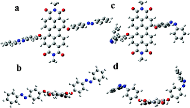 | ||
| Scheme 1 The energy-optimized molecular structure of AZO-PDI with the trans-conformation (E-AZO-PDI) in (a) top view, (b) side view; and the cis-conformation (Z-AZO-PDI) in (c) top view, and (d) side view. | ||
Experimental
Chemicals
Unless stated otherwise, all reagents and anhydrous solvents were obtained from commercial suppliers (J&K Chemical or TCI) and used without further purification and drying except as noted. Column chromatography (CC) was used: SiO2 (200–300 mesh).Synthesis
Fabrication of nanostructures
30 μL of a chloroform solution of the compound AZO-PDI (10−3 mol L−1) before and after irradiation with 365 nm light for 30 min, respectively, was then injected into 2 mL of methanol in a test tube followed by 1 h of aging, the nanoribbons and nanospheres thus formed accordingly. The aggregates can be transferred and casted onto a copper grid or the silicon-slice surface by pipetting. It is worth mentioning that the morphological change of the nanostructures in the dark can take place in the solution dispersion, but is restricted in solid state, i.e. when casted on substrates such as a copper grid and Si, the morphologies can remain for more than 3 months. This is quite important since it is well known that the thermal reverting back from the cis to the trans isomer is the critical drawback for some applications of the azobenzene derivatives.Structure and optical property characterization
1H NMR spectra were recorded on a Bruker DPX 300 spectrometer (300 MHz) in CDCl3 using the residual solvent resonance of CHCl3 at 7.26 ppm relative to SiO2 as an internal reference. Matrix-assisted laser desorption/ionization time-of-flight (MALDI-TOF) mass spectra were detected on a Bruker BIFLEXIII ultrahigh-resolution. Elemental analyses were performed on an elemental analyzer (Vario EI III). Absorption spectra were measured on a Varian Cary 50 spectrophotometer. Steady-state fluorescence measurements of a CHCl3 and CHCl3/CH3OH combined solution of the AZO-PDI compound were performed on a fluorescence spectrophotometer (Hitachi F-4500) with excitation at a wavelength of 480 nm, and the emission spectrum between 500–700 nm was recorded. Transmission electron microscopy images were recorded on a JEOL-100CX II electron microscope operated at 100 kV. A high-resolution transmission electron microscopy (HR-TEM) measurement was performed with a JEOL-2010 working at 200 kV. Scanning electron microscopy images were obtained on a JEOL JSM-6700F. For TEM and HR-TEM imaging, a drop of sample solution was cast onto a copper grid sprayed with carbon. For SEM imaging, Au (1 to 2 nm) was sputtered onto these grids to prevent charging effects and to improve the image clarity. The atomic force microscopy (AFM) images were obtained by using a Digital Instrument Dimension Icon operating in Scan Ansys mode. The X-ray diffraction data were obtained at beamline BL14B1 of the Shanghai Synchrotron Radiation Facility (SSRF) at a wavelength of 1.2398 Å. BL14B1 is a beamline based on a bending magnet, and a Si(111) double crystal monochromator was employed to monochromatize the beam. The size of the focus spot is about 0.5 mm and the end station is equipped with a Huber 5021 diffractometer. NaI scintillation detector was used for data collection. All calculations were carried out with the density functional theory (DFT) method at the B3LYP/6-31G* level. All of the calculations were performed using Gaussian 09 program9 at the Shandong Province High Performance Computing Centre.Electrochemistry measurement
Cyclic voltammograms (CV) were performed in a three-electrode cell using platinum electrodes as a working electrode and a Ag/Ag+ (0.1 M of AgNO3 in acetonitrile) as a reference electrode in an anhydrous and nitrogen-saturated solution of 0.1 M tetrabutylammonium perchlorate (Bu4NClO4) in CH2Cl2 on a CH2-660D electrochemical workstation.Conductivity measurement
The electrical conductivity characterization of the nanoribbons was based on direct current–voltage (I–V) measurement, which was performed with a two-electrode device using Keithley 4200 SCS. Appropriate amounts of nanoribbons were deposited by drop-casting on a silicon wafer covered with a 400 nm thick SiO2 dielectric layer, followed by air-drying in the dark. The gold electrodes were thermally evaporated by mask method onto the nanoribbons. The current measurements were performed in dark. A UV lamp (JiHui, 6W) was used as the UV light source.Results and discussion
Injecting the concentrated chloroform solution of AZO-PDI and that after a long exposure to UV-light into methanol respectively, molecules underwent aggregation due to the limited solubility in methanol, as evidenced from the dramatic changes in the UV-visible spectroscopy. The time dependent absorption spectra of the colloidal dispersions are demonstrated in Fig. 1. The discrepancy between the aggregates obtained from the E- and Z-form isomers can be characterized mainly from the changes of the strong band of the AZO units in the lower wavelengths region. As shown in Fig. 1, compared with the absorption of individual molecules, the maximum absorption of the aggregates at higher wavelengths (the vibronic transitions of the PDI core) obtained from both the E- and Z-isomers decreased along with a blue shift, and accompanied a loss of the fine structure. These features typically suggest the formation of face-to-face π stacks of the adjacent PDI chromophores,5b,10 and the stacking may be relatively compact within the assembly of the E-isomer. Distinct absorption changes are observed in the higher energy region, corresponding to the π–π* transition of the AZO arms. With respect to the aggregated species of the E-isomer, a slight red shift with concomitant absorbance increasing (relative to the absorption of PDI part) is observed in the stationary state compared with the molecularly dissolved species (Fig. 1a). According to the exciton theory,11 this clearly suggests the head-to-tail configuration (J-type manner)12 and pronounces intermolecular facial interaction between a starting dimeric structure of AZO chromophores. On the contrary, as for the absorption of the aggregates of Z-isomer (Fig. 1b), π–π* transition of AZO arms exhibits ambiguous change upon aggregation, indicative of the relative weak interaction between the AZO arms. Accordingly, the sharp peaks in the XRD measurement shown in Fig. 4a (see below) also indicates that the stacking between the AZOs was disordered completely. The AZO moieties may intersect randomly within the aggregates, which is reasonable since the photoisomerization may induce diversified configurations of the AZO arms. Moreover, photo-induced switching behaviour of the assemblies was observed by monitoring the π–π* transition of AZO arms as shown in Fig. S4.† When the aggregates suspension of E-AZO-PDI was irradiated with 365 nm light for time, the absorbance in the higher energy region decreased with hypochromatic shift, implying the molecular conformation transformation within the assemblies.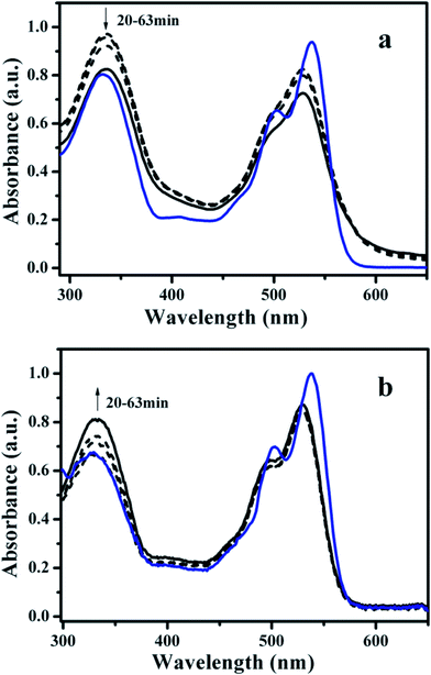 | ||
| Fig. 1 UV-visible absorption spectra of the monomeric AZO-PDI in CHCl3 (10−5 mol L−1) and the time-dependent self-assembled nanostructures formed in CHCl3/CH3OH binary solvents (10−5 mol L−1) at 26 °C. (a) Monomeric E-AZO-PDI (blue line), the self-assemblies formed along with the equilibrium time (black dashed line from top to bottom: 20, 30, 45 min) and the colloidal dispersion at the equilibrium state (black solid line: 63 min); b) monomeric Z-AZO-PDI (blue line), the self-assemblies formed along with the equilibrium time (black dashed line from bottom to top: 20, 30, 45 min) and the colloidal dispersion at the equilibrium state (black solid line: 63 min). | ||
Photo-controlled self-assemble behaviours and the influence of the AZO substitution on the aggregation structure of PDI were subsequently investigated in the solid state. After the CHCl3/CH3OH (v/v = 3/200) binary solution of AZO-PDI (and that upon UV irradiation) equilibrated at 26 °C for more than 1 h, one drop of the solution was evaporated on the carbon-coated grid to observe the morphology of the aggregated species. As shown in Fig. 2a, scanning electron microscopy (SEM) image of the E-AZO-PDI molecular self-assembly depicts well-defined nanoribbons (NRs) bundled together with length of tens of micrometres, as well as quite uniform morphology in terms of both width and thickness, indicating the favourable π–π stacking between the molecules. The aspect ratio of the NRs (length over width) is in a magnitude of 100, and the thickness measured from the twisted cross-section of the NRs in small-area SEM imaging is ca. 30–50 nm (inset in Fig. 2a and S5a†). It is noted that, the 1D nanostructures with controllable size and morphology, including the ribbons, wires, belts or tubes, fabricated from the ordered stacking of the planar π-conjugated molecules are desirable for nanoscale optoelectronic applications, and a lot of recent research has been carried out in an attempt to design and construct the well-defined organic 1D nanostructures deliberately.13 The NRs morphology was also evidenced by the TEM imaging, as shown in Fig. 2b. As seen from the end of each NRs, it is clear that the ribbons are formed through layer-by-layer stacking (inset in Fig. 2a,b, and S5b†). The spacing between each two layers in one ribbon measured from the HR-TEM image is about 15 Å (Fig. S5b†), corresponding well with that observed from the X-ray diffraction (XRD) pattern (see below).
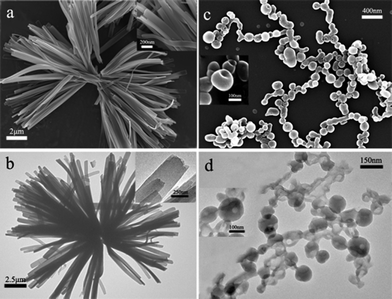 | ||
| Fig. 2 SEM and TEM images of self-assembled nanostructures of AZO-PDI. Nanoribbons formed from E-AZO-PDI in CHCl3/CH3OH observed by (a) SEM and (b) TEM; nano-scale hollow spheres with holes formed from Z-AZO-PDI (obtained by exposure of E-AZO-PDI to 365 nm photoirradiation for more than 30 min) observed by (c) SEM and (d) TEM. | ||
In contrast, SEM observation of the Z-AZO-PDI molecular self-assembly (Fig. 2c) demonstrates approximately spherical-shape nanoparticles that adhered randomly, with an average size of ca. 150 nm and some little holes in their surface. The dimension of the nanospheres (NSs) is rather small in contrast with that of the NRs, and the spherical morphology is consistent with the distorted π–π stacking, which prevents the molecules from assembling along one dimension. The hole is speculated to be formed as the result of etching or dissolution and a decrease in the bending energy.14 The average diameter of the hole is ranging from 20 to 50 nm, as confirmed by the TEM image (Fig. 2d). Such nanospheres with a single hole are expected to be nanocontainers that are capable to encapsulate and release guest solutes on demand controlled by light irradiation, which are of particular interest for cargo delivery.15
The TEM diffraction spots of the single NR (Fig. S5c†) indicate that the NR is crystalline. With an aim to determine the molecular packing and crystallographic orientation of the molecules along individual NRs, we have obtained belt-like single-crystals of one millimetre in length under similar growth conditions as for bulk NRs. The structural parameters were determined for the monoclinic unit cell (C2): a = 33.896 Å, b = 14.787 Å, c = 10.379 Å, β = 92.87°. According to the Bragg's law, the d-spacing (dhkl) can be calculated by using the measured diffraction angle as listed in Table 1.
| Exptl Bragg peak/Å | Calcd Bragg peak/Å | Miller indices | Exptl Bragg peak/Å | Calcd Bragg peak/Å | Miller indices |
|---|---|---|---|---|---|
| 17.19 | 17.13 | (200) | 8.95 | 8.57 | (400) |
| 14.6 | 14.26 | (010) | 5.74 | 5.71 | (600) |
| 13.22 | 13.16 | (110) | 4.31 | 4.28 | (800) |
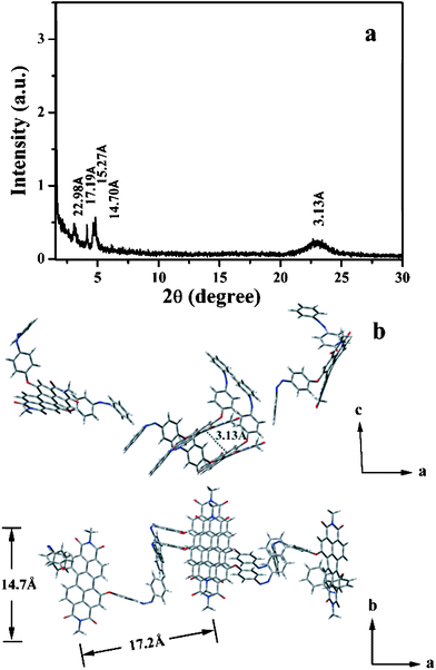
The molecular packing and crystallographic orientation of AZO-PDI molecules within the nanostructures in different morphologies, i.e., NRs and NSs, were further investigated by X-ray diffraction (XRD). The well-defined, sharp peaks shown in the XRD pattern of the NRs (Fig. 3a) are indicative of a layered and crystalline structure of the NRs. The identification of the a axis is rather clear with the nicely spaced reflections. Notice that, the reflections (100), (300), etc. may vanished because of the extinction of the centered lattice according to the X-ray crystallography parameters. The experimental and calculated primary Bragg peaks and the corresponding Miller indices are presented in Table 1. According to the unit cell parameter and the dimension of a single molecule (calculated by DFT, B3LYP/6-31G*), the sharp d-spacing of 17.19 Å corresponds to the distance between the centroid of two neighboring molecules as demonstrated in Fig. 3b. Since when all the AZO arms of a molecule are in trans-station, the overall length of the molecule is about 24.3 Å while the largest d-spacing is 44.09 Å which is smaller than 2 × 24.3 = 48.6 Å, thus the AZO arms of the neighbour molecules must be interdigitated. It is hereby proposed that two AZO-PDI molecules stacked together by π–π interactions between the AZO arms to form a dimer as the building block, further assembles into NRs. According to the HR-TEM observation which shows the well-defined layered structure with spacing of about 15 Å (Fig. S5b†), a d-spacing of 14.6 Å is unambiguously comes from the diffraction of the (010) surface, corresponding well with the b axis within the unit cell and clearly revealing the space between the layers of aligned E-AZO-PDI molecules. The quite sharp peak with a d-spacing of 2.82 Å reveals strong hydrogen-bonding within the assembled structures,16 which may formed between the C![[double bond, length as m-dash]](https://www.rsc.org/images/entities/char_e001.gif) O of the PDI and the H of the AZO as suggested in Fig. 3b. Also in the wide angle region, the typical π–π stacking peak (with d-spacing of about 3.1 Å) denoting the strong interactions between the PDI scaffolds was observed, which is usually found in the 1D nanostructures of PDI derivatives,17 indicating that the extended nanoribbon is dominated by the π–π interaction between the cofacially stacked perylene cores. Consequently, the overlap of the molecular π orbitals, which is crucial for the charge transport in organic semiconductor materials,18 is significant only in the long belt direction (c axis). In this manner, the framework of the 1D nanoribbon is firmed by the synergic action of the π–π stacking and H-bonding to form the long-range ordered and layered structure. A structural model for the intermolecular ordering is presented in Fig. 3b.
O of the PDI and the H of the AZO as suggested in Fig. 3b. Also in the wide angle region, the typical π–π stacking peak (with d-spacing of about 3.1 Å) denoting the strong interactions between the PDI scaffolds was observed, which is usually found in the 1D nanostructures of PDI derivatives,17 indicating that the extended nanoribbon is dominated by the π–π interaction between the cofacially stacked perylene cores. Consequently, the overlap of the molecular π orbitals, which is crucial for the charge transport in organic semiconductor materials,18 is significant only in the long belt direction (c axis). In this manner, the framework of the 1D nanoribbon is firmed by the synergic action of the π–π stacking and H-bonding to form the long-range ordered and layered structure. A structural model for the intermolecular ordering is presented in Fig. 3b.
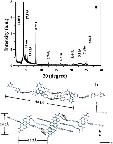 | ||
| Fig. 3 (a) XRD profile of the nanoribbions; (b) schematic illustration of the aggregation mode by four AZO-PDI molecules in the trans-configuration. | ||
With regard to the NSs, the order of the structure reduced apparently from the XRD observation (Fig. 4a). However, π–π stacking at d-spacing of 3.1 Å was still remained while that of 2.8 Å disappeared, indicating PDI cores stack orderly while the intermolecular H-bonds are broken induced by the randomly twisting of the AZO arms. The bending arms not only induced curved structure of the whole molecule, but weakened the interactions between the layers within the ribbons by breaking the intermolecular H-bonds, leading to the spherical morphology. The proposed structure model is illustrated in Fig. 4b. The morphology changes from nanoribbons to nanospheres and the corresponding alternation of the molecular arrangement within the nanostructures are therefore originating from the photo-switching of the AZOs chromophores.
Morphological changes of photoreactive self-assembled nanostructures upon exposure to the light (365 nm and >500 nm respectively) irradiation can be clearly revealed from the atomic force microscopic (AFM) images. The {100} surface of the NRs was measured to determine the morphological changes as represented in Fig. 5. Before photoirradiation, the surface was relatively flat (Fig. 5a). While upon irradiation for more than 2 min with 365 nm light, steps appeared on the surface and the step height increased with prolonging of the irradiation time (Fig. 5b and 5c). The steps with a height of about 1.3 ± 0.1 nm are discerned after the induction period of irradiation, which is supposed to be one layer of the NR (∼1.46 nm, Fig. 3b). The step became indistinct again by bleaching upon irradiation with light (>500 nm) (Fig. 5d). According to the geometrical structure of the molecular arrangements in the NRs obtained from the XRD analysis, bending deflection of the AZO arms breaks the π–π interaction between the benzene rings of the AZOs groups as well as the hydrogen-bonding along the b axis (Fig. 3b and 4b), namely it breaks the lamellar structures formed within the NRs. The rather weak interactions between the PDI cores along the b axis possibly induces the step formation. The reversible surface morphological changes derived by light have also been observed and recorded for a photochromic diarylethene single crystal,19 which is expected to be applied to photodriven nanoscale actuators that reversibly change thickness stepwise by alternate irradiation with UV and visible light.
 | ||
| Fig. 4 (a) XRD profile of the nanospheres; (b) schematic illustration of the aggregation mode by four AZO-PDI molecules in the cis-configuration. | ||
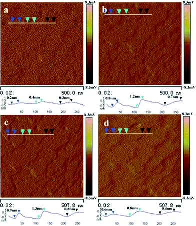 | ||
| Fig. 5 AFM images of the {100} surface of a single nanoribbon exposure to 365 and >500 nm light irradiation, respectively. (a) Top view of the original surface and the sectional view (blue line) of the relative flat surface; (b) Top view of the surface and the sectional view (blue line) of multisteps formed by 365 nm light irradiation for 2 min. (c) Top view of the surface and the sectional view (blue line) of steps formed by 365 nm light irradiation for 10 min. (d) Top view of the surface and the sectional view (blue line) of the relative flat surface after irradiation with light (λ > 500 nm) for 90 min. | ||
All these experimental observations are strongly supportive of the molecular arrangement alternation and morphology transformation of the self-assembly process controlled by light. Consequently, the conductivity of the nanoaggregates is expected to be controlled facilely.
Current–voltage (I–V) curves were recorded over the nanoaggregates deposited on the Si substrates with Au as electrodes. Single NR bridges between the electrodes while the NSs lay out on the electrodes as demonstrated in the microscope images (Fig. 6 and Fig. S7†). For a pristine NR that after irradiation at 365 nm and then upon exposure to the light >500 nm, typical I–V curves (as the function of time) are presented in Fig. 6 and Fig. S6.† As the result of the efficient charge transport via the oriented electron transfer within the 1D molecular arrangement, a nice conductance is determined for the pristine NR irrespective of the bias polarity, with the value of about 2 × 10⁻⁵ S m−1 in air. The current response is dramatically decreased upon exposure to 365 nm irradiation before the stationary state and then nearly returned to the initial value after irradiation with the light >500 nm for 60 s (Fig. S6†), while the NSs fabricated from the Z-isomer demonstrated negligible photocurrent response (Fig. S7†). All the measurements reported here were from a single sample for internal consistency, but they are representative of similar results obtained on several samples. Detailed studies with both experimental and theoretical methods are being carryied out to determine the most important factors that influence the electrical behavior of the assemblies, including the intrinsic conductance switching of the molecule associated with changes in the electronic structure of the molecular junction, and the molecular orientation within the assemblies.
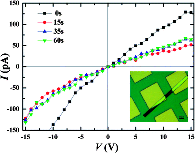 | ||
| Fig. 6 I–V curves for the nanoribbons of AZO-PDI under 365 nm light irradiation along with time. Inset: microscope image showing a single nanoribbion bridging the 20 μm gap between the electrodes (yellow). | ||
Conclusions
The light-controlled fabrication of nanostructures is demonstrated. Perylene diimides decorated with two photo responsive azobenzene moieties in the bay-positions can self-assemble into uniform nanoribbons, while by applying UV irradiation to switch the molecular structure from trans- to cis-form, nanospheres are readily obtained. A single nanoribbon exhibits conductance switching upon photo-induced molecule configurational changes. The nanoribbon, self-assembled from E-AZO-PDI and within which the molecular building blocks are arranged in a high order, shows typical semiconductor properties with good conductance. Along with 365 nm light irradiation, accompany the photoisomerization, conductance decreased gradually and for the nanospheres that were obtained from the Z-isomers, no conductivity is observed. These results allow us to envision these molecules as building blocks for solid-state molecular switch and memory devices with conductance switching.Acknowledgements
This work was supported by National Natural Science Foundation of China (grant nos. 50721002, 51021062, 50990061), the 973 Program of the People's Republic of China (grant no. 2010CB630702), NSFC (21001068), Shandong Province Science Foundation for Excellent Youths (BS2009CL054), and NSFC (20520120221). We thank Dr Hengjiang Cong for his help with the X-ray single-crystal diffraction measurement.References
- (a) R. L. Carroll and C. B. Gorman, Angew. Chem., Int. Ed., 2002, 41, 4378 CrossRef; (b) C. Joachim, J. K. Gimzewski and A. Aviram, Nature, 2000, 408, 541 CrossRef CAS.
- J. E. Green, J. W. Choi, A. Boukai, Y. Bunimovich, E. Johnston-Halperin, E. DeIonno, Y. Luo, B. A. Sheriff, K. Xu, Y. S. Shin, H. R. Tseng, J. F. Stoddart and J. R. Heath, Nature, 2007, 445, 414 CrossRef CAS.
- (a) R. P. Feynman, Eng. Sci., 1960, 23, 22 Search PubMed; (b) R. P. Feynman, Saturday Review, 1960, 23, 45 Search PubMed.
- (a) M. M. Russew and S. Hecht, Adv. Mater., 2010, 22, 3348 CrossRef CAS; (b) S. Yagai, T. Karatsu and A. Kitamura, Chem.–Eur. J., 2005, 11, 4054 CrossRef CAS; (c) C. J. Barrett, J.-i. Mamiya, K. G. Yager and T. Ikeda, Soft Matter, 2007, 3, 1249 RSC.
- (a) L. N. Lucas, J. v. Esch, R. M. Kellogg and B. L. Feringa, Chem. Commun., 2001, 759 RSC; (b) E. H. A. Beckers, S. C. J. Meskers, A. P. H. J. Schenning, Z. J. Chen, F. Wurthner, P. Marsal, D. Beljonne, J. Cornil and R. A. J. Janssen, J. Am. Chem. Soc., 2006, 128, 649 CrossRef CAS.
- (a) C. Wang, Q. S. Chen, H. P. Xu, Z. Q. Wang and X. Zhang, Adv. Mater., 2010, 22, 2553 CrossRef CAS; (b) L. L. Ma, Q. B. Wang, G. F. Lu, R. P. Chen and X. Sun, Langmuir, 2010, 26, 6702 CrossRef CAS; (c) Y. Feng and W. Feng, Opt. Mater., 2008, 30, 876 CrossRef CAS; (d) Y. Y. Lin, X. H. Cheng, Y. Qiao, C. L. Yu, Z. B. Li, Y. Yan and J. B. Huang, Soft Matter, 2010, 6, 902 RSC.
- (a) E. S. Tam, J. J. Parks, W. W. Shum, Y. Zhong, M. E. B. S. Berrıos, X. Zheng, W. Yang, G. K.-L. Chan, H. D. Abruna and D. C. Ralph, ACS Nano, 2011, 5, 5115 CrossRef CAS; (b) X. Zhang, J. Jie, W. Zhang, C. Zhang, L. Luo, Z. He, X. Zhang, W. Zhang, C. Lee and S. Lee, Adv. Mater., 2008, 20, 2427 CrossRef CAS; (c) J. M. Mativetsky, G. Pace, M. Elbing, M. A. Rampi, M. Mayor and P. Samorì, J. Am. Chem. Soc., 2008, 130, 9192 CrossRef CAS; (d) S. Das, S. Varghese and N. S. S. Kumar, Langmuir, 2010, 26, 1598 CrossRef CAS; (e) H. Cao, J. Jiang, X. Zhu, P. Duan and M. Liu, Soft Matter, 2011, 7, 4654 RSC.
- (a) K. Balakrishnan, A. Datar, T. Naddo, J. Huang, R. Oitker, M. Yen, J. Zhao and L. Zang, J. Am. Chem. Soc., 2006, 128, 7390 CrossRef CAS; (b) K. Balakrishnan, A. Datar, R. Oitker, H. Chen, J. Zuo and L. Zang, J. Am. Chem. Soc., 2005, 127, 10496 CrossRef CAS.
- R. A. Cox, Gaussian 09, Gaussian, Inc., Wallingford CT, 2009 Search PubMed.
- (a) Z. Chen, U. Baumeister, C. Tschierske and F. Würthner, Chem.–Eur. J., 2007, 13, 450 CrossRef CAS; (b) S. Ghosh, X.-Q. Li, V. Stepanenko and F. Würthner, Chem.–Eur. J., 2008, 14, 11343 CrossRef CAS.
- (a) K. Ariga, Y. Lvov and T. Kunitake, J. Am. Chem. Soc., 1997, 119, 2224 CrossRef CAS; (b) N. C. Maiti, S. Mazumdar and N. Periasamy, J. Phys. Chem. B, 1998, 102, 1528 CrossRef CAS.
- (a) T. Fujii, H. Kashida and H. Asanuma, Chem.–Eur. J., 2009, 15, 10092 CrossRef CAS; (b) K. S. Kumar and A. Patnaik, Chem.–Eur. J., 2011, 17, 5327 CrossRef CAS; (c) E. G. M. a. M. Kasha, J. Chem. Phys., 1958, 28, 721 CrossRef; (d) H. R. R. a. M. A. E.-B. M. Kasha, Pure Appl. Chem., 1965, 11, 371 CrossRef.
- (a) L. Zang, Y. Che and J. S. Moore, Acc. Chem. Res., 2008, 41, 1596 CrossRef CAS; (b) F. Würthner, Chem. Commun., 2004, 1564 RSC.
- D. Li and Y. Zheng, J. Org. Chem., 2011, 76, 1100 CrossRef CAS.
- Y. Wang, P. Han, H. Xu, Z. Wang, X. Zhang and A. V. Kabanov, Langmuir, 2010, 26, 709 CrossRef CAS.
- (a) Y. Liu, J. Ding, D. Shi and J. Sun, J. Phys. Chem. A, 2008, 112, 6244 CrossRef CAS; (b) K. Kobayashi, A. Sato, S. Sakamoto and K. Yamaguchi, J. Am. Chem. Soc., 2003, 125, 3035 CrossRef CAS; (c) S. D. Feyter, A. Miura, S. Yao, Z. Chen, F. Wurthner, P. Jonkheijm, A. P. H. J. Schenning, E. W. Meijer and F. C. D. Schryver, Nano Lett., 2005, 5, 77 CrossRef.
- (a) C. W. Struijk, A. B. Sieval, J. E. J. Dakhorst, M. van Dijk, P. Kimkes, R. B. M. Koehorst, H. Donker, T. J. Schaafsma, S. J. Picken, A. M. van de Craats, J. M. Warman, H. Zuilhof and E. J. R. Sudholter, J. Am. Chem. Soc., 2000, 122, 11057 CrossRef CAS; (b) Y. Che, A. Datar, K. Balakrishnan and L. Zang, J. Am. Chem. Soc., 2007, 129, 7234 CrossRef CAS; (c) Y. K. Che, X. M. Yang, G. L. Liu, C. Yu, H. W. Ji, J. M. Zuo, J. C. Zhao and L. Zang, J. Am. Chem. Soc., 2010, 132, 5743 CrossRef CAS.
- A. L. Briseno, S. C. B. Mannsfeld, C. Reese, J. M. Hancock, Y. Xiong, S. A. Jenekhe, Z. Bao and Y. Xia, Nano Lett., 2007, 7, 2847 CrossRef CAS.
- M. Irie, S. Kobatake and M. Horichi, Science, 2001, 291, 1769 CrossRef CAS.
Footnote |
| † Electronic Supplementary Information (ESI) available: Synthesis, I–V, spectroscopy, and microscopy measurements. See DOI: 10.1039/c2ra00816e/ |
| This journal is © The Royal Society of Chemistry 2012 |