Sub-40 nm polymer dot arrays by self-organized dewetting of electron beam treated ultrathin polymer films
Ankur
Verma
and
Ashutosh
Sharma
*
Department of Chemical Engineering and DST Unit on Soft Nanotechnology, Indian Institute of Technology Kanpur, Kanpur, UP, India 208016. E-mail: ashutos@iitk.ac.in; Fax: +91-512-259-0104; Tel: +91-512-259-7026
First published on 7th February 2012
Abstract
Sub-40 nm size ordered nanodroplet arrays of polystyrene are fabricated by a low dose selective electron beam exposure of an ultrathin polymer film followed by its intensified self organized dewetting under a mixture of water and polar organic solvents. The self organization speeds up patterning and reduces the feature size, both by more than 10 times.
Fabrication of nanopatterned and functionalized polymeric surfaces is an active area owing to its many important applications in the areas of nanophotonics, nanoelectronics, and templated synthesis of nanostructured materials.1 There are several mature technologies for the nano-fabrication of soft surfaces, mainly dominated by extreme UV and X-ray photolithography, nano-imprint lithography (NIL) and electron beam lithography (EBL).2 However, photolithography suffers from diffraction limit and to create structures of size less than 50 nm requires complicated multistep process, interferometry and the whole system to be immersed in high refractive index liquid.3NIL, on the other hand, is a single step process and can replicate patterns of a size as small as 20 nm but it requires a master to be fabricated first by some other technique.4EBL is a serial writing process which is considered slow for large area nanopatterning. Scanning probe techniques such as dip pen nanolithography, although are capable of manipulating individual atoms and can achieve molecular resolution in patterning, but are not particularly scalable.5 The quest for miniaturization with affordability continuously motivates the need for better and faster tools of nanofabrication.6 Here we combine low dose EBL with directed instability of ultrathin polymer films to fabricate arrays of polymer nanodots by self-organization, the latter speeds up the fabrication by more than 10 times compared to conventional EBL.
The bottom up approach such as physical or chemical self-assembly can significantly reduce the fabrication cost and time by replacing high-end fabrication tools either completely or partially.7 Simultaneously, these methods also provide one step solution for the fabrication of smooth or complex 3D structures. Self-organized dewetting of ultrathin (<100 nm) polymer films when coated on a non-wetting substrate, is one of the possible bottom up approach to combine with a top down method to enhance its usability and performance. Thin film dewetting has been an active research field during the last two decades leading to several interesting solutions for the micropatterning of soft surfaces.8 However, it has been limited to the patterns of micrometre size or more because of the limitations imposed by high surface tension, which opposes the creation of a new surface, and the weak destabilizing van der Waals potential. Recent developments9 in the self organized dewetting of polystyrene films have enabled the fabrication of submicrometer size (∼200 nm) droplets by overcoming the limitations of strong interfacial tension and weak destabilizing van der Waals potential. The dewetting under a mixture of water and polar organic solvents reduces the interfacial tension by more than one order and also introduces a stronger destabilizing electrostatic potential.9 Another limitation of dewetting on a homogeneous and flat substrate is that it produces droplets with wide size distribution and they are randomly distributed on the substrate. To overcome these limitations, various strategies such as dewetting on physico-chemically patterned surfaces9,10 and e-beam modified films11 have been proposed. The initial patterning of substrates, however, requires a top down fabrication method such as optical lithography and the removal of pre-pattern after dewetting is to be done by selective lift-off or etching, both of which limit the usefulness and flexibility of the template method.9,10 Modification of polymer films by EBL followed by dewetting does not leave behind any signature of the pre-pattern and hence suitable for direct applications. The basic idea behind this is to create a differential of polymer viscosity by low dose EBL so as to localize the nucleation of dewetting by changing the growth rate of instability. It was thus possible to fabricate ∼100 nm polystyrene nano-droplets with the periodicity of 220 nm using this strategy.11
We show here that an optimized low dose EBL/dewetting process can push down the limits of patterning to true nano-domain. We demonstrated the method by fabrication of nano-arrays of less than 40 nm domain size and 100 nm periodicity. It was achieved on a 5.2 nm thick polystyrene (PS, Mw = 280 kg mol−1) film coated on a thoroughly cleaned silicon wafer with a native oxide layer. The PS thin film was exposed to an extremely low dose of e-beam by using a field emission scanning electron microscope (FESEM, Zeiss Supra 40 V) coupled to a pattern generator (XENOS XeDraw 2) to produce a square grid of single pixel lines with 100 nm period (Fig. 1a). Points along a line at separation of 10 nm were exposed with 0.05 fC of e-beam dose (250 pA beam current, 200 ns dwell time). Therefore, the e-beam dose used in this experiment was 50 pC cm−1. When perfectly focused, the spot size of e-beam was 4 nm in the exposure area of 200 × 200 μm2. The e-beam dose was optimized on two conflicting factors: large doses increased the patterning time and the feature size by lateral dispersion, whereas too low doses do not produce enough viscosity contrast for a clearly defined differential dewetting. Dewetting of e-beam exposed film was carried out by immersing it in a mixture of water and polar organic solvents (water, methyl ethyl ketone and acetone in the ratio 15![[thin space (1/6-em)]](https://www.rsc.org/images/entities/char_2009.gif) :7:3).9 The solvent molecules diffuse into the polymer film and bring down its glass transition temperature below room temperature thus allowing dewetting at room temperature, while water being majority phase prevents the solubilization of polymer in the dewetting mixture. The dewetting mixture greatly intensifies dewetting by reducing interfacial tension and switching to electrostatic destabilizing potential, which allows dewetting to happen extremely quickly (<1 s for PS films thinner than 10 nm). In case of 5.2 nm thick PS film the dewetting is completed almost instantaneously. Therefore nucleation or growth rate for instability could not be accurately measured in these experiments. PS exhibits higher viscosity in the e-beam exposed regions, i.e., it acts as a negative tone e-beam resist.11 This results in the faster growth of instabilities in the unexposed regions (Fig. 1b) leading to the formation of a grid like pattern corresponding to the e-beam exposed high viscosity areas (Fig. 1c). The square grid eventually breaks up to form droplets at the intersection points (Fig. 1d). Once the dewetting is complete the samples can be removed from the dewetting mixture and dried in the stream of hot air, which solidifies the nanostructures and make them permanent.
:7:3).9 The solvent molecules diffuse into the polymer film and bring down its glass transition temperature below room temperature thus allowing dewetting at room temperature, while water being majority phase prevents the solubilization of polymer in the dewetting mixture. The dewetting mixture greatly intensifies dewetting by reducing interfacial tension and switching to electrostatic destabilizing potential, which allows dewetting to happen extremely quickly (<1 s for PS films thinner than 10 nm). In case of 5.2 nm thick PS film the dewetting is completed almost instantaneously. Therefore nucleation or growth rate for instability could not be accurately measured in these experiments. PS exhibits higher viscosity in the e-beam exposed regions, i.e., it acts as a negative tone e-beam resist.11 This results in the faster growth of instabilities in the unexposed regions (Fig. 1b) leading to the formation of a grid like pattern corresponding to the e-beam exposed high viscosity areas (Fig. 1c). The square grid eventually breaks up to form droplets at the intersection points (Fig. 1d). Once the dewetting is complete the samples can be removed from the dewetting mixture and dried in the stream of hot air, which solidifies the nanostructures and make them permanent.
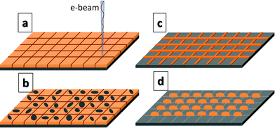 | ||
| Fig. 1 Schematic diagram of e-beam exposure pattern and dewetting. (a) Polymer film is exposed to e-beam in a square grid pattern. (b) Dewetting starts with the formation of holes in the unexposed area. (c) Holes grow in size and allow polymer to get accumulated along the high viscosity (exposed) regions. (d) The square grid of polymer eventually breaks up to form droplets at the intersection points. | ||
The initial thickness of the polymer film governs the spinodal length scale of dewetting, i.e. the average spacing between the droplets in case of dewetting of homogeneous (unexposed) film.9,11 The alignment of dewetted patterns in e-beam exposed film is best when the e-beam pattern periodicity is close to the spinodal length scale for that particular film thickness. A 5 nm thick PS film without e-beam exposure dewets under the mixture to produce droplets of size 48 ± 18 nm at a mean separation of 156 ± 37 nm (Fig. 2a). Fig. 2b shows the FESEM image of an ordered array of 35 ± 7 nm droplets of polystyrene with 100 nm periodicity fabricated by this method. The e-beam exposure of 1 mm2 area took about 200 s, and produced ordered array of 10000 × 10000 nano-droplets upon dewetting (0.5 million nanodroplets per second). This is significantly faster than the conventional EBL and thus takes a leap forward in using e-beam for large area nano-patterning.
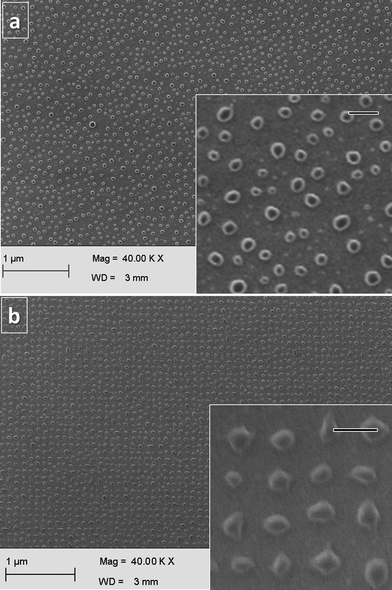 | ||
| Fig. 2 PS nano-droplets produced by the self-organized dewetting of 5.2 nm thick polymer film. (a) Randomly distributed PS nano-droplets produced by dewetting of unexposed film have mean diameter of 48 ± 18 nm and mean separation of 156 ± 37 nm. (b) Ordered PS nano-droplets by dewetting of e-beam exposed film have mean diameter of 35 ± 7 nm arranged in a 100 nm array over a large area (200 μm × 200 μm). Inset shows the magnified view of nano-droplets. Scale bar: 100 nm (inset). | ||
Based on the molecular weight, size of one PS molecule is about 14 nm.12 Thus, there are about 10 molecules of PS in a 35 nm droplet. This, together with the propensity for the contact line pinning in small dimensions, are the possible reasons for somewhat irregular shapes of these very small droplets. Such droplets become nearly spherical owing to the surface tension in larger diameters >100 nm. The droplet sizes obtained here represent the limit of the self-organized dewetting because initially smooth, uniform films of PS thinner than 5 nm could not be spin coated. This thickness is likely the limit of the highly constrained monolayer coverage. On the other hand, low molecular weight polymers (PS and PMMA) do not show sufficient viscosity contrast after short e-beam exposures. Moreover, the dewetting kinetics is also much faster for low molecular weight polymer thin-films. This eventually leads to the more disorder in the dewetted patterns and thus, low molecular weight polymers are not found to be suitable candidates for e-beam assisted patterning.
Considering this limitation, we believe that this is close to the minimum possible feature size that can be fabricated by the self-organized dewetting of thin viscous polymer films. It may also be noted that the directed dewetting of liquid polymer films under the solvent–nonsolvent mix demonstrated here is entirely different from the very slow instability of solid polymer films in a non-solvent like water.13
The hybrid method proposed is particularly useful for the fabrication of nanolens arrays,8 photonic crystals14 and engineered surfaces with selective wettability and structural colors.15 In particular, smooth profiles such as in lenses, cannot be fabricated easily and inexpensively by the top-down methods like EBL and FIB. The method also has the advantage for the positioning of functional materials such as catalyst nanoparticles (e.g., gold, silver, iron) in regular arrays by embedding them in the polymer film and subsequent selective removal of the polymer by thermal decomposition or other means.16 Such array of catalyzing nanoparticles can be used for the synthesis and growth of aligned and regularly spaced nanowires and nanotubes that find applications in sensors, light emitting diodes and photovoltaic devices.
This report describes a novel method of nano-patterning by a combination of bottom up and top down techniques, which facilitates much faster fabrication of sub-100 nm polymer domains compared to EBL, positioning it as an efficient tool for large area nano-patterning. This is the first demonstration of the fabrication of sub-100 nm polymeric structures by self organized dewetting of polymer thin films. The key to the success of this technique lies in the intensification of dewetting under the water-solvent media. Further, the use of extremely low doses of e-beam induces ordering of nano-droplets, which is more than 10 times faster than the conventional EBL. In conventional EBL, relatively high e-beam exposures (∼10 times) are required to modify the resist completely so that the developer can selectively dissolve one of the regions. However, in the proposed method, only a small e-beam exposure produces enough viscosity contrast that results in the ordered pattern after dewetting. The droplets are arranged along any arbitrary pattern drawn by the e-beam. Finally, the polymer used in the process does not have to be a good e-beam resist material as the process works by creating small differentials of effective viscosity and the kinetics of dewetting in highly confined domains.
Acknowledgements
This work is supported by Department of Science and Technology, Government of India by its Unit on Soft Nanotechnology at IIT Kanpur and an IRPHA grant.References
- (a) G. R. Whittell, M. D. Hager, U. S. Schubert and I. Manners, Nat. Mater., 2011, 10, 176 CrossRef CAS; (b) L. Jiang, X. Wang and L. F. Chi, Small, 2011, 7, 1309 CrossRef CAS; (c) W. Shi, P. F. Liang, D. T. Ge, J. X. Wang and Q. Q. Zhang, Chem. Commun., 2007, 23, 2414 RSC.
- A. del Campo and E. Arzt, Chem. Rev., 2008, 108, 911 CrossRef CAS.
- T. M. Bloomstein, M. F. Marchant, S. Deneault, D. E. Hardy and M. Rothschild, Opt. Express, 2006, 14, 6434 CrossRef CAS.
- H. Schift, J. Vac. Sci. Technol., B: Microelectron. Nanometer Struct.–Process., Meas., Phenom., 2008, 26, 458 CrossRef CAS.
- (a) J. A. Liddle and G. M. Gallatin, Nanoscale, 2011, 3, 2679 RSC; (b) C. C. Wu, D. N. Reinhoudt, C. Otto, V. Subramaniam and A. H. Velders, Small, 2011, 7, 989 CrossRef CAS.
- (a) H. E. Maes, C. Claeys, R. Mertens, A. Campitelli, C. Van Hoof and J. De Boeck, Adv. Eng. Mater., 2001, 3, 781 CrossRef CAS; (b) S. E. Thompson and S. Parthasarathy, Mater. Today, 2006, 9, 20 CrossRef CAS.
- (a) A. M. Hung, H. Noh and J. N. Cha, Nanoscale, 2010, 2, 2530 RSC; (b) K. Ariga, X. L. Hu, S. Mandal and J. P. Hill, Nanoscale, 2010, 2, 198 RSC.
- (a) G. Reiter, Phys. Rev. Lett., 1992, 68, 75 CrossRef CAS; (b) A. Sharma and G. Reiter, J. Colloid Interface Sci., 1996, 178, 383 CrossRef CAS; (c) A. Sharma, Eur. Phys. J. E, 2003, 12, 397 CrossRef CAS; (d) R. Xie, A. Karim, J. F. Douglas, C. C. Han and R. A. Weiss, Phys. Rev. Lett., 1998, 81, 1251 CrossRef CAS; (e) S. Herminghaus, Phys. Rev. Lett., 1999, 83, 2359 CrossRef CAS; (f) R. Seeman, S. Herminghaus and K. Jacobs, Phys. Rev. Lett., 2001, 86, 5534 CrossRef; (g) J. Becker, G. Grun, R. Seemann, H. Mantz, K. Jacobs, K. R. Mecke and R. Blossey, Nat. Mater., 2002, 2, 59 CrossRef; (h) R. V. Craster and O. K. Matar, Rev. Mod. Phys., 2009, 81, 1131 CrossRef CAS; (i) X. Ma, R. Crombez, M. Ashaduzzaman, M. Kunitake, L. Slater, T. Mourey and J. Texter, Chem. Commun., 2011, 47, 10356 RSC; (j) D. Zhao, A. D. Martinez, X. L. Xi, X. L. Ma, N. Wu and T. B. Cao, Small, 2011, 7, 2326 CrossRef CAS; (k) M. Ramanathan and S. B. Darling, Prog. Polym. Sci., 2011, 36, 793 CrossRef CAS.
- (a) A. Verma and A. Sharma, Adv. Mater., 2010, 22, 5306 CrossRef CAS; (b) A. Verma and A. Sharma, Macromolecules, 2011, 44, 4928 CrossRef CAS.
- (a) A. M. Higgins and R. A. L. Jones, Nature, 2000, 404, 476 CrossRef CAS; (b) E. Mayer and H.-G. Braun, Macromol. Mater. Eng., 2000, 276–277, 44 CrossRef; (c) B. Yoon, H. Acharya, G. Lee, H.-C. Kim, J. Huh and C. Park, Soft Matter, 2008, 4, 1467 RSC; (d) R. Mukherjee, D. Bandopadhyay and A. Sharma, Soft Matter, 2008, 4, 2086 RSC; (e) W. Cheng, N. Park, M. T. Walter, M. R. Hartman and D. Luo, Nat. Nanotechnol., 2008, 3, 682 CrossRef CAS; (f) R. Konnur, K. Kargupta and A. Sharma, Phys. Rev. Lett., 2000, 84, 931 CrossRef CAS; (g) K. Kargupta and A. Sharma, Phys. Rev. Lett., 2001, 86, 4536 CrossRef CAS; (h) G. T. Carroll, N. J. Turro and J. T. Koberstein, J. Colloid Interface Sci., 2010, 351, 556 CrossRef CAS; (i) D. Zhu, X. Li, G. Zhang, W. Li, X. Zhang, X. Zhang, T. Wang and B. Yang, Langmuir, 2010, 26, 5172 CrossRef CAS; (j) R. Mukherjee, M. Gonuguntla and A. Sharma, J. Nanosci. Nanotechnol., 2007, 7, 2069 CrossRef CAS; (k) R. Xing, C. Luo, Z. Wang and Y. Han, Polymer, 2007, 48, 3574 CrossRef CAS; (l) K. Khare, M. Brinkmann, B. M. Law, E. L. Gurevich, S. Herminghaus and R. Seemann, Langmuir, 2007, 23, 12138 CrossRef CAS.
- A. Verma and A. Sharma, Soft Matter, 2011, 7, 11119 RSC.
- K. Terao and J. W. Mays, Eur. Polym. J., 2004, 40, 1623 CrossRef CAS.
- (a) I. Siretanu, J. P. Chapel and Carlos Drummond, ACS Nano, 2011, 5, 2939 CrossRef CAS; (b) L. Xu, T. Shi and L. An, Langmuir, 2007, 23, 9282 CrossRef CAS.
- (a) J. Zhang, Z. Sun and B. Yang, Curr. Opin. Colloid Interface Sci., 2009, 14, 103 CrossRef CAS; (b) X. Luo, A. J. Killard, A. Morrin and M. R. Smyth, Chem. Commun., 2007, 30, 3207 RSC.
- (a) O. Sato, S. Kubo and Z. Gu, Acc. Chem. Res., 2009, 42, 1 CrossRef CAS; (b) K. Ueno, A. Inaba, Y. Sano, M. Kondoh and M. Watanabe, Chem. Commun., 2009, 24, 3603 RSC.
- (a) K. A. Barnes, A. Karim, J. F. Douglas, A. I. Nakatani, H. Gruell and E. J. Amis, Macromolecules, 2000, 33, 4177 CrossRef CAS; (b) R. Mukherjee, S. Das, A. Das, S. K. Sharma, A. K. Raychaudhuri and A. Sharma, ACS Nano, 2010, 4, 3709 CrossRef CAS.
| This journal is © The Royal Society of Chemistry 2012 |