Polymer brushes assisted loading of high density CdS/CdSe quantum dots onto TiO2 nanotubes and the resulting photoelectric performance
Junfeng
Yan
ab,
Qian
Ye
a and
Feng
Zhou
*a
aState Key Laboratory of Solid Lubrication, Lanzhou Institute of Chemical Physics, Chinese Academy of Sciences, Lanzhou, 730000, China
bGraduate School, Chinese Academy of Sciences, Beijing, 100039, China. E-mail: zhouf@lzb.ac.cn
First published on 13th March 2012
Abstract
Cadmium sulfide (CdS) and cadmium selenide (CdSe) quantum dots (QDs) are sequentially loaded onto anodized TiO2 nanotubes to fabricate a CdS/CdSe co-sensitized photoelectrode for visible light response. These QDs are loaded on TiO2 nanotubes by polymer brushes assisted in situ formation, and they are distributed uniformly around both inner and outer walls of TiO2 nanotubes. The interpenetrating polymer can provide a superior nano-confined environment and will prevent the nanoparticles from growing further during nucleation. More importantly, the potential advantage of using polymer brushes is the capability of tuning the loading amount of QDs via multiple cation exchange. The photoresponse of CdS/CdSe-TiO2 nanotubes has been efficiently extended into the visible-light region, indicating potential applications in solar cell devices.
1. Introduction
Titanium oxide (TiO2) is one of the most important inorganic materials in fabricating photovoltaic devices such as dye-sensitized solar cells (DSSCs), quantum dots solar cells and TiO2/polymer solar cells.1–7 Among different types of titania nanomaterials, anodized TiO2 nanotubes have attracted widespread interest through being a promising one-dimensional nanostructured material for constructing solar energy conversion assemblies,8 due to their high surface-to-volume ratio available for dye adsorption and their good electronic transmission efficiency.9–11 However, the wider band gap (3.2 eV) of anatase TiO2 limits its photoresponse to the ultraviolet (UV) region and thus hinders the efficient utilization of solar energy. In order to make TiO2 responsive to visible light, many strategies have been proposed, mainly based on photosensitization of TiO2 materials by visible-responsive sensitizers, including dye sensitizing,12 making compounds that include quantum dots,13 and element doping.14Till now, organic dyes have been regarded as one of the most efficient sensitizers for TiO2 materials for solar cells, and the solar cell conversion efficiencies have achieved about 11%.15,16 However, the poor stability and high cost of organic dyes limit their applications. In recent years, quantum dots (QDs) have emerged as a promising candidate that can trigger a wider light absorption range and have potential applications in photovoltaic cells,17 which have opened new approaches to design and fabricate QDs or QDs combinations for promising solar cells efficiencies and for improving the stability of the material. These semiconductor QDs with tunable energy gaps offer new opportunities for solar energy conversion, in which the size quantization effect makes the photoresponse occurr over a wider spectral region via tuning the size of QDs.18 In addition, the quantum confinement effect enables the possibility of generating multiple electron–hole pairs per photon through the impact ionization effect.19 Many methods have been developed to sensitize TiO2 nanotubes (TiO2 NTs) for visible light harvesting, such as chemical bath deposition,20,21 cathodic reduction,22 close space sublimation technique,23 spray pyrolysis deposition,24 organic linker assisted deposition25,26 and electrochemical atomic layer deposition.27 Chemical bath deposition is very popular for generating CdS QDs on TiO2 NTs, a photoelectrochemical cell efficiency of 4.15% has been attained.20 Single CdS QDs can not overlap the entire visible solar spectrum, so CdS and CdSe QDs were both assembled onto nanoparticulated TiO2 films for favoring the separation and transfer of photoinduced electrons and holes, and 4.22% efficiency was attained.28
Surface initiated polymerization can graft polymer brushes onto a wide variety of substrates to prepare functional surfaces.29–33 Polymer brushes can form a nano-confined environment for fabrication of quantum dots, so that their size will be well controlled with uniform distribution.34,35 Directly grafting polymer brushes via surface-initiated polymerization on TiO2 NTs with chemical bonding will provide a superior platform to introduce diverse QDs onto TiO2 NTs, thus we can finely tune the photoresponse properities. Catechol and its derived compounds can self-assemble on various inorganic and organic materials with a good adhesion,36,37 which is an effective approach to modify TiO2 surfaces with polymer chains chemically tethered to an interface. Here, we fabricated a high density polymer brushes modified TiO2 NTs via surface initiated polymerization using catecholic initiator.38–40 Then it was followed by simple gas–solid and liquid–solid reactions to obtain narrow size distributed CdS and CdSe QDs with high coverage on the inner and outer walls of TiO2 NTs, which can be ascribed to the grafted polymer chains that stabilized newly formed QDs and prevented their further collisions, which therefore prevented nucleation. The light absorption of the as-prepared materials was expanded to the visible light region, as shown by photoelectrochemical cell measurements, and these composite materials showed good photocurrent and photovoltage response properties.
2. Experimental
2.1. Reagent
Initiator 2-bromo-2-methyl-N-[2-(3,4-dihydroxy-phenyl)-ethyl]-propionamide was synthesized according to previous studies.41 Copper(I) bromide (CuBr) was purified by reflux in acetic acid. 3-hydroxytyramine hydrochloride was obtained from Aldrich. The ultrapure water used in all experiments was obtained from a NANOpure Infinity system from Barnstead/Thermolyne Corporation. Other reagents were used as received.2.2. Synthesis of monomer cadmium dimethacrylate (Cd(MA)2)
32.1 g CdO, 45 mL methacrylic acid (MA) and 60 mL distilled water were added to a 250 mL flask and the mixture was refluxed for 2 h at 60 °C. Then the product was filtrated and the filtrate was vacuum distilled to remove some water and the unreacted MA, the remainder was cooled and further collected by filtration and recrystallized from ethanol to give white flaky crystals, which are the cadmium dimethacrylate (Cd(MA)2) target product.42 Finally, it was dried in a vacuum oven at room temperature for 24 h.2.3. Substrate preparation, initiator modification and surface-initiated polymerization
Highly ordered TiO2 NTs were prepared by a two-step potentiostatic anodization using commercial Ti foil as the anode, with a graphite slice as the counter electrode. The voltage was applied using a DC power supply (LW10J2, Shanghai). Before anodization, the titanium foils were washed with ethanol and acetone by ultrasonication to remove the oil layer, then washed with distilled water and dried in the air. The first anodization was carried out in ethylene glycol electrolyte containing 0.5 wt% NH4F at 20 °C for about 2 h under a voltage of 60 V, then the TiO2 nanotube films were easily peeled off in 1 M HCl under ultrasonication, resulting in bowl-like footprints on the Ti foil. The second anodization was carried out under the same conditions, with the addition of 0.5% HF in the electrolyte, for about 2 h to obtain highly ordered TiO2 NTs. The as-prepared samples were annealed at 450 °C for 2 h in air to induce crystallinity to obtain anatase TiO2 NTs.43,44The initiator modification process: anodized TiO2 NTs (4.5 cm2) were immersed in 1.5 mg mL−1 solution (ethanol![[thin space (1/6-em)]](https://www.rsc.org/images/entities/char_2009.gif) :distilled water = 1:4) of initiator and stirred for 24 h in the dark under N2 protection at room temperature. The initiator modified TiO2 NTs were washed with distilled water and ethanol.
:distilled water = 1:4) of initiator and stirred for 24 h in the dark under N2 protection at room temperature. The initiator modified TiO2 NTs were washed with distilled water and ethanol.
Surface-initiated polymerization on TiO2 NTs: 2 g Cd(MA)2 monomer and 20 mL distilled water were placed in a flask under N2 flow and stirred for about 30 min to dissolve the monomer, then 60 mg bipyridyl and 30 mg CuBr were charged into the flask under N2 flow, 30 min later the initiator modified TiO2 NTs were added into the monomer solution, the polymerization was performed at 60 °C under N2 protection for 4 h. The polymer-grafted TiO2 NTs (denoted as TiO2 NTs-PMAA-Cd) were taken out of the polymerization solution and washed with distilled water and ethanol, then dried under N2 flow. The whole polymer grafting process on TiO2 NTs is shown in Scheme 1(A).
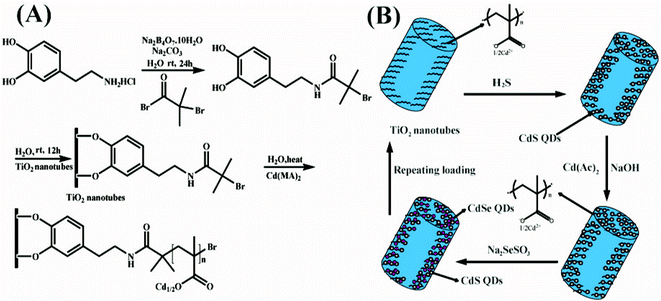 | ||
| Scheme 1 (A) Preparation of polymer brushes grafted TiO2 NTs. (B) Successive loading of CdS/CdSe QDs onto TiO2 NTs. | ||
2.4. Preparation of CdS/CdSe QDs sensitized TiO2 NTs
The polymer brushes grafted TiO2 NTs were put into an evacuated vial and H2S gas was injected into it. The gas–solid reaction was performed for 48 h at room temperature to convert the Cd ions into CdS nanoparticles. For reusing the polymer chains to prepare CdSe nanocrystals, CdS-PMAA-TiO2 NTs were immersed in 30 mL 0.5 M NaOH (methanol as the solvent). After stirring for 12 h, the sample was purified using centrifugation with copious ultrapure water and ethanol, then the Cd ion exchange was carried out in 30 mL 0.5 M Cd(Ac)2 (methanol as the solvent), then CdS-PMAA-Cd-TiO2 NTs were put into Na2SeSO3 solution at 50 °C for 3 h to prepare CdSe/CdS-TiO2 NTs. Sodium selenosulphate (Na2SeSO3) was prepared by refluxing Se (0.3 M) in an aqueous solution of Na2SO3 (0.6 M) at 70 °C for about 7 h.28Scheme 1(B) depicts the fabrication process for CdS/CdSe QDs decorated TiO2 NTs.2.5. Photoelectrochemical tests
Photoelectrochemical measurements were carried out using a two electrode cell system: CdS/CdSe QDs sensitized TiO2 NTs as the photoanode and Pt foil as the counter electrode. The measurements were carried out in 0.1 M Na2S solution as the redox couple, a 150 W xenon lamp was used as the monochromatic light source (SM-25 Hyper Monolight, Japan) and a Keithley 2635A System SourceMeter was used to record the current values, the active area of the photoelectrochemical cell is 0.16 cm2. The photocurrent and photovoltage response measurements were performed at room temperature using a CHI 660B electrochemical workstation (Shanghai, China), a conventional three-electrode cell was used, including a saturated Ag/AgCl electrode (SCE) as the reference electrode, a platinum counter electrode, and CdS and CdSe QDs sensitized TiO2 NTs as the working electrode. The light intensity is 150 mW cm−2 under simulated sunlight and the cell area is also 0.16 cm2.2.6. Characterization
Attenuated total reflection infrared (ATR-IR) spectra were measured using a Nicolet iS10 instrument (Thermo Nicolet Corporation). Chemical composition information about the samples was obtained by X-ray photoelectron spectroscopy (XPS), the measurement was carried out on a PHI-5702 multifunctional spectrometer using Al Kα radiation, and the binding energies were referenced to the C1s line at 284.8 eV from adventitious carbon. The morphology of CdSe/CdS-TiO2 NTs was determined by field emission scanning electron microcopy (JSM-6701F, JEOL Inc., Japan), and energy dispersive spectroscopy (EDS) was also carried out with a FESEM (JSM-6701F), which was used for the cross-sectional elemental analysis of the nanotubes. The phase identification of the samples was conducted with powder X-ray diffraction (XRD) experiments on a RigaKu D/max-RB diffractometer with Ni-filtered graphite-monochromatized Cu-Kα radiation (λ = 1.54056 Å). UV-vis diffuse-reflectance spectra were measured at room temperature using a Lambda 950 UV-vis spectrometer (Perkin Elmer).3. Results and discussion
3.1. ATR-IR spectrum
The polymer grafting was first confirmed by ATR-IR spectra. The peak that appears at 1544.2 cm−1 is assigned to the asymmetric vibration of the carboxylate groups in TiO2 NTs-PMAA-Cd (Fig. 1A(c)). After reacting with H2S gas, the carboxylate groups were almost converted to protonated carboxylic groups as indicated by the appearance of peak at 1704.6 cm−1 attributed to the carboxylic stretching vibration (Fig. 1B(a)). These results indicate that the ionized carboxylate form of PMAA-Cd is fully converted to the protonated carboxylic form after reaction with H2S gas, which suggests that approximately all the Cd(MA)2 molecules have reacted with H2S gas to generate CdS nanoparticles. TiO2 NTs-PMAA-CdS-Cd was prepared by exchanging with Na+ and reloading Cd2+ ions into polymer chains, the IR absorbance of PMAA-CdS-Cd appears at 1542.0 cm−1 due to the ionized carboxylate (Fig. 1B(c)) and it has similar absorption to that of the sodium ionized carboxylate form at 1543.7 cm−1 (Fig. 1B(b)).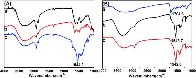 | ||
| Fig. 1 ATR-IR spectra of A: (a) Anodized TiO2 NTs, (b) TiO2 NTs-initiator modified, (c) TiO2 NTs-PMAA-Cd. B: (a) TiO2 NTs-PMAA-CdS, (b) TiO2 NTs-PMAA-Na-CdS, (c) TiO2 NTs- PMAA-Cd-CdS. | ||
3.2. FESEM images and elemental analysis
Fig. 2(A–F) represents the surface topography of TiO2 NTs, CdS-TiO2 NTs and CdS/CdSe-TiO2 NTs and their cross-section morphology obtained by FESEM (Fig. 2D–F). Fig. 2(A) shows the FESEM view of anodized TiO2 NTs, highly ordered alignment of nanotubes with well-defined tubular structures and smooth walls is clearly evident. The pore size ranges from 90 nm to 120 nm, and the average size is approximately 100 nm. Fig. 2(B) depicts that CdS nanoparticles are introduced onto TiO2 NTs, some precipitates on the surface make TiO2 NTs rather rougher than plain TiO2 NTs. After further loading with CdSe nanoparticles, as seen from Fig. 2 (C), CdSe/CdS QDs decorated TiO2 NTs have thicker tube walls than non-decorated ones due to the appearance of surface precipitates, and some nanoparticles have blocked the tube mouths, which could be used to confirm that CdSe/CdS QDs have been formed on the surfaces of TiO2 NTs.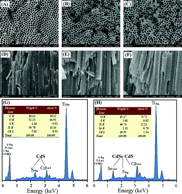 | ||
| Fig. 2 FESEM images the surfaces of (A) Anodized TiO2 NTs arrays; (B) CdS-TiO2 NTs; (C) CdSe/CdS-TiO2 NTs. Cross-section FESEM views of (D) plain TiO2 NTs; (E) CdS-TiO2 NTs; (F) CdSe/CdS-TiO2 NTs. Energy dispersive spectroscopy (EDS) spectra on cross-section: (G) CdS-TiO2 NTs and (H) CdSe/CdS-TiO2 NTs. | ||
Cross-section FESEM images were used to verify the QDs loading on the tube walls. Fig. 2(D) displays a cross-sectional FESEM image of the anodized TiO2 NTs, having apparent tubular morphology with smooth tube walls. The nanotube length is about 20 μm, which is the optimum length for nanotubes in dye sensitized solar cells for realizing the highest efficiency.45Fig. 2(E) is a FESEM image of TiO2 NTs after CdS loading, as can be seen clearly that well dispersed nanoparticles are decorated on both the inner and outer walls, which makes the nanotubes rougher than the plain TiO2 NTs. Fig. 2(F) is a cross-section FESEM image of CdS/CdSe-TiO2 NTs, which shows that high density nanoparticles have covered both the inner and outer walls of the TiO2 NTs. The direct contact between TiO2 and the semiconducting QDs is helpful for maximizing the charge separation efficiency in solar cell devices. After the introduction of secondary QDs, the nanotube walls showed enhanced roughness after CdSe QDs loading.
Energy dispersive spectroscopy (EDS) was employed to further confirm the successful CdS/CdSe QDs loading on TiO2 NTs. Fig. 2(G) shows the EDS analysis of a cross-section of the CdS-TiO2 NTs. It indicates the as-prepared sample contains Cd and S elements, and the Ti and O signals originated from the TiO2 and Ti substrate. EDS quantitative analysis of CdS-TiO2 NTs also gives a precisely 1:1 stoichiometric ratio of Cd to S (Cd, 0.92%; S, 0.92%), which can confirm the formation of the CdS compound. In Fig. 2(H), the Se signal additionally appears besides the S and Cd peaks after the preparation of CdSe QDs, which provides direct proof that CdSe and CdS QDs co-exist on TiO2 NTs. From the quantitative analysis of CdSe/CdS-TiO2 NTs, the atom ratio of Cd (2.54%) is larger than the total amount of S and Se (1.52%), which is probably due to the incomplete conversion of Cd ions to CdSe/CdS QDs.
3.3. Chemical composition analysis
Successful initiator modification, polymer grafting, and CdS/CdSe QDs loading on TiO2 NTs were verified by XPS. Fig. 3(A) shows the XPS survey spectra of TiO2 NTs (a), TiO2 NTs-initiator modified (b), TiO2 NTs-PMMA-Cd (c) and TiO2 NTs-PMMA-CdS (d). TiO2 NTs are mainly composed of Ti and O as well as a small amount of C resulting from adventitious hydrocarbon contamination. Successful anchoring of initiator-modified TiO2 NTs was confirmed by the presence of N signals not detected for the TiO2 NTs. After surface initiated polymerization on TiO2 NTs, polymer grafting was verified by high-resolution XPS spectral analysis in Fig. 3(C), which shows that the Cd 3d peaks appeared at binding energies of about 405.8 eV and 412.6 eV. After reaction with H2S gas, successful loading of CdS nanoparticles onto TiO2 NTs was primarily confirmed by the signals of the S (2p) peak at binding energies of 160.9 and 162.2 eV (Fig. 3(D)).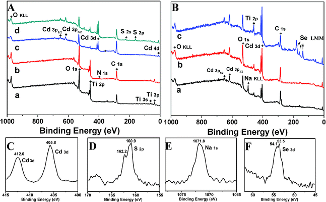 | ||
| Fig. 3 XPS survey spectra of A: (a) TiO2 NTs, (b) initiator modified TiO2 NTs, (c) TiO2 NTs-PMAA-Cd, (d) TiO2 NTs-PMAA-CdS. B: (a) TiO2 NTs-PMAA-CdS-Na, (b) TiO2 NTs-PMAA-CdS-Cd, (c) TiO2 NTs-PMAA-CdS-CdSe. (C): XPS survey spectra of Cd (3d) of TiO2 NTs-PMAA-Cd. (D): S (2p) of TiO2 NTs-PMAA-CdS. (E): Na (1s) of TiO2 NTs-PMAA-CdS-Na. (F): Se (3d) of TiO2 NTs-PMAA-CdS-CdSe. | ||
In order to reuse the polymer brushes for the secondary QDs loading, an ion exchange strategy was performed to immobilize Cd ions into polymer brushes. Fig. 3(B) displays the XPS survey spectra of TiO2 NTs-PMAA-CdS-Na, (b) TiO2 NTs-PMAA-CdS and (c) TiO2 NTs-PMAA-CdS-CdSe. TiO2 NTs-PMAA-CdS was dipped in NaOH solution (methanol as solvent) to exchange Na+ for the production of TiO2 NTs-PMAA-CdS-Na, as depicted in Fig. 3(E), the appearance of a Na (1s) signal at 1071.7 eV is the direct proof of the successful cation exchange. Also, the peaks of Na KLL in Fig. 3B(a) can be used to further confirm the Na+ exchange, and the clear Cd 3d peaks in Fig. 3B(b) prove the successful replacement of Na+ ions by Cd2+ cations. High-resolution XPS measurements were performed to analyze the Se species in CdSe quantum dots as shown in Fig. 3(F), where Se peaks appear at 53.5 and 54.1 eV (Se 3d).
3.4. Structure analysis
X-ray diffraction (XRD) experiments were used to determine the phase structure of these materials, all samples were annealed at 500 °C under N2 protection before measurement. Fig. 4(a) is an experimental XRD profile of TiO2 NTs that have been sintered at 450 °C under air, all the diffraction peaks corresponding to (101), (004), (200), (105), (211) and (204) can be indexed by the anatase phase of TiO2 (JCPDS file No. 78-2486) and metallic Ti substrate (JCPDS file No. 1-1197), respectively.43Fig. 4(b) is an experimental XRD profile of CdSe/CdS-TiO2 NTs. It can be easily concluded from the standard card (JCPDS file No. 19-191) that the diffraction peaks corresponding to the (111), (220), (311) planes of CdSe after being sintered to induce crystallization can be readily indexed as the cubic CdSe phase, which is consistent with a previous report.46Fig. 4(c) is an XRD profile of annealed CdS-TiO2 NTs, showing the diffraction peaks of (100), (002), (101), (102), (110), (103) and (112) we can easily conclude that the CdS nanoparticles actually have hexagonal structure (JCPDS file No. 1-783).47 Additionally, in Fig. 4(b), some peaks of CdS can also be seen, indicating the co-existence of CdS and CdSe QDs.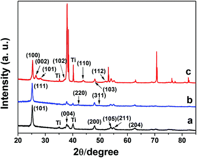 | ||
| Fig. 4 Experimental XRD profiles taken from (a) bare TiO2 NTs, (b) CdS/CdSe-TiO2 NTs and (c) CdS-TiO2 NTs. | ||
3.5. Photoelectric properties
In solar cell devices, when CdS and CdSe are used to sensitize TiO2 materials with a cascade structure, the conduction band and valence band of the three materials are in the following order: TiO2 < CdS < CdSe as shown in Fig. 5(A), which was very efficient in accelerating charge separation and exciton injection, thus a greatly expanded spectral response of TiO2 can be obtained.28 In order to confirm the spectral absorption of conventional anodized TiO2 NTs and CdS/CdSe QDs sensitized TiO2 NTs, UV-vis diffuse-reflectance spectra are shown in Fig. 5(B), the plain TiO2 NTs only have ultraviolet response. In order to further broaden the photoresponse of TiO2 to the visible light region, CdS QDs were incorporated into TiO2 NTs and thus the reflectance spectrum has been efficiently extended to approximately 550 nm, corresponding to the energy band gap of CdS (2.25 eV). For further broadening of the spectral absorption, CdSe QDs were fabricated onto TiO2 NTs, due to its narrow energy band gap of 1.7 eV, the reflectance spectrum is extended to 700 nm, towards even wider visible light absorption.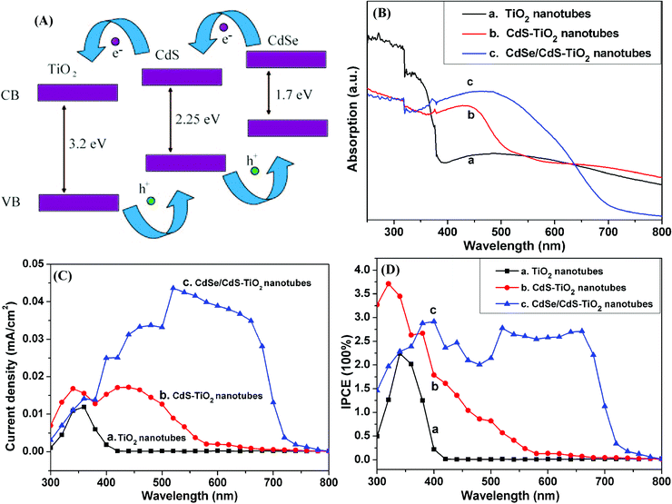 | ||
| Fig. 5 (A) The band edge structure for the efficient transport of the excited electrons and holes in CdS/CdSe co-sensitized TiO2 NTs. (B) UV-vis diffuse-reflectance spectra of (a) Anodized TiO2 NTs, (b) CdS-TiO2 NTs, (c) CdSe/CdS-TiO2 NTs. (C) The photocurrent dependence on the wavelength of illumination monochromatic light: (a) TiO2 NTs; (b) CdS-TiO2 NTs; (c) CdSe/CdS-TiO2 NTs. (D) Incident photon to current conversion efficiencies (IPCEs) measured as a function of wavelength for QDs-sensitized TiO2 NTs: (a) TiO2 NTs; (b) CdS-TiO2 NTs; (c) CdSe/CdS-TiO2 NTs. | ||
A comparison between the as-prepared TiO2 NTs and CdSe/CdS-TiO2 NTs was made using a two-electrode photoelectrochemical cell in 0.1 M Na2S solution. Fig. 5(C) provides typical photocurrent responses of TiO2 NTs before and after modification with CdS and CdSe/CdS QDs, the plain TiO2 NTs shows very low photocurrent density under visible irradiation (Fig. 5(C)a), corresponding to the bandgap of anatase TiO2 (3.2 eV) that only possess ultraviolet photoresponse.28 After the loading of CdS QDs, the photocurrent increased from 400 nm to 550 nm as shown in Fig. 5(C)b, which matches with the bandgap of CdS (2.25 eV) that can extend the spectral response of TiO2 to 550 nm. TiO2/CdS is the superior combination to harvest solar energy due to the higher conduction band edge of CdS with respect to that of TiO2, which has advantages to realize efficient electron transfer. For further expanding the photo absorption, CdSe QDs were prepared and showed enhanced photocurrent almost in the entire visible region (Fig. 5(C)c).
In general, the IPCE spectra of CdS-TiO2 and CdSe/CdS-TiO2 should be consistent with the corresponding UV-vis diffuse-reflectance spectra shown in Fig. 5(B). The incident photon to current conversion efficiency (IPCE) spectra are depicted in Fig. 5(D) and show a much wider light harvesting range after CdS/CdSe QDs loading on TiO2. IPCE values increase in the spectrum of 400 nm to 550 nm achieved by the CdS QDs sensitization, the energy band gap matching of CdS and TiO2 is the major driving force for the efficient charge transfer between CdS and TiO2. When CdSe QDs are prepared on CdS QDs sensitized TiO2 NTs, a higher IPCE is obtained in the short-wavelength region (<500 nm), where both CdS and CdSe QDs are photoactive so that the increase of IPCE mainly depends on the CdSe QDs. TiO2/CdS/CdSe architecture is the perfect combination for visible light harvesting and higher charge separation and transfer efficiencies. In the long-wavelength visible light region (>500 nm), where only CdSe materials can be photoexcited, the IPCE is greatly enhanced and extended into the visible region.
To better understand the roles of CdS and CdSe QDs, reproducible photocurrent and photovoltage responses to on-off light cycles were tested and shown in Fig. 6(A) and (B). As depicted in Fig. 6(A), the plain TiO2 NTs shows smaller photocurrent density than CdS-TiO2 NTs, and after the introduction of CdSe QDs the photocurrent is greatly enhanced. When the illuminated light was regularly switched on and off, a series of almost identical electric signals appeared and it was very stable after several cycling measurements. Furthermore, the photovoltage response in Fig. 6(B) is also regular under light on-off tests and shows reversible switching properties. The CdSe/CdS-TiO2 NTs electrode has the largest open circuit voltage (Voc) and a more negative potential than CdS-TiO2 NTs and TiO2 NTs, ensuring the biggest photoresponse upon light illumination. As an n-type semiconductor, TiO2, the electron was excited from the valance band to the conduction band under light illumination, and the open circuit potential of an n-type semiconductor is negative.48
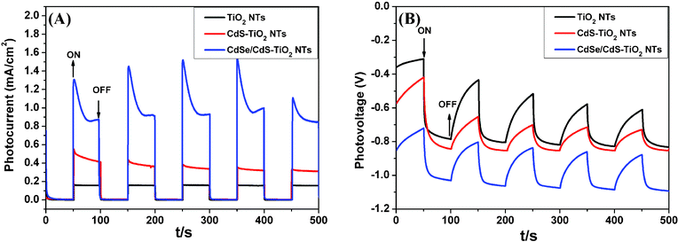 | ||
| Fig. 6 Photocurrent (A) and photovoltage (B) responses of TiO2 NTs, CdS-TiO2 NTs and CdSe/CdS-TiO2 NTs. | ||
4. Conclusions
In summary, surface-initiated polymerization has been employed to graft polymer brushes onto the surfaces of TiO2 nanotubes for CdS/CdSe QDs loading with the aim of being able to tune the response of TiO2 to the visible region. These polymer brushes provide a nano-confined environment as the template for CdS and CdSe QDs formation with uniform dispersion on TiO2 surfaces. The spectral absorption of these composite materials has been extended to the visible region and the composite materials show strong reversible photoelectric responses.Acknowledgements
The authors gratefully acknowledge the support of NSFC (20973188, 21125316) and the “Hundred Talents Program” of Chinese Academy of Sciences.References
- R. Li, D. Liu, D. Zhou, Y. Shi, Y. Wang and P. Wang, Energy Environ. Sci., 2010, 3, 1765 CAS
.
- F. Gao, Y. Wang, D. Shi, J. Zhang, M. Wang, X. Jing, R. Humphry-Baker, P. Wang, S. M. Zakeeruddin and M. Grätzel, J. Am. Chem. Soc., 2008, 130, 10720 CrossRef CAS
- S. Lim and S. Rhee, RSC Adv., 2011, 1, 518 RSC
- H. Lee, M. Wang, P. Chen, D. R. Gamelin, S. M. Zakeeruddin, M. Grätzel and M. K. Nazeeruddin, Nano Lett., 2009, 9, 4221 CrossRef CAS
- G. K. Mor, S. Kim, M. Paulose, O. K. Varghese, K. Shankar, J. Basham and C. A. Grimes, Nano Lett., 2009, 9, 4250 CrossRef CAS
- Q. Tai, X. Zhao and F. Yan, J. Mater. Chem., 2010, 20, 7366 RSC
- D. Wang, Q. Ye, B. Yu and F. Zhou, J. Mater. Chem., 2010, 20, 6910 RSC
- P. Roy, D. Kim, K. Lee, E. Spiecker and P. Schmuki, Nanoscale, 2010, 2, 45 RSC
- K. Shankar, J. Bandara, M. Paulose, H. Wietasch, O. K. Varghese, G. K. Mor, T. J. LaTempa, M. Thelakkat and C. A. Grimes, Nano Lett., 2008, 8, 1654 CrossRef CAS
- I. Robel, V. Subramanian, M. Kuno and P. V. Kamat, J. Am. Chem. Soc., 2006, 128, 2385 CrossRef CAS
- P. Roy, S. Berger and P. Schmuki, Angew. Chem., Int. Ed., 2011, 50, 2904 CrossRef CAS
- J. Y. Li, C. Y. Chen, J. G. Chen, C. J. Tan, K. M. Lee, S. J. Wu, Y. L. Tung, H. H. Tsai, K. C. Ho and C. G. Wu, J. Mater. Chem., 2010, 20, 7158 RSC
- Y. Shengyuan, A. S. Nair, R. Jose and S. Ramakrishna, Energy Environ. Sci., 2010, 3, 2010 Search PubMed
- S. Bingham and W. A. Daoud, J. Mater. Chem., 2011, 21, 2041 RSC
- M. K. Nazeeruddin, F. D. Angelis, S. Fantacci, A. Selloni, G. Viscardi, P. Liska, S. Ito, B. Takeru and M. Grätzel, J. Am. Chem. Soc., 2005, 127, 16835 CrossRef CAS
- A. Mishra, M. K. R. Fischer and P. Bäuerle, Angew. Chem., Int. Ed., 2009, 48, 2474 CrossRef CAS
- S. Q. Fan, D. Kim, J. J. Kim, D. W. Jung, S. O. Kang and J. Ko, Electrochem. Commun., 2009, 11, 1337 CrossRef CAS
- A. Kongkanand, K. Tvrdy, K. Takechi, M. Kuno and P. V. Kamat, J. Am. Chem. Soc., 2008, 130, 4007 CrossRef CAS
- Y. L. Lee, B. M. Huang and H. T. Chien, Chem. Mater., 2008, 20, 6903 CrossRef CAS
- W. T. Sun, Y. Yu, H. Y. Pan, X. F. Gao, Q. Chen and L. M. Peng, J. Am. Chem. Soc., 2008, 130, 1124 CrossRef CAS
- D. R. Baker and P. V. Kamat, Adv. Funct. Mater., 2009, 19, 805 CrossRef CAS
- S. Chen, M. Paulose, C. Ruan, G. K. Mor, O. K. Varghese, D. Kouzoudis and C. A. Grimes, J. Photochem. Photobiol., A, 2006, 177, 177 CrossRef CAS
- X. F. Gao, W. T. Sun, Z. D. Hu, G. Ai, Y. L. Zhang, S. Feng, F. Li and L. M. Peng, J. Phys. Chem. C, 2009, 113, 20481 CAS
- K. Shin, S. i. S, S. H. Im and J. H. Park, Chem. Commun., 2010, 46, 2385 RSC
- C. Ratanatawanate, C. Xiong and K. J. B. Jr, ACS Nano, 2008, 2, 1682 CrossRef CAS
- X. F. Gao, H. B. Li, W. T. Sun, Q. Chen, F. Q. Tang and L. M. Peng, J. Phys. Chem. C, 2009, 113, 7531 CAS
- W. Zhu, X. Liu, H. Liu, D. Tong, J. Yang and J. Peng, J. Am. Chem. Soc., 2010, 132, 12619 CrossRef CAS
- Y. L. Lee and Y. S. Lo, Adv. Funct. Mater., 2009, 19, 604 CrossRef
- O. Azzaroni, S. E. Moya, A. A. Brown, Z. Zheng, E. Donath and W. T. S. Huck, Adv. Funct. Mater., 2006, 16, 1037 CrossRef CAS
- X. Wang, H. Hu, Y. Shen, X. Zhou and Z. Zheng, Adv. Mater., 2011, 23, 3090 CrossRef CAS
- Z. Liu, H. Hu, B. Yu, M. Chen, Z. Zheng and F. Zhou, Electrochem. Commun., 2009, 11, 492 CrossRef CAS
- X. Liu, H. Chang, Y. Li, W. T. S. Huck and Z. Zheng, ACS Appl. Mater. Interfaces, 2010, 2, 529 CAS
- R. Barbey, L. Lavanant, D. Paripovic, N. Schüwer, C. Sugnaux, S. Tugulu and H. Klok, Chem. Rev., 2009, 109, 5437 CrossRef CAS
- A. Calvo, M. C. Fuertes, B. Yameen, F. J. Williams, O. Azzaroni and G. J. A. A. Soler-Illia, Langmuir, 2010, 26, 5559 CrossRef CAS
- L. Ionov, S. Sapra, A. Synytska, A. L. Rogach, M. Stamm and S. Diez, Adv. Mater., 2006, 18, 1453 CrossRef CAS
- Q. Ye, F. Zhou and W. Liu, Chem. Soc. Rev., 2011, 40, 4244 RSC
- Q. Ye, X. Wang, S. Li and F. Zhou, Macromolecules, 2010, 43, 5554 CrossRef CAS
- O. Azzaroni, Z. Zheng, Z. Yang and W. T. S. Huck, Langmuir, 2006, 22, 6730 CrossRef CAS
- O. Azzaroni, A. A. Brown, N. Cheng, A. Wei, A. M. Jonas and W. T. S. Huck, J. Mater. Chem., 2007, 17, 3433 RSC
- Q. Ye, X. Wang, H. Hu, D. Wang, S. Li and F. Zhou, J. Phys. Chem. C, 2009, 113, 7677 CAS
- X. Fan, L. Lin, J. L. Dalsin and P. B. Messersmith, J. Am. Chem. Soc., 2005, 127, 15843 CrossRef CAS
- T. Cui, J. Zhang, J. Wang, F. Cui, W. Chen, F. Xu, Z. Wang, K. Zhang and B. Yang, Adv. Funct. Mater., 2005, 15, 481 CrossRef CAS
- D. Wang, B. Yu, C. Wang, F. Zhou and W. Liu, Adv. Mater., 2009, 21, 1964 CrossRef CAS
- D. Wang, Y. Liu, B. Yu, F. Zhou and W. Liu, Chem. Mater., 2009, 21, 1198 CrossRef CAS
- J. Yan and F. Zhou, J. Mater. Chem., 2011, 21, 9406 RSC
- J. H. Bang and P. V. Kamat, Adv. Funct. Mater., 2010, 20, 1970 CrossRef CAS
- J. Cao, J. Sun, H. Li, J. Hong and M. Wang, J. Mater. Chem., 2004, 14, 1203 RSC
- C. J. Brabec, A. Cravino, D. Meissner, N. S. Sariciftci, T. Fromherz, M. T. Rispens, L. Sanchez and J. C. Hummelen, Adv. Funct. Mater., 2001, 11, 374 CrossRef CAS
| This journal is © The Royal Society of Chemistry 2012 |