Efficient small molecule organic semiconductor containing bis-dimethylfluorenyl amino benzo[b]thiophene for high open circuit voltage in high efficiency solution processed organic solar cell†
Jooyoung
Kim
a,
Haye Min
Ko
a,
Nara
Cho
a,
Sanghyun
Paek
a,
Jae Kwan
Lee
*b and
Jaejung
Ko
*a
aDepartment of New Material Chemistry, Korea University, Chungnam 330-700, Republic of Korea. E-mail: jko@korea.ac.kr; Fax: +82-41-860-5396; Tel: +82-41-860-1337
bDepartment of Chemistry Education, Chosun University, Gwangju 501-759, Republic of Korea. E-mail: chemedujk@chosun.ac.kr; Fax: +82-62-232-8122; Tel: +82-62-230-7368
First published on 11th January 2012
Abstract
A new small molecule organic semiconductor, bisDMFABT-Th-MMN, containing a benzothiophene donor and methylene-malononitrile acceptor, exhibited high power conversion efficiency of 4.01% with a high open circuit voltage of 0.95 V in solution processed small molecule organic solar cells.
Solution processed organic solar cells (OSCs) fabricated by means of versatile printing techniques such as doctor blade, inkjet, and roll-to-roll can provide many attractive features, including low cost, light weight, and solution processability. Over the last few years, enormous effort has been focused on improving device performances towards power conversion efficiency (PCE) of 10% though developments of photoactive materials such as π-conjugated (semiconducting) polymers and fullerene derivatives, or functional layers such as buffering, charge transporting, and optical spacing.1 Recently, great achievements in obtaining PCEs of above 8% has rendered OSCs strong candidates for next generation solar cells, threatening the position of inorganic thin film solar cells as well as dye-sensitized solar cells (DSSCs).2 Most of these high efficiencies have been reported in OSCs fabricated with bulk heterojunction (BHJ) materials comprised of low-bandgap semiconducting polymers and [6,6]-phenyl-C61 (or 71)-butyric acid methyl ester (C61(or 71)-PCBM).3 Nevertheless, small molecule photosensitizers seem to be of greater interest than these polymers from the viewpoint of mass production for commercial application, due to the low reproducibility of characteristics such as average molecular weight (Mw) and polydispersity index (PDI) as well as the difficulty in purification exhibited by these polymers. Motivated by this, considerable research effort has been focused on developing efficient small molecule materials for improved device performance, with the short-term goal being a PCE comparable to polymer-based solar cells (PSCs).4 Indeed, recent breakthroughs in realizing PCEs of above 6% have placed solution processed small molecule organic solar cells (SMOSCs) squarely in competition with PSCs.5
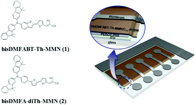
Very recently, we have also reported an efficient organic semiconductor for solution processed SMOSCs, which was motivated by organic dyes in DSSCs and push–pull chromophores in nonlinear optics (NLO) due to a strong structural similarity with small molecule organic semiconductors reported in BHJ solar cells, showing a PCE of 3.6%.6 This successful approach led us to attempt to develop a higher efficiency small molecule organic semiconductor, considering the correlation of photophysical and photochemical properties with the structures of DSSC organic dyes or NLO chromophores. Herein, we report the synthesis and photovoltaic characteristics of a new small molecule organic semiconductor, 2-((5′-(4-(bis(9,9-dimethyl-9H-fluoren-2-yl)amino)benzo[b]thiophene)-2,2′-thiophen-5-yl)methylene)malononitrile (bisDMFABT-Th-MMN, 1), which showed a PCE of 4.01% with a high open circuit voltage of 0.95 V. This was compared with 2-((5′-(4-(bis(9,9-dimethyl-9H-fluoren-2-yl)amino)phenyl)-2,2′-bithiophen-5-yl)methylene)malononitrile (bisDMFA-diTh-MMN, 2) reported previously. (Scheme 1)
 | ||
| Scheme 1 Molecular structure of bisDMFABT-Th-MMN and the device architecture of the solution processed small molecule organic solar cell. | ||
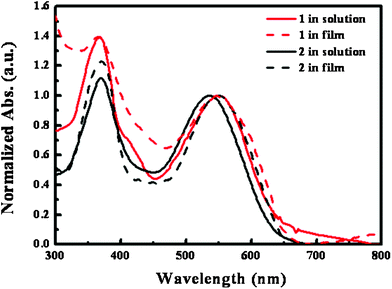
1 was readily synthesized by a Knoevenagel condensation reaction using 5-(6-(bis(9,9-dimethyl-9H-fluoren-2-yl)amino)benzo[b]thiophen-2-yl)thiophene-2-carbaldehyde, which was prepared according to a reported procedure,7 and methylene-malononitrile (MMN) as an effective electron withdrawing group. Fig. 1 shows the UV-vis absorption spectra of 1 and 2 in chlorobenzene solution and thin films. The corresponding optical properties are summarized in Table 1.
 | ||
| Fig. 1 UV-vis absorption spectra of 1 (black) and 2 (red) in chlorobenzene solution (solid line) and thin films (dashed line). | ||
| Material | λ abs a/nm (ε/M−1cm−1) | E onset, ox(V)/HOMO (eV)b | LUMO (eV) | E 0-0 (eV)c | E onset (eV) |
|---|---|---|---|---|---|
| a Absorption spectra were measured in chlorobenzene solution. b Redox potentials of the materials were measured in CH2Cl2 with 0.1 M (n-C4H9)4NPF6 with a scan rate of 100 mV s−1 (vs. Fc/Fc+). c E 0-0 was calculated from the absorption thresholds from absorption spectra of films spin-cast on quartz substrate. | |||||
| 1 | 550 (40![[thin space (1/6-em)]](https://www.rsc.org/images/entities/char_2009.gif) 445) 445) |
0.238/−5.038 | −3.456 | 1.98 | 1.95 |
| 2 | 536 (32![[thin space (1/6-em)]](https://www.rsc.org/images/entities/char_2009.gif) 174) 174) |
0.116/−4.916 | −2.946 | 1.97 | 1.94 |
As shown in Fig. 1a, the absorption spectrum of 1 and 2 in solution shows intramolecular charge transfer (ICT) in the region 400–700 nm and molar absorption coefficients of 40![[thin space (1/6-em)]](https://www.rsc.org/images/entities/char_2009.gif) 445 M−1cm−1 at 550 nm, and 32
445 M−1cm−1 at 550 nm, and 32![[thin space (1/6-em)]](https://www.rsc.org/images/entities/char_2009.gif) 174 M−1cm−1 at 536 nm, respectively. The organic semiconductor having the benzothiophene moiety exhibits an ∼14 nm red-shifted absorption spectrum and ∼26% enhanced molar extinction coefficient due to its longer conjugation length compared with 2. However, in the solid-state thin film, the absorption spectrum of 1 did not show a red-shift but a broadened ICT band compared to that in solution, resulting in similar absorption characteristics to 2. This result suggests that 1 might be unfavorable for intermolecular π–π packing due to the rather small molecule size, despite the enhanced molecular planarity compared to 2. Also, the energy levels of the highest occupied molecular orbital (HOMO) and the lowest unoccupied molecular orbital (LUMO) of these materials were determined from cyclic voltammetry (CV) analysis and the corresponding electrochemical properties are also summarized in Table 1. The CV of these materials in solid-state thin film could not be measured due to the stripping of the film on the electrode. Therefore, we determined the optical bandgap from calculation of the absorption thresholds from absorption spectra of 1 and 2 in chlorobenzene. The HOMO levels of 1 and 2 determined in solution by CV are calculated as 5.038 eV and 4.916 eV, respectively. From these results, we can roughly estimate that the Voc of devices fabricated using these materials/PCBM BHJ active layer may be greater than 0.7 V.8 However, it is of interest to note that a high Voc of 0.95 V for the device fabricated using 1 was found in this experiment.
174 M−1cm−1 at 536 nm, respectively. The organic semiconductor having the benzothiophene moiety exhibits an ∼14 nm red-shifted absorption spectrum and ∼26% enhanced molar extinction coefficient due to its longer conjugation length compared with 2. However, in the solid-state thin film, the absorption spectrum of 1 did not show a red-shift but a broadened ICT band compared to that in solution, resulting in similar absorption characteristics to 2. This result suggests that 1 might be unfavorable for intermolecular π–π packing due to the rather small molecule size, despite the enhanced molecular planarity compared to 2. Also, the energy levels of the highest occupied molecular orbital (HOMO) and the lowest unoccupied molecular orbital (LUMO) of these materials were determined from cyclic voltammetry (CV) analysis and the corresponding electrochemical properties are also summarized in Table 1. The CV of these materials in solid-state thin film could not be measured due to the stripping of the film on the electrode. Therefore, we determined the optical bandgap from calculation of the absorption thresholds from absorption spectra of 1 and 2 in chlorobenzene. The HOMO levels of 1 and 2 determined in solution by CV are calculated as 5.038 eV and 4.916 eV, respectively. From these results, we can roughly estimate that the Voc of devices fabricated using these materials/PCBM BHJ active layer may be greater than 0.7 V.8 However, it is of interest to note that a high Voc of 0.95 V for the device fabricated using 1 was found in this experiment.
The performances of 1 and 2 were investigated through the application of photovoltaic devices fabricated with these materials/C71-PCBM BHJ films. In the course of studying the characteristics of over 400 solar cells, the most efficient photovoltaic cells fabricated using 2/PC71BM were optimized at ratio of 1![[thin space (1/6-em)]](https://www.rsc.org/images/entities/char_2009.gif) :
:![[thin space (1/6-em)]](https://www.rsc.org/images/entities/char_2009.gif) 2, but 1/PC71BM was optimized at ratio of approximately 1
2, but 1/PC71BM was optimized at ratio of approximately 1![[thin space (1/6-em)]](https://www.rsc.org/images/entities/char_2009.gif) :
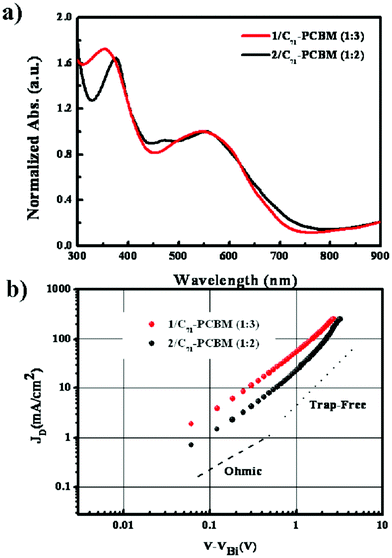
:![[thin space (1/6-em)]](https://www.rsc.org/images/entities/char_2009.gif) 3. These BHJ films were cast on top of a PEDOT:PSS (Heraeus, AI 4083) layer. The optimum thicknesses of both 1/C71-PCBM and 2/C71-PCBM BHJ films obtained under these conditions were around 70 nm. Fig. 2a shows the UV-visible absorption spectra of these BHJ films and the extracted hole mobility from the space-charge limitation of current (SCLC) J–V characteristics of these BHJ films obtained in the dark for hole-only ITO/PEDOT:PSS/1 (or 2):C71-PCBM/Au devices.
3. These BHJ films were cast on top of a PEDOT:PSS (Heraeus, AI 4083) layer. The optimum thicknesses of both 1/C71-PCBM and 2/C71-PCBM BHJ films obtained under these conditions were around 70 nm. Fig. 2a shows the UV-visible absorption spectra of these BHJ films and the extracted hole mobility from the space-charge limitation of current (SCLC) J–V characteristics of these BHJ films obtained in the dark for hole-only ITO/PEDOT:PSS/1 (or 2):C71-PCBM/Au devices.
 | ||
Fig. 2 UV-vis absorption spectra and space charge limitation of current J–V characteristics of 1/C71-PCBM (1![[thin space (1/6-em)]](https://www.rsc.org/images/entities/char_2009.gif) : :![[thin space (1/6-em)]](https://www.rsc.org/images/entities/char_2009.gif) 3) (red) and 2/C71-PCBM (1 3) (red) and 2/C71-PCBM (1![[thin space (1/6-em)]](https://www.rsc.org/images/entities/char_2009.gif) : :![[thin space (1/6-em)]](https://www.rsc.org/images/entities/char_2009.gif) 2) (black) BHJ films. 2) (black) BHJ films. | ||
As shown in Fig. 2b, the hole mobility of 1 and 2 evaluated from SCLC analysis of these BHJ films using the Mott–Gurney Law (ε= 3ε0)9 were 3.59 × 10⁻⁵ cm2 V−1 s−1 and 2.26 × 10⁻⁵ cm2 V−1 s−1, respectively. 1, having the benzothiophene moiety, exhibited about 1.6 times higher mobility than 2. From these results, we note that the intermolecular π–π interaction could occur efficiently in 1 due to its structural planarity, showing more favorable hole-transporting features than 2 despite its rather poor packing structure as shown in Fig. 1.
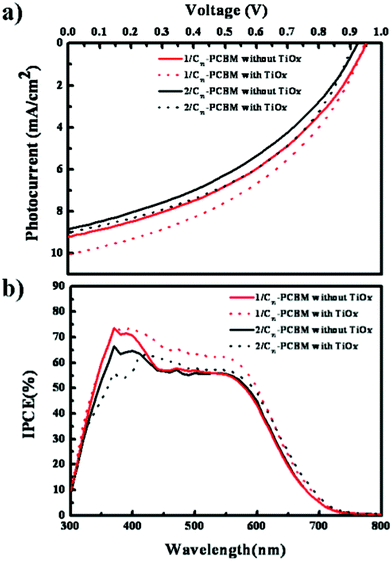
Fig. 3a shows the current (J)–voltage (V) curves under AM 1.5 conditions (100 mW cm−2) and the incident photon-to-current conversion efficiency (IPCE) of 1/C71-PCBM and 2/PC71BM BHJ solar cells with/without TiOx functional layer,10 which can play the effective roles of optical spacer and buffer layer, under the optimized conditions and the corresponding values are summarized in Table 2. As shown in Fig. 3 and Table 2, the best PCE of 4.01% (±0.12) in devices fabricated using 1/C71-PCBM film with TiOx layer was observed with short-circuit current (Jsc) = 10.05 mA cm−2, fill factor (FF) = 0.42, and open-circuit voltage (Voc) = 0.95 V, which is ∼12% higher efficiency than that without a TiOx layer. Also 1, having a benzothiophene unit, exhibited better photovoltaic performances with increased Jsc and Voc compared with 2, resulting in ∼12% higher efficiency of SMOSCs. This may be caused by the higher hole-mobility of 2.
 | ||
Fig. 3 UV-vis absorption spectra and space charge limitation of current J–V characteristics of the 1/C71-PCBM (1![[thin space (1/6-em)]](https://www.rsc.org/images/entities/char_2009.gif) : :![[thin space (1/6-em)]](https://www.rsc.org/images/entities/char_2009.gif) 3) (red) and 2/C71-PCBM (1 3) (red) and 2/C71-PCBM (1![[thin space (1/6-em)]](https://www.rsc.org/images/entities/char_2009.gif) : :![[thin space (1/6-em)]](https://www.rsc.org/images/entities/char_2009.gif) 2) (black) BHJ films. 2) (black) BHJ films. | ||
| Donor | Functional layer | J sc (mA cm−2) | V oc (V) | FF (%) | η (%) |
|---|---|---|---|---|---|
a The optimum devices were fabricated both 1/C71-PCBM (1![[thin space (1/6-em)]](https://www.rsc.org/images/entities/char_2009.gif) : :![[thin space (1/6-em)]](https://www.rsc.org/images/entities/char_2009.gif) 3) and 2/C71-PCBM (1 3) and 2/C71-PCBM (1![[thin space (1/6-em)]](https://www.rsc.org/images/entities/char_2009.gif) : :![[thin space (1/6-em)]](https://www.rsc.org/images/entities/char_2009.gif) 2) with ∼70 nm thickness. The performances are determined under simulated 100 mW cm−2 AM 1.5G illumination. The light intensity using calibrated standard silicon solar cells with a proactive window was made from KG5 filter glass traced to the National Renewable Energy Laboratory (NREL). The masked active area of device is 4 mm2.
b Thermally post-annealed at 100 °C. 2) with ∼70 nm thickness. The performances are determined under simulated 100 mW cm−2 AM 1.5G illumination. The light intensity using calibrated standard silicon solar cells with a proactive window was made from KG5 filter glass traced to the National Renewable Energy Laboratory (NREL). The masked active area of device is 4 mm2.
b Thermally post-annealed at 100 °C.
|
|||||
| 1 | none | 9.21 | 0.95 | 41 | 3.57 |
| 1 | TiOx | 10.05 | 0.95 | 42 | 4.01 |
| 2 | none | 8.85b | 0.92b | 39b | 3.23b |
| 2 | TiOx | 9.00b | 0.91b | 44b | 3.58b |
The IPCE spectra as shown in Fig. 3b exhibited close correlation with their photocurrents in J–V curves. The 1/C71-PCBM BHJ film exhibited superior IPCE in its full absorption range compared with that of 2. Moreover, the devices with these BHJ films presented significantly enhanced IPCEs in the 400–700 nm wavelength regions after insertion of the TiOx optical spacer, affecting the increase in photocurrent.
The morphologies of these BHJ films investigated with atomic force microscopy (AFM) exhibited a good phase-separated bicontinuous network both 1/C71-PCBM and 2/C71-PCBM, resulting in the good photocurrents of SMOSCs. Also, the MMN acceptor unit has often given the high photovoltage in OSC,11 resulting in the Voc above 0.9 V in both 1 and 2.
Conclusions
We have demonstrated the synthesis and photovoltaic characteristics of a new small molecule organic semiconductor, 1, having a benzothiophene donor and methylene–malononitrile acceptor, which exhibited a high PCE of 4% with high open circuit voltage of 0.95 V in SMOSCs. The newly synthesized push–pull organic semiconductor, 1, comprised of bis(9,9-dimethyl-9H-fluoren-2-yl)amino)benzo[b]-thiophene donor and methylene–malononitrile acceptor showed moderate hole mobility despite the rather small molecule size, and the strong electron-withdrawing group of MMN can induce high Voc in solution processed SMOSCs. The results obtained from the molecular engineering approaches shown in this study can give an important guide for developing new materials in solution processed small molecule BHJ solar cells.Acknowledgements
The research was supported by the WCU (the Ministry of Education, Science and Technology) program (Grant No. R31-2011-000-10035-0) and MEST for the Center for Next Generation Dye-sensitized Solar Cells (No. 2011-0001055).References
- (a) D. Demeter, T. Rousseau, P. Leriche, T. Cauchy, R. Po and J. Roncali, Adv. Funct. Mater., 2011, 21, 4379 CrossRef CAS; (b) B. Walker, C. Kim and T.-Q. Nguyen, Chem. Mater., 2011, 23, 470 CrossRef CAS.
- M. A. Green, K. Emery, Y. Hishikawa, W. Warta and E. D. Dunlop, Prog. Photovoltaics, 2011, 19, 565 Search PubMed.
- (a) S. C. Price, A. C. Stuart, L. Yang, H. Zhou and W. You, J. Am. Chem. Soc., 2011, 133, 4625 CrossRef CAS; (b) H. Zhou, L. Yang, A. C. Stuart, S. C. Price, S. Liu and W. You, Angew. Chem., Int. Ed., 2011, 50, 2995 CrossRef CAS.
- (a) S. Roquet, A. Cravino, P. Leriche, O. Alévêque, P. Frère and J. Roncali, J. Am. Chem. Soc., 2006, 128, 3459 CrossRef CAS; (b) A. Cravino, P. Leriche, O. Aleveque, S. Roquet and J. Roncali, Adv. Mater., 2006, 18, 3033 CrossRef CAS; (c) A. B. Tamayo, X. D. Dang, B. Walker, J. Seo, T. Kent and T. Q. Nguyen, Appl. Phys. Lett., 2009, 94, 103301 CrossRef; (d) C. Q. Ma, M. Fonrodona, M. C. Schikora, M. M. Wienk, R. A. J. Janssen and P. Bauele, Adv. Funct. Mater., 2008, 18, 3323 CrossRef CAS; (e) Z. E. Ooi, T. L. Tam, R. Y. C. Shin, Z. K. Chen, T. Kietzke, A. Sellinger, M. Baumgarten, K. Mullen and J. C. deMello, J. Mater. Chem., 2008, 18, 4619 RSC.
- Y. Sun, G. C. Welch, W. L. Leong, C. J. Takacs, G. C. Bazan and A. J. Heeger, Nat. Mater., 2012, 11, 44 CrossRef CAS.
- (a) H. M. Ko, H. Choi, S. Paek, K. Kim, K. Song, J. K. Lee and J. Ko, J. Mater. Chem., 2011, 21, 7248 RSC; (b) J. K. Lee, W. L. Ma, C. J. Brabec, J. Yuen, J. S. Moo, J. Y. Kim, K. Lee, G. C. Bazan and A. J. Heeger, J. Am. Chem. Soc., 2008, 130, 3619 CrossRef CAS.
- H. Choi, J. K. Lee, K. Song, S. O. Kang and J. Ko, Tetrahedron, 2007, 63, 3115 CrossRef CAS.
- M. C. Scharber, D. Mühlbacher, M. Koppe, P. Denk, C. Waldauf, A. J. Heeger and C. J. Brabec, Adv. Mater., 2006, 18, 789 CrossRef CAS.
- V. D. Mihailetchi, H. Xie, B. Boer, L. J. A. Koster and P. W. M. Blom, Adv. Funct. Mater., 2006, 16, 699 CrossRef CAS.
- K. Lee, J. Y. Kim, S. H. Park, S. H. Kim, S. Cho and A. J. Heeger, Adv. Mater., 2007, 19, 2445 CrossRef CAS.
- J. Roncali, Acc. Chem. Res., 2009, 42, 1719 CrossRef CAS.
Footnote |
| † Electronic supplementary information (ESI) available. See DOI: 10.1039/c2ra01271e |
| This journal is © The Royal Society of Chemistry 2012 |
