Decoupling of CVD graphene by controlled oxidation of recrystallized Cu†
Ang-Yu
Lu
ab,
Sung-Yen
Wei
b,
Chih-Yu
Wu
b,
Yenny
Hernandez
c,
Tzu-Yin
Chen
a,
Te-Huan
Liu
a,
Chun-Wei
Pao
a,
Fu-Rong
Chen
b,
Lain-Jong
Li
*a and
Zhen-Yu
Juang
*ab
aResearch Center for Applied Sciences, Academia Sinica, Taipei, 11529, Taiwan. E-mail: lanceli@gate.sinica.edu.tw; Tel: +886 3 5712121 ext. 59484
bDepartment of Engineering and System Science, National Tsing Hua University, Hsinchu, 30013, Taiwan. E-mail: juang@ess.nthu.edu.tw; Fax: +886 3 5720724; Tel: +886 3 5715131 ext. 35804
cMax Planck Institute for Polymer Research, Ackermannweg 10, 55128, Mainz, Germany. E-mail: hernande@mpip-mainz.mpg.de; Fax: +49 0 6131 379 ext. 100; Tel: +49 0 6131 379 203
First published on 11th January 2012
Abstract
Large-area graphene grown by chemical vapour deposition (CVD) is promising for applications; however, the interaction between graphene and the substrate is still not well understood. In this report, we use a combination of two non-destructive characterization techniques, i.e., electron backscatter diffraction (EBSD) and Raman mapping to locally probe the interface between graphene and copper lattices without removing graphene. We conclude that the crystal structure of the Cu grains under graphene layers is governed by two competing processes: (1) graphene induced Cu surface reconstruction favoring the formation of Cu(100) orientation, and (2) recrystallization from bulk Cu favoring Cu(111) formation. The underlying Cu grains, regardless of reconstruction or recrystallization, induce a large hydrostatic compression to the graphene lattice. Interestingly, the strong interaction could be decoupled by allowing the intercalation of a thin cuprous oxide interfacial-layer. The Cu2O layer is mechanically and chemically weak; hence, graphene films can be detached and transferred to arbitrary substrates and the Cu substrates could be re-used for graphene growth.
Introduction
The unique electrical, physical and optical properties of graphene are promising for a variety applications in electronics.1 Tremendous efforts are being undertaken to develop methods to produce large-area, high quality graphene using chemical or electrochemical methods.2–4 Among various catalytic metal substrates for graphene growth using chemical vapour deposition (CVD),5–15 nickel (Ni) and copper (Cu) are so far the most promising metals for the production of large-area self-terminated films.14–18 Transparent conductive electrodes, high contrast transmission electron microscopy (TEM) grids,19 gas and biosensors,20 and nanoelectromechanical systems using CVD-grown graphene have been intensively studied and are promising for future applications.21As recently discussed by Chhowalla and co-workers, Cu represents the ideal catalyst for graphene growth due to its low affinity to carbon, where the graphene detachment and transfer processes are relatively easier than the graphene grown on Ni surfaces or epitaxially formed on silicon carbide surfaces.17 Although a few reports have suggested that the graphene growth may occur at certain crystallographic directions, Cu(100) and Cu(111),17 a detailed study has yet to be conducted. By using electron-backscattered diffraction (EBSD) mapping we can reveal the local lattice orientation of Cu substrates without removing the CVD-grown graphene films. Confocal Raman mapping is also applied to probe the graphene structure. Therefore, the spatially-resolved correlation between as-grown graphene and the underlying Cu structure can be realized.
Our results show that the surface of the commonly used Cu foil at high temperature change with the cooling rate after graphene growth and its structure is also affected by the presence of graphene. Surprisingly, the Cu grains oxidize at ambient conditions, with the oxidation rate depending on the interaction of the graphene layers with the underlying Cu.22 By using Raman mapping, we have realized that the strong interaction between graphene and Cu can be decoupled by introducing a layer of Cu2O in between graphene and Cu. The Cu2O is mechanically weak; hence, graphene films can be detached and transferred to arbitrary substrates and the Cu substrates can be reused for graphene growth.
Experimental section
CVD process: Centimetre-scaled graphene films were synthesized via a hot-wall furnace consisting of a 25 mm (inner diameter) quartz tube using Cu foil (25 μm in thickness, purity of 99.8%) as catalytic substrates as described by Li et al.16 The Cu foil typically has a native oxide layer on the surface, which must be removed for successful growth of graphene on Cu. Hence, after the Cu foil was loaded into the furnace, it was heated to the process temperature 1000 °C under a H2 atmosphere with 400 sccm flow at 500 Torr followed thermal annealing at the same temperature for 50 min. The growth of single-layer graphene (SLG) was then started with a CH4/H2 gas mixture (60 and 15 sccm, respectively) for 20 min at 750 mTorr. Subsequently the furnace was cooled to room temperature at fast (∼280 °C min−1) or slow (1.7 °C min−1) cooling rate. Note that the fast cooling procedure was conducted by opening and shutting-down the furnace immediately after growth, resulting in a non-linear temperature profile. Thus the cooling rate was estimated from 1000 °C to 900 °C, where the Cu crystallization is mostly governed by the initial cooling stage. The gas condition was maintained from the beginning of the growth stage to the end of the cooling stage. The gas flow rates were controlled by mass flow controllers (MFC, Brooks Instrument). The pressure was precisely monitored and controlled by Baratron® capacitance manometers (MKS Instrument) and a pressure controller (APC, MKS Instrument). If high purity Cu foils (99.999%) are used to grow graphene at 1000 °C, only defective carbon films are obtained on the polycrystalline Cu surface. A higher process temperature around 1030 °C is necessary for obtaining high quality graphene, indicating that the m.p. of the high purity Cu is significantly higher than the Cu foil with 99.8% purity.Oxidation process: After CVD growth, we took the Raman spectra from as-grown (non-oxide) graphene/Cu sample immediately. Subsequently, an additional ex-situ step of a few days ambient oxidation of Cu in air with considerable humidity level was performed. CVD-grown graphene is polycrystalline in nature, therefore, air present oxygen can penetrate at the grain boundaries resulting in a thin Cu oxide layer at the graphene/Cu interface. The thickness of Cu2O could be controlled by two parameters, i.e., temperature and humidity. In the case we mentioned, the temperature and humidity were kept at room-temperature and ∼50% respectively, and result in a thickness of Cu2O around 10 nm.
EBSD: Electron backscatter diffraction (EBSD, HKL, Oxford Instruments) has been selected to locally probe the lattice information of Cu substrates. All the EBSD information comes from the analysis of Kikuchi diffraction pattern. Typically the probing depth of the EBSD is around 50–100 nm from the surface. The spatial resolution of our EBSD system is <100 nm.
Raman Spectroscopy: A confocal Raman microscope (NTEGRA Spectra, NT-MDT) was operated with an excitation laser wavelength of 473 nm. A 100X objective of 0.7NA was used for confocal measurements. The spot size was <500 nm.
Adhesion force and modulus measurements: Adhesion force and modulus measurements were carried out with a closed-loop atomic force microscopy (AFM, Dimension Icon, Veeco Instruments) operated in PeakForce quantitative nanomechanical mapping (PeakForce QNM) mode. All measurements were performed under ambient condition and required accurate calculation of the deflection sensitivity and spring constant of each probe. The purpose of determining the deflection sensitivity is to convert the unit on the force map which by default is in terms of Volt to Newton. Spring constants for the cantilevers were acquired via the thermal tuning in NanoScope software. The adhesion force and Modulus maps were obtained simultaneously, after scanning domains of 15 × 15 μm2 and a scanning rate of 1 Hz. Gold coated AFM probes (PPP-NCSTAu-10) were obtained from Nanosensor.
Results and discussion
The temperature profile of the CVD process is shown in Fig. 1. Step (1) and (2) represents the heating and the pretreatment process under a H2 atmosphere, respectively. Depending on the subsequent processes, three different samples are obtained, sample (2)F is the heat treated Cu foil without growing graphene on it, sample (3)F is the Cu foil grown with graphene followed by fast cooling, and sample (4)F is the Cu foil grown with graphene followed by slow cooling. We use EBSD, a micro-to nano-crystallographic technique, to examine the crystal orientation of the Cu surface structure. Due to that the graphene is transparent to the e-beam, it is not necessary to remove the SLG on Cu. The SEM and EBSD results for the samples (2)F, (3)F and (4)F are shown in Fig. 1. The colors of specific lattice orientation in each EBSD map are assigned as the color code in Fig. 1. Interestingly, different cooling rates control the crystal structure of the underlying Cu. For the sample (2)F, the EBSD map demonstrates a dominating Cu(111) orientation. This is reasonable because Cu(111) exhibits the lowest surface energy among the low-index surfaces.23 When fast cooling is performed after graphene growth, corresponding to the sample (3)F, the SEM/EBSD results reveal that the underlying Cu consists of considerable Cu(100)-like orientations (including Cu(100) and Cu(016)), few Cu(111), and some randomly oriented high-index grains, suggesting that graphene induces the recrystallization of Cu(100) at surfaces. This result is in agreement with previous reports that suggest that graphene is preferentially synthesized on Cu(100).24,25 Interestingly, for the slowly cooled sample (4)F, the EBSD mapping shows that Cu(111) orientation is dominating again. By considering the overall results in Fig. 1, it is suggested that the slow cooling resulted Cu(111) orientation is thermodynamically induced from the bulk. The fast cooling induced reconstruction of Cu(100) at the surface is likely a kinetically favored process. Our molecular dynamics calculation (see Supporting Information S1†) also suggests that graphene on Cu(111) is thermodynamically more stable due to a larger work of adhesion compared with the graphene on Cu(100).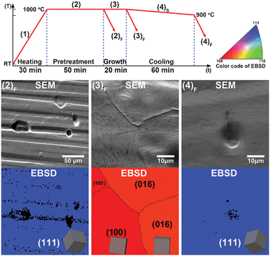 | ||
| Fig. 1 The temperature profile of CVD process and SEM/EBSD results of (2)F heat-treated Cu foil, (3)F fast-cooled graphene/Cu and (4)F slow-cooled graphene/Cu samples. The color code and inset 3D-cubic indicate the lattice orientation of each Cu grain. Under a H2 atmosphere, the heat-treated Cu foil shows a large-area single-crystalline feature Cu(111) orientation, as well as slow-cooled graphene/Cu samples. Sometimes these Cu(111) grains could be as large as a few millimetres. Whereas the Cu in fast-cooled graphene/Cu samples always show poly-crystalline features. | ||
Fig. 2 sketches the mechanism for the proposed evolution of Cu grains in each temperature treatment. The arrows at grain boundaries indicate the directions of grain growth. It is noteworthy that the melting point (m.p.) of pure bulk Cu is ∼1083 °C,26 and the bulk m.p. of the Cu foil we used (99.8%) is lower than this value due to the presence of impurities. Moreover, the surface m.p. of a metal is known to be lower than its bulk m.p.27 Furthermore, the Cu substrates were always slightly vaporized during CVD process and condensed on the inner-surface of quartz tube near the low-temperature zone of furnace (see Supporting Information S2†). This provides evidence that the surface of Cu foil is close to a molten state allowing the migration of Cu atoms and reconstruction of Cu surfaces in the presence of graphene. In other words, instead of graphene preferentially synthesized on a specific Cu crystallographic surface, we can conclude that Cu(100) may be preferentially recrystallized in the presence of a thermally deposited graphene layer. The observation of recrystallized Cu(100)-like orientations upon fast cooling strongly indicates that the presence of graphene is able to kinetically promote the growth of Cu(100). However, the recrystallization of Cu(111) from bulk eventually dominates the structure of the Cu surface if enough time is provided to reach thermodynamically stable states. Noting that the fast-cooled process always results in micro-scaled poly-crystalline Cu(100)-like surface ((3)F in Fig. 1), whereas the case of Cu(111) grains after the slow-cooling process can be as large as a few millimetres ((4)F in Fig. 1). This difference shows that Cu(100) is thermodynamically meta-stable. It is worth noting that the surface recrystallization phenomenon becomes less pronounced if a higher purity Cu foil was used as the substrate. It is due to the fact that its higher m.p. does not allow surface reconstruction at 1000 °C (see Supporting Information S3†).
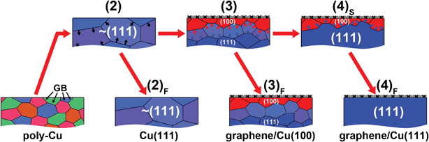 | ||
| Fig. 2 Sketch of Cu grain growth corresponding to different temperature profiles in Fig. 1. The arrows at the grain boundaries (GB) indicate the directions of grain growth. | ||
Formation of Cu2O layer releases the compressive strain from Cu
To reveal the graphene structure on top of various Cu grains, confocal Raman measurements (spot size < 500 nm) were performed. Raman spectroscopy has been widely used to evaluate the number of layers (intensity ratio of I2D/IG and band width of 2D),28 grain size and defect level (intensity ratio of ID/IG).29 The Raman measurements of as-grown graphene were immediately taken after CVD growth. Subsequently, an additional ex-situ step of 3 days ambient oxidation of Cu in air was performed. CVD-grown graphene is polycrystalline in nature,30,31 therefore, ambient oxygen can penetrate through the graphene grain boundaries resulting in a thin Cu oxide layer at the graphene/Cu interface. Naturally if the as-grown graphene has a large domain size (very low density of grain boundaries), the oxidation rate may be very slow.22 In contrast with the slow-cooled sample, the Cu grains of the fast-cooled sample always exhibit poly-crystalline Cu(100)-like features with a small grain size (∼10–100 μm), sometimes a few Cu(111) grains also appear. For this reason we can compare the Raman features of the graphene grown on the sample substrates but sitting on various Cu grains such as graphene/Cu(100) and graphene/Cu(111) before and after 3 days oxidation in air as shown in Fig. 3. Each spectrum is an average of 10 randomly selected sites within the same Cu grain. The peak at ∼540 cm−1, attributed to the formation of Cu2O,32,33 appears after oxidation. We noticed that the D-band (∼1350 cm−1) neither appears nor increases after oxidation, suggesting that the oxidation in air does not significantly increase the defect density on graphene. The Raman 2D-band (at around 2700 cm−1) for the graphene films on Cu(100) and Cu(111) is further red-shifted by 12.9 and 29.4 cm−1, respectively, after oxidation. Meanwhile, the G-band is also red-shifted by about 3.7 and 12.5 cm−1 correspondingly. These observations suggest that the oxygen doping process is not responsible for these shifts because the doping in graphene should induce obvious G-band shift but only small or not appreciable 2D-band shift.34,35 Moreover, a blue-shift in G-band should be expected when graphene is oxidized. Instead, the simultaneous shift of G-and 2D-band implies that the graphene on Cu is more compressively strained compared with those on Cu2O.36 The ratio of the shifts between 2D-and G-band, Δω2D/ΔωG, has been estimated to be around 2.5 if it is caused by hydrostatic pressure,36,37 which is consistent with our experimental values (3.48 for Cu(111) and 2.35 for Cu(100)). It is also obvious that 2D-band becomes narrower after oxidation (from 44 to 29 cm−1 and from 43 to 29 cm−1 of graphene on Cu(111) and Cu(100), respectively). Additionally, the I2D/IG intensity ratio is significantly increased from 1.7 to 3.1 and from 1.6 to 2.9 of graphene on Cu(111) and on Cu(100), respectively. The I2D/IG ∼3 consistent with the reported single-layer CVD graphene on SiO2 substrates.14,16 These observations further indicate that the formation of Cu2O interlayer helps to weaken (or decouple) the graphene-Cu interaction.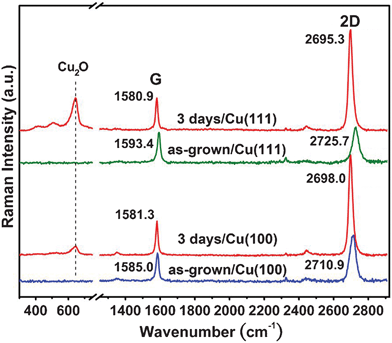 | ||
| Fig. 3 Raman spectra of graphene/Cu(100) and graphene/Cu(111) of fast cooled samples, before and after 3 days oxidation in air. The intensity of the peaks was normalized by the G intensity. | ||
We suggest the origin of such compressive strain was generated during the cooling stage, and a result of the opposite of thermal expansion of Cu (positive expansion coefficient) to the as-grown SLG (negative expansion coefficient).37 This explanation is satisfactory with our results for as-grown SLG on Cu(100) and Cu(111) that show different degrees of Raman shifts due to the difference of in-plane thermal expansion coefficients of the respective orientations. We envisage that, this opposite thermal expansion phenomena between as-grown SLG and specific orientations of Cu substrates may prove useful for strain-engineering of future devices.38
The detailed Raman examination of the graphene films sitting on various Cu grains allows us to conclude that the compressive strain of graphene can be released after the oxidation of the underlying Cu. In order to avoid experimenter-expectancy effect from point-measurements in Fig. 3 (the focused spot size of laser beam is <500 nm), the mapping results of Raman measurement combined with SEM image and EBSD map in Fig. 4 can provide further insight at the micro-scale. Fig. 4a shows a SEM image and its corresponding EBSD map of a fast-cooled graphene/Cu sample with different lattice orientation of Cu(100)-like and Cu(124) in a 40 × 40 μm2 area. The left and right Raman maps in Fig. 4b-f are measurements taken from as-grown and 3 days oxidized sample respectively. The red-shift and width-narrowing of G-and 2D-band (Fig. 4c-f) after 3 days oxidation show a clear dependence of lattice orientation on Cu, as well as the case of slow-cooled samples (see Supporting Information S4†). The graphene/Cu(124) is relatively inert to ambient oxidation (Fig. 4b) which suggests higher surface energy of Cu(124) than Cu(100) and (111).23 Higher surface energy thermodynamically represents higher adhesion force between graphene and Cu, and therefore provides better protection against further oxidation. This also explains the non-apparent shift and width-narrowing of G-and 2D-band of graphene/Cu(124) in Fig. 4.
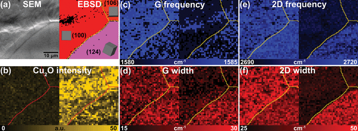 | ||
| Fig. 4 (a) SEM image and its corresponding EBSD map of a fast-cooled graphene/Cu sample with different lattice orientation of Cu(100)-like and Cu(124) in a 40 × 40 μm2 area. Raman maps from the same area correspond to (b) Cu2O intensity, (c) G frequency, (d) G width, (e) 2D frequency and (f) 2D width. The left and right maps in (b)-(f) represent as-grown and 3 days oxidation, respectively. The grain boundaries are indicated by red lines (in Cu2O intensity maps) and yellow lines (in frequency and width maps of G and 2D). | ||
Most importantly, Fig. 3 and Fig. 4 point out that Raman spectra directly taken from as-grown graphene/Cu samples could be misleading, unless the graphene has already been transferred or decoupled. For example, consider the Raman spectra of as-grown SLG/Cu sample in Fig. 3, one may evaluate the graphene as bi-layer to few-layer graphene instead of SLG before graphene was decoupled or transferred. In other words, an additional criterion for quick and convenient identification of coupled-SLG/Cu using Raman spectra is necessary. The row of Decoupled SLG in Table 1 is a criterion for decoupled SLG based on statistics from other studies (see Supporting Information S5†). The decoupled SLG includes exfoliated, transferred to SiO2 and suspended SLG. The as-grown SLG/Cu(100) and as-grown SLG/Cu(111) rows in Table 1 show a suggested criterion for the identification of as-grown SLG on Cu(100) and (111) based on statistics from our results. Table 1 is opened to be enriched for different lattice orientations and substrates. This decoupling phenomenon could also be found in the samples of graphene using thin-film Cu substrates and a cold-wall CVD system (see Supporting Information S6†). Thus we suggest this phenomenon is universal in most CVD cases.
Formation of Cu2O layer weakens the graphene-Cu interaction
Raman spectra have already provided the evidence of the presence of strain. The force curve analysis from scanning probe microscopy could provide further insights about the graphene-Cu interaction. To further corroborate the decoupling phenomenon between graphene and Cu by Cu2O intercalation, we examine a graphene layer on a partially oxidized Cu(111) grain. The distribution of Cu2O over the area is revealed in Fig. 5a (optical image) and 5b (Raman map constructed by plotting Cu2O intensity as the color contrast). Adhesion force and reduced Young's modulus measurements over the whole area were conducted using the peak force mode provided by a close-looped atomic force microscopy (AFM, Dimension ICON, Veeco Instruments Inc.). Fig. 5c is the adhesion force map showing the measured force between Au-coated AFM tip and the sample. The adhesion force measured on the Cu surface is significantly higher than that on Cu2O surface. Meanwhile, the map of the reduced Young's modulus (Fig. 5d) demonstrates that the graphene on Cu is stiffer than that on Cu2O. These results further corroborate that graphene layers have stronger interaction with Cu while the presence of Cu2O significantly reduces this interaction.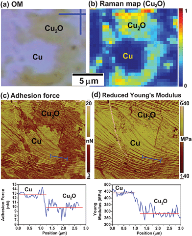 | ||
| Fig. 5 Force curve analysis of SPM on a partially oxidized Cu(111) grain. (a) is the OM image of a partially oxidized Cu(111) area, and (b) is the corresponding Raman map indicating the distribution of Cu2O, (c) and (d) are the adhesion force and reduced Young's modulus maps corresponding to (a) and (b). | ||
Detaching graphene from Cu2O surface
Since as-grown graphene and Cu substrate could be separated by Cu2O intercalation, this result actually provides an alternative way for transferring graphene from Cu surface and the Cu substrates may be re-used. Fig. 6a-c shows a preliminary process for graphene transfer by a selective etching of Cu2O using dilute HCl solution. A PDMS (polydimethylsiloxane) protected graphene/Cu2O/Cu sample was immersed in dilute HCl solution for selective etching of Cu2O. After Cu foil was detached, such Cu foil (Fig. 6d) could be re-used for further graphene synthesis. In our experiments, the quality of 2nd-grown graphene using recycled Cu shows no obvious difference from 1st sample (Fig. 6e). Since the thickness of Cu2O could be controlled (see Supporting Information S7†), in other words, each as-received Cu foil could be re-used for CVD process several times. Note, a uniform, fully-covered Cu2O interlayer is obviously necessary for selective etching, hence the slow-cooled sample (millimetre-scaled Cu(111) dominated) is more suitable for this purpose.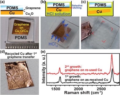 | ||
| Fig. 6 (a)-(c) A preliminary process for transfer of a PDMS protected graphene/Cu2O/Cu sample by a selective etching of Cu2O using dilute HCl solution. (d) The recycled Cu foil after graphene transfer. (e) The Raman spectra of 1st- and 2nd-grown graphene. The quality of 2nd-grown graphene using recycled Cu shows no obvious difference from 1st sample. | ||
Conclusions
In conclusion, we have demonstrated that the cooling process in CVD-grown graphene affects the crystallographic orientation of the Cu grains underlying graphene. Our results show that the graphene induced Cu surface reconstruction favors Cu(100) and the recrystallization of Cu(111) from bulk in fast and slow cooling processes respectively. Therefore, one may need to be cautious when claiming that graphene preferential growth on a specific Cu orientation at process temperatures near the m.p. of metal substrates. On the contrary, in the cases of CVD process using a temperature well below the m.p. of the substrates, more studies are required. From the EBSD/Raman analysis, we have realized that the strong interaction between graphene and Cu can be decoupled by introducing an interlayer of Cu2O between graphene and Cu via a controlled recrystallization and post-oxidation of Cu. The formation of Cu2O at the graphene/Cu interface may be used for transfer of graphene and reuse of Cu foil. The quality of 2nd-growth graphene using recycled Cu shows no obvious difference from 1st graphene. Furthermore, the thickness of Cu2O could be uniformly controlled, and allow the Cu foil to be reused in CVD process several times. This result indicates that the growth of CVD graphene may be more economical by reusing the Cu foil, and the graphene transfer process may be easier by introduction of cuprous oxide intercalation layer.Acknowledgements
This research was supported by Research Center for Applied Science, Academia Sinica (Nano program) and National Science Council Taiwan (NSC-99-2112-M-001-021-MY3, 99-2738-M-001-001 and NSC-98-2218-E-007-003-MY3).References
- K. S. Novoselov, A. K. Geim, S. V. Morozov, D. Jiang, Y. Zhang, S. V. Dubonos, I. V. Grigorieva and A. A. Firsov, Science, 2004, 306, 666–669 CrossRef CAS.
- C.-Y. Su, A.-Y. Lu, Y. Xu, F.-R. Chen, A. N. Khlobystov and L.-J. Li, ACS Nano, 2011, 5, 2332–2339 CrossRef CAS.
- C.-Y. Su, Y. Xu, W. Zhang, J. Zhao, A. Liu, X. Tang, C.-H. Tsai, Y. Huang and L.-J. Li, Acs Nano, 2010, 4, 5285–5292 CrossRef CAS.
- L. J. Cote, F. Kim and J. Huang, J. Am. Chem. Soc., 2008, 131, 1043–1049 CrossRef.
- J. Vaari, J. Lahtinen and P. Hautojärvi, Catal. Lett., 1997, 44, 43–49 CrossRef CAS.
- H. Ueta, M. Saida, C. Nakai, Y. Yamada, M. Sasaki and S. Yamamoto, Surf. Sci., 2004, 560, 183–190 CrossRef CAS.
- J. Coraux, A. T. N'Diaye, C. Busse and T. Michely, Nano Lett., 2008, 8, 565–570 CrossRef CAS.
- S. Marchini, S. Gunther and J. Wintterlin, Physical Review B, 2007, 76 Search PubMed.
- J. Cai, P. Ruffieux, R. Jaafar, M. Bieri, T. Braun, S. Blankenburg, M. Muoth, A. P. Seitsonen, M. Saleh, X. Feng, K. Mullen and R. Fasel, Nature, 2010, 466, 470–473 CrossRef CAS.
- M. Treier, C. A. Pignedoli, T. Laino, R. Rieger, K. Müllen, D. Passerone and R. Fasel, Nat. Chem., 2011, 3, 61–67 CrossRef CAS.
- Y. Gamo, A. Nagashima, M. Wakabayashi, M. Terai and C. Oshima, Surf. Sci., 1997, 374, 61–64 CrossRef CAS.
- A. N. Obraztsov, E. A. Obraztsova, A. V. Tyurnina and A. A. Zolotukhin, Carbon, 2007, 45, 2017–2021 CrossRef CAS.
- Z.-Y. Juang, C.-Y. Wu, A.-Y. Lu, C.-Y. Su, K.-C. Leou, F.-R. Chen and C.-H. Tsai, Carbon, 2010, 48, 3169–3174 CrossRef CAS.
- A. Reina, X. T. Jia, J. Ho, D. Nezich, H. B. Son, V. Bulovic, M. S. Dresselhaus and J. Kong, Nano Lett., 2009, 9, 30–35 CrossRef CAS.
- X. Li, C. W. Magnuson, A. Venugopal, R. M. Tromp, J. B. Hannon, E. M. Vogel, L. Colombo and R. S. Ruoff, J. Am. Chem. Soc., 2011, 133, 2816–2819 CrossRef CAS.
- X. S. Li, W. W. Cai, J. H. An, S. Kim, J. Nah, D. X. Yang, R. Piner, A. Velamakanni, I. Jung, E. Tutuc, S. K. Banerjee, L. Colombo and R. S. Ruoff, Science, 2009, 324, 1312–1314 CrossRef CAS.
- C. Mattevi, H. Kim and M. Chhowalla, J. Mater. Chem., 2011, 21, 3324–3334 RSC.
- S. Bae, H. Kim, Y. Lee, X. Xu, J.-S. Park, Y. Zheng, J. Balakrishnan, T. Lei, H. Ri Kim, Y. I. Song, Y.-J. Kim, K. S. Kim, B. Ozyilmaz, J.-H. Ahn, B. H. Hong and S. Iijima, Nat. Nanotechnol., 2010, 5, 574–578 CrossRef CAS.
- Z. Lee, K. J. Jeon, A. Dato, R. Erni, T. J. Richardson, M. Frenklach and V. Radmilovic, Nano Lett., 2009, 9, 3365–3369 CrossRef CAS.
- X. Dong, Y. Shi, W. Huang, P. Chen and L.-J. Li, Adv. Mater., 2010, 22, 1649–1653 CrossRef CAS.
- J. S. Bunch, A. M. van der Zande, S. S. Verbridge, I. W. Frank, D. M. Tanenbaum, J. M. Parpia, H. G. Craighead and P. L. McEuen, Science, 2007, 315, 490–493 CrossRef CAS.
- S. Chen, L. Brown, M. Levendorf, W. Cai, S.-Y. Ju, J. Edgeworth, X. Li, C. W. Magnuson, A. Velamakanni, R. D. Piner, J. Kang, J. Park and R. S. Ruoff, ACS Nano, 2011, 5, 1321–1327 CrossRef CAS.
- Y.-N. Wen and J.-M. Zhang, Solid State Commun., 2007, 144, 163–167 CrossRef CAS.
- J. M. Wofford, S. Nie, K. F. McCarty, N. C. Bartelt and O. D. Dubon, Nano Lett., 2010, 10, 4890–4896 CrossRef CAS.
- H. I. Rasool, E. B. Song, M. J. Allen, J. K. Wassei, R. B. Kaner, K. L. Wang, B. H. Weiller and J. K. Gimzewski, Nano Lett., 2010, 11, 251–256 CrossRef.
- J. Emsley, The elements, Clarendon Press, 1998 Search PubMed.
- J. W. M. Frenken and J. F. v. d. Veen, Phys. Rev. Lett., 1985, 54, 134 CrossRef CAS.
- A. C. Ferrari, J. C. Meyer, V. Scardaci, C. Casiraghi, M. Lazzeri, F. Mauri, S. Piscanec, D. Jiang, K. S. Novoselov, S. Roth and A. K. Geim, Physical Review Letters, 2006, 97 Search PubMed.
- L. G. Cancado, K. Takai, T. Enoki, M. Endo, Y. A. Kim, H. Mizusaki, A. Jorio, L. N. Coelho, R. Magalhaes-Paniago and M. A. Pimenta, Applied Physics Letters, 2006, 88 Search PubMed.
- P. Y. Huang, C. S. Ruiz-Vargas, A. M. van der Zande, W. S. Whitney, M. P. Levendorf, J. W. Kevek, S. Garg, J. S. Alden, C. J. Hustedt, Y. Zhu, J. Park, P. L. McEuen and D. A. Muller, Nature, 2011, 469, 389–392 CrossRef CAS.
- K. Kim, Z. Lee, W. Regan, C. Kisielowski, M. F. Crommie and A. Zettl, ACS Nano, 2011, 5, 2142–2146 CrossRef CAS.
- H. Dai, C. K. Thai, M. Sarikaya, F. Baneyx and D. T. Schwartz, Langmuir, 2003, 20, 3483–3486 CrossRef.
- M. O'Reilly, X. Jiang, J. T. Beechinor, S. Lynch, C. NíDheasuna, J. C. Patterson and G. M. Crean, Appl. Surf. Sci., 1995, 91, 152–156 CrossRef CAS.
- A. Das, S. Pisana, B. Chakraborty, S. Piscanec, S. K. Saha, U. V. Waghmare, K. S. Novoselov, H. R. Krishnamurthy, A. K. Geim, A. C. Ferrari and A. K. Sood, Nat. Nanotechnol., 2008, 3, 210–215 CrossRef CAS.
- X. Dong, D. Fu, W. Fang, Y. Shi, P. Chen and L.-J. Li, Small, 2009, 5, 1422–1426 CrossRef CAS.
- N. Ferralis, R. Maboudian and C. Carraro, Physical Review Letters, 2008, 101 Search PubMed.
- N. Mounet and N. Marzari, Phys. Rev. B: Condens. Matter Mater. Phys., 2005, 71, 205214 CrossRef.
- F. Guinea, M. I. Katsnelson and A. K. Geim, Nat. Phys., 2010, 6, 30–33 CrossRef CAS.
Footnote |
| † Electronic supplementary information (ESI) available: Raman data, EBDS mappings and results of molecular dynamic calculation are available. See DOI: 10.1039/c2ra01281b |
| This journal is © The Royal Society of Chemistry 2012 |