Synthesis of vertically aligned polyaniline (PANI) nanofibers, nanotubes on APTMS monolayer and their field emission characteristics
Sandip S.
Patil
a,
Shankar P.
Koiry
b,
P.
Veerender
b,
Dinesh K.
Aswal
b,
S. K.
Gupta
b,
Dilip S.
Joag
a and
Mahendra A.
More
*a
aCenter for Advanced Studies in Material Science and Solid State Physics, Department of Physics, University of Pune, Pune-411007, India. E-mail: mam@physics.unipune.ac.in; Fax: +91-20-25691684; Tel: +91-20-25692678
bTechnical Physics Division, Bhabha Atomic Research Center, Trombay, Mumbai, 400 085, India
First published on 11th April 2012
Abstract
Growth of aligned polyaniline (PANI) nanostructures on silicon modified with amino-silane self-assembled (3-aminopropyl)trimethoxysilane (APTMS) monolayer has been carried out by chemical polymerization in the presence of strong (HCl) and weak (CH3COOH) acids as dopant. Self assembly of aniline monomer leading to formation of aligned nanostructures on the APTMS monolayer is due to the amino (–NH2) moieties acting as growth centers. Interestingly, the nature of dopant acid (strong/weak) is found to determine the resultant form of the PANI nanostructures, either as nanofibers or nanotubes. The formation of PANI nanofibers and nanotubes has been revealed by scanning and transmission electron microscopy, whereas confirmation of the conducting phase of PANI is obtained from UV-visible and FTIR analysis. A plausible explanation illustrating the growth mechanism has been presented. Field emission studies of the PANI films have been carried out in a planar diode configuration at base pressure of ∼1 × 10⁻⁸ mbar. The turn-on field required to draw an emission current of 1 nA was found to 1.6 and 2.4 V μm−1 for aligned nanofibers and nanotubes, respectively. Interestingly, both the emitters exhibit good stability of the emission current over a duration of 4 h. The ease of the synthesis route and interesting field emission characteristics indicate the aligned PANI nanofibers and nanotubes as promising materials for field emission based applications.
1 Introduction
One-dimensional (1-D) nanostructures are observed to improve the performance, compactness and sustainability of various field emission based devices; such as high-frequency devices,1 displays,2 vacuum microelectronic devices,3 and in lithography.4 Amongst the innumerable nanomaterials, the inorganic nanostructures of carbon (carbon nanotubes, graphene, diamond etc.),5–7 metal hexaborides (LaB6),8 metal sulfides (GaS, CdS etc.)9,10 and various metal oxide semiconductors (ZnO, TiO2, SnO2etc.)11–13 have been investigated from the field emission point of view. In addition, the nanostructures of organic materials, in particular, conducting polymers (CPs) have attracted a great deal of attention as field emitters, owing to their distinct features such as simple and low cost synthesis, tunable electrical conductivity, etc. The importance of CPs as field emitters was first realized by Musa et al, who have carried out field emission studies of poly(3octylthiophene) films.14 Later on, several groups have investigated the field emission behavior of various CPs, such as PANI, poly(3,4-ethylenedioxythiophene) (PEDOT), polypyrrole (PPy), and their nanocomposites (with carbon nanotubes, metals, metal oxides etc.). Amongst these, Wang et al have reported a field emission of PANI nanofibril array and observed a threshold field of 5–6 V μm−1 for a current density of 0.01 mA cm−2.15 A threshold field of 8–9 V μm−1 (corresponding to an emission current density of 0.01 mA cm−2) has been observed for a copolymer of aniline and pyrrole.16 Kim and his group have performed a good amount of work on field emission from PPy, PANI, PEDOT nanotube and nanowire emitters.17,18 The field emission behavior of PPy nanotubes and nanowires has also been studied by Joo et al19 and Yan et al.20 In order to improve the field emission characteristics of CPs based emitters, attempts have been made to probe the field emission properties their composites with carbon nanotubes, nanoparticles of metals and/or metal oxides.21–23 Recently, we have reported the excellent field emission behavior of chloride-doped PPy and randomly oriented PANI nanotubes.24,25It is well known that, amongst the different CPs, PANI has been the material of choice due to various reasons including ease of synthesis, low cost of monomer, relatively better environmental stability and controlled (tunable) electrical conductivity.26 Various synthesis techniques such as electrochemical or chemical polymerization,27,28 interfacial polymerization,29 plasma polymerization,30 enzymatic polymerization31etc. have been employed for the synthesis of PANI micro/nanostructures. Although the chemical route is most widely used for the synthesis of PANI, it lacks formation of well ordered nanostructures, which are required for specific applications including field emission. The common method employed to synthesise well ordered nanostructures involves the use of hard templates such as anodic aluminium oxide (AAO). Often it is observed that dissolution of the template leads to deterioration of the nanostructures. Furthermore, ‘soft’ template based synthesis does not guarantee well ordered directional growth of the nanostructures.32,33 As a consequence, use of self-assembled monolayers (SAM) to achieve well aligned directional growth is desirable.
In this context, we have demonstrated the synthesis of vertically aligned PANI nanostructures on silicon substrates pre-coated with a SAM of 3-aminopropyltrimethoxysilane [APTMS: NH2(CH2)3Si(OCH3)3].34–36 Since well ordered 1-D nanostructures possessing high aspect ratio are favorable as field emitters, in this paper we report the field emission characteristics of vertically aligned PANI nanotubes and nanofibers synthesized on silicon substrates using a SAM of APTMS. Interestingly, we have observed that the resultant morphology of the PANI nanostructures can be tuned to nanofibers or nanotubes using dopant strong or weak acid. To the best of our knowledge there is no report on the synthesis and field emission of aligned PANI nanotubes using SAM of APTMS.
2 Experimental
2.1 Chemicals
Source chemicals such as APTMS (97% purity), sulfuric acid (H2SO4) and hydrogen peroxide (H2O2) were purchased from Aldrich and used as received. Aniline monomer and acetic acid (CH3COOH) were obtained from Central Drug House LTD, New Delhi, India, while hydrochloric acid (HCl) and ammonium persulfate (APS) ((NH4)2S2O8) were from Thomas Baker, Mumbai and SD Fine-Chem Ltd, Mumbai, India, respectively.2.2 APTMS monolayer deposition on Si-substrate
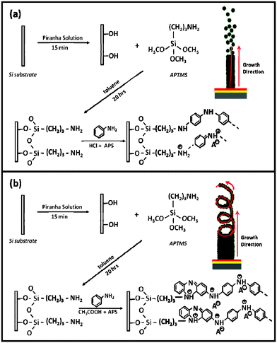
SAMs of APTMS were deposited on hydroxy-terminated native SiO2 surfaces in a glove box (MB 20 G, Mbraun Germany), as per the procedure explained elsewhere.34 In brief, highly doped n type (n++) silicon (resistivity ∼1 mΩ cm) substrates were ultrasonically cleaned in isopropanol and acetone simultaneously followed by deionized water and drying under a stream of N2 jet. The cleaned substrates were dipped into a freshly prepared Piranha solution [H2O2–H2SO4 (1![[thin space (1/6-em)]](https://www.rsc.org/images/entities/char_2009.gif) :1 v/v)] for 15 min. After 15 min, the substrates were removed from the reaction bath and thoroughly cleaned with deionized water several times and dried with N2 gas, so as to remove the excess acid molecules present on the surface. Subsequently, these hydroxylated substrates were transferred to a glove box and immersed in 1 mM APTMS solution (in toluene) for 20 h. After this time, the substrates were cleaned thoroughly by ultrasonication in toluene, isopropanol and acetone to remove any physisorbed molecules. Finally the substrates were washed with deionized water a number of times and dried under a stream of N2.
:1 v/v)] for 15 min. After 15 min, the substrates were removed from the reaction bath and thoroughly cleaned with deionized water several times and dried with N2 gas, so as to remove the excess acid molecules present on the surface. Subsequently, these hydroxylated substrates were transferred to a glove box and immersed in 1 mM APTMS solution (in toluene) for 20 h. After this time, the substrates were cleaned thoroughly by ultrasonication in toluene, isopropanol and acetone to remove any physisorbed molecules. Finally the substrates were washed with deionized water a number of times and dried under a stream of N2.
2.3 Synthesis of PANI on APTMS/Si substrates
For synthesis of PANI nanostructures, the silicon substrates pre-coated with APTMS monolayer (APTMS/Si) were kept in two separate beakers containing 10 mM and 0.2 M aqueous solution of aniline (monomer), respectively. A mixture of 5 mM APS and 1 M HCl was added slowly in the 10 mM aniline solution and the reaction was continued in static condition for 84 h at room temperature.35 In order to reveal the influence of weak acid on the resultant morphology, a mixture of 0.25 M APS and 0.8 M CH3COOH was added slowly in the other beaker containing 0.2 M aniline. This reaction was continued for 12 h in static condition at room temperature. After completion of reaction, the substrates were removed from the dark green suspension. The PANI deposited substrates were washed with a large amount of double distilled water. Since such washing might cause ‘de-doping’ of the films they were exposed to vapours of the respective dopant acids for 2–3 min, followed by drying under a stream of Ar. The schematic of the synthesis process is shown in Scheme 1.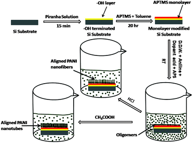 | ||
| Scheme 1 Schematic of synthesis procedure of PANI nanostructures on APTMS/Si. | ||
2.3 Characterization
The synthesized films were characterized by scanning electron microscopy (SEM) (Model-JEOL, JSM 6360A), transmission electron microscopy (TEM) (Model - FEI, Tecnai G2 U20), UV-vis spectrometry (UV-vis) (Model - JASCO, V670) and FTIR spectrometry (Model - JASCO, 6100) to reveal structural, optical and chemical properties.2.4 Field emission studies
Field emission studies were carried out in a planar diode configuration at a base pressure of ∼1 × 10⁻⁸ mbar. The diode configuration comprises of a semi-transparent phosphor screen as an anode and the PANI film on Si substrate as a cathode. The cathodes, one at a time, were pasted on a copper stub connected to a linear motion drive facilitating to-and-fro movement with respect to the anode. The field emission measurements were performed keeping the cathode–anode separation fixed at ∼1 mm. To avoid leakage current, special care was taken using shielded cables and proper grounding during the measurements. The details of vacuum processing and field emission measurements are explained elsewhere.253 Results and discussion
Fig. 1 depicts SEM and TEM images of synthesized PANI films on APTMS/Si substrates using strong and weak dopant acids. Fig. 1a reveals formation of PANI nanofibers uniformly covering the entire substrate surface, as reported earlier.35 The diameter of the PANI nanofibers is estimated to be ∼30–50 nm, with most of them oriented normal to the substrate. Interestingly when the synthesis was performed using weak acid as dopant, a careful observation of Fig. 1b reveals that the PANI nanostructures are tubular rather than fibers. The outer diameter of the PANI nanotubes, estimated from the SEM image, is found to be ∼ 75–100 nm. In order to reveal whether the nanostructures synthesized using weak acid are tubular or not, TEM analysis was performed. A typical TEM image (Fig. 1d) clearly shows the presence of cavities inside the nanofibers confirming formation of nanotubes in the presence of weak acid as a dopant. The diameters of the nanostructures estimated from the TEM images are in good agreement with those derived from SEM analysis. The observed vertical alignment of the PANI nanofibers and nanotubes is due to presence of SAM of APTMS, as described in detail in the earlier report.34 The better vertical alignment of the nanotubes as compared to the nanofibers is attributed to the shorter reaction period. It has been observed that prolonged reaction time leads to formation of longer nanotubes (of several microns) which undergo bending and/or breaking. Thus, the SEM and TEM analysis clearly indicates that the resultant morphology of the PANI nanostructures can be modified from nanofibers to nanotubes by varying the nature of dopant acid.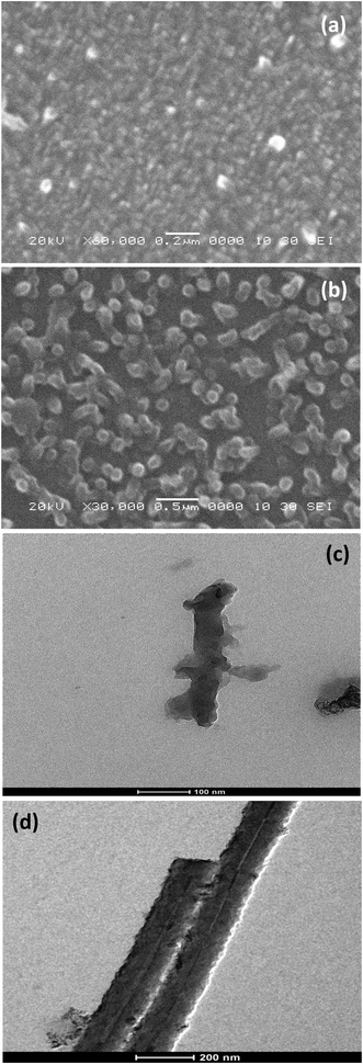 | ||
| Fig. 1 SEM images of (a) PANI nanofibers and (b) PANI nanotubes grown on APTMS/Si. TEM images of (c) PANI nanofibers and (d) PANI nanotubes. | ||
The UV-visible spectra of both the PANI nanostructures (shown in the Fig. 2) exhibit identical spectral features, indicative of conducting phase of PANI. The peaks observed at ∼320–330 and 420–450 nm, are due to the π–π* band transition and the polaron band transition, respectively. The weak broad peak after 800 nm is due to the polaron transition, which is a characteristic of the conducting phase of PANI.37–40 Further, formation of the conducting phase of PANI was confirmed from the FTIR spectra (Fig. 3). The observed spectra are identical to the reported ones, exhibiting peaks at ∼1414 cm−1 (phenazine like unit), 1435 cm−1 (N–H deformation), 1492 cm−1 (C–C modes of benzenoid and quininoid), 1501 cm−1 (C![[double bond, length as m-dash]](https://www.rsc.org/images/entities/char_e001.gif) C stretching of benzenoid), 1537 cm−1 (CC stretching of quininoid) and 1559 cm−1 (quininoid ring deformation).35,41–44 The peaks observed around 1620–1630 cm−1 (marked with circles in Fig. 3b) are due to phenazine units, which are noticeable in this spectrum only. This indicates the vital role played by the phenazine units in formation of the PANI nanotubes when weak acid is used as dopant.45,46
C stretching of benzenoid), 1537 cm−1 (CC stretching of quininoid) and 1559 cm−1 (quininoid ring deformation).35,41–44 The peaks observed around 1620–1630 cm−1 (marked with circles in Fig. 3b) are due to phenazine units, which are noticeable in this spectrum only. This indicates the vital role played by the phenazine units in formation of the PANI nanotubes when weak acid is used as dopant.45,46
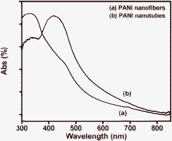 | ||
| Fig. 2 The UV-visible spectra of (a) PANI nanofibers and (b) PANI nanotubes on APTMS/Si. | ||
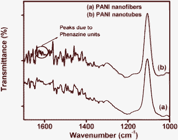 | ||
| Fig. 3 FTIR spectra of (a) PANI nanofibers and (b) PANI nanotubes on APTMS/Si. | ||
A schematic representation of the growth mechanism of the PANI nanostructures on the APTMS monolayer in the presence of different dopant acids is depicted in Scheme 2a and b. As discussed in an earlier report, dipping of cleaned silicon substrates in Piranha solution leads to an –OH terminated surface. When the –OH terminated substrate is dipped in APTMS solution, a self assembly of APTMS molecules occurs via covalent bonding of Si–O–Si polysiloxane reticulation. The self-assembled APTMS monolayer is characterized by –NH2 termination. During polymerization, in presence of the oxidant (APS) these –NH2 groups are converted to radicals (–NH2+), which act as nucleation sites, initiating growth of PANI nanostructures. The role of amino functionalities responsible for the evolution of self organized growth of PANI has been described in earlier reports.34–36 In accordance with this, the possible self organization of oligomers leading to formation of PANI nanofibers in the presence of strong acid (HCl) as dopant, is schematically depicted in Scheme 2a. The formation of nanotubes when weak acid is used as dopant, can be explained as below. It is speculated that the aniline oligomers formed due to oxidation produces phenazine units on the –NH2+ radical sites (as shown in Scheme 2b). These phenazine units then further assemble into columnar structures supported by π–π interactions. The newly generated phenazine units join these columnar structures thereby continuing 1-D growth.25,46 As stated above, it is interesting to note that the appearance of characteristics peaks due to phenazine units is seen only in the FTIR spectrum of PANI nanotubes (Fig. 3b). This indicates that formation of such units is one of the causes responsible for formation of nanotubes, rather than nanofibers under the prevailing experimental conditions.
 | ||
| Scheme 2 Growth mechanism and possible growth direction of (a) PANI nanofibers and (b) PANI nanotubes, on APTMS/Si. | ||
Furthermore, the pH of the reaction medium is observed to be one of the crucial factors governing the resultant growth of the PANI nanostructures. We have studied the variation in pH as a function of time over the entire reaction duration (Fig. 4a and b).
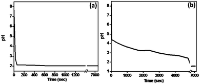 | ||
| Fig. 4 pH variation for polymerization mixture of (a) strong acid (PANI nanofibers) and (b) weak acid (PANI nanotubes). | ||
Fig. 5a depicts the field emission current density vs. applied field (J–E) characteristics of aligned PANI nanofiber and nanotube films. The values of turn-on field, required to draw an emission current of 1 nA, were found to be ∼1.6 and 2.4 V μm−1 for the PANI nanofibers and nanotubes film emitters, respectively. In both cases, with increase in applied voltage, the emission current was seen to increase rapidly, and a current density of 0.01 mA cm−2 was obtained at threshold fields of 2.85 and 3.95 V μm−1 for the PANI nanofibers and nanotubes, respectively.
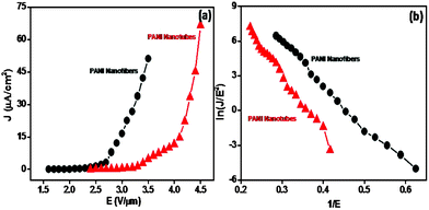 | ||
| Fig. 5 (a) J–E characteristics and (b) F–N plots of PANI nanofibers and nanotubes grown on APTMS/Si. | ||
The values of turn-on and threshold field are observed to be lower than the earlier reported values for PEDOT nanowires, aligned PANI nanofibrils and aniline–pyrrole co-polymer.15–17 Interestingly, the observed values are slightly higher than the previously reported values for PANI nanotubes, synthesized by single-step chemical oxidative polymerization.25Table 1 depicts the comparison of the turn-on and threshold field of different conducting polymers and copolymer with the aligned PANI nanofibers and nanotube films. The variation in the turn-on and threshold field values may be attributed to the different aspect ratios of the PANI nanostructures. Furthermore, the SAM of APTMS may influence the electron transport from substrate to emitter during replenishment. In present studies, the emission current density is estimated by considering the total area of the PANI film.
| Conducting polymer | E to(1 nA)/V μm−1 | E th(1 μA cm−2)/V μm−1 | E th(10 μA cm−2)/V μm−1 | Reference |
|---|---|---|---|---|
| Aligned PANI nanofibers | 1.6 | 2.45 | 2.8 | Present studies |
| Aligned PANI nanotubes | 2.4 | 3.25 | 3.9 | Present studies |
| Aligned PANI nanofibrils | — | — | 5–6 | 15 |
| Aniline–pyrrole co-polymer | — | — | 8–9 | 16 |
| PEDOT nanowires | — | — | 3.5–4 | 17 |
| PANI nanotubes | — | 1.55 | 1.7 | 25 |
The emission current vs. applied field characteristics was analyzed by using the Fowler–Nordheim (F–N) equation,48
| J = A(β2E2/ϕ2)exp(−Bϕ3/2/βE) | (1) |
The stability of field emission current is an important aspect of emission characteristics of a given emitter in the context of its practical applications. The current stability of PANI nanofibers and nanotubes emitters studied at a base pressure of ∼ 1 × 10⁻⁸ mbar, recorded for more than 4 h at the preset value of ∼1 μA, are depicted in Fig. 6a and b. Interestingly, both the emitters exhibit ‘good’ stability of the emission current with ‘spike’ type fluctuations superimposed on it. The fluctuations in the form of ‘spikes’ are due to adsorption, desorption, and/or migration of the residual gas molecules on the emitter surface. The field emission micrographs recorded during stability measurements (given as the inset) show a number of tiny spots, which indicate that the emission is from the most protruding nanofibers and nanotubes.
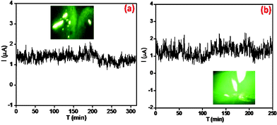 | ||
| Fig. 6 The current–time (I–t) plot of (a) PANI nanofibers and (b) PANI nanotubes on APTMS/Si. The inset shows a field emission micrograph of the respective PANI films. | ||
4 Conclusions
PANI nanofibers and nanotubes have been synthesized on self-assembled APTMS monolayers employing a chemical polymerization route. SEM and TEM analysis clearly reveals formation of vertically aligned PANI nanofibers and nanotubes, when strong (HCl) and weak (CH3COOH) acids are used as dopant, respectively. A plausible growth mechanism is presented, which illustrates the role of pH and phenazine units in the context of nanotube formation. The UV-visible and FTIR spectra confirm formation of the conducting phase of PANI in both cases. The field emission characteristics of the emitters are observed to be promising, exhibiting relatively lower turn-on and threshold field values than reported values and fairly good stability of the emission current. The synthesis approach facilitating modification of morphology of the PANI nanostructures from nanofibers to nanotubes by varying the nature of dopant acid could be explored for the preparation of vertically aligned nanostructures of different materials exhibiting novel functionalities.Acknowledgements
Mr Sandip Patil Acknowledges BARC, Mumbai for financial assistance. M. A. M. would like to thank the BCUD, University of Pune, India for financial support provided for the synthesis and field emission work.References
- K. L. Jensen, R. H. Abrams and R. K. Parker, J. Vac. Sci. Technol., B, 1998, 16(2), 749 CAS.
- C. A. Spindt, C. E. Holland, I. Brodie, J. B. Mooney and E. R. Westerberg, IEEE Trans. Electron Devices, 1989, 36(1), 225 CrossRef CAS.
- M. C. Lin, K. H. Huang, P. S. Lu, P. Y. Lin and R. F. Jao, J. Vac. Sci. Technol., B, 2005, 23(2), 849 CAS.
- A. Kojima, H. Ohyi and N. Koshida, J. Vac. Sci. Technol., B: Microelectron. Nanometer Struct.–Process., Meas., Phenom., 2008, 26(6), 2064 CrossRef CAS.
- C. Li, Y. Zhang, M. Mann, D. Hasko, W. Lei, B. Wang, D. Chu, D. Pribat, G. A. J. Amaratunga and W. I. Milne, Appl. Phys. Lett., 2010, 97, 113107 CrossRef.
- U. A. Palnitkar, V. Kashid Ranjit, A. More Mahendra, S. Joag Dilip, L. S. Panchakarla and C. N. R. Rao, Appl. Phys. Lett., 2010, 97, 063102 CrossRef.
- T. Ikeda and K. Teii, Appl. Phys. Lett., 2009, 94, 143102 CrossRef.
- D. J. Late, V. R. Singh, S. Sinha, M. A. More, K. Dasgupta and D. S. Joag, Appl. Phys. A: Mater. Sci. Process., 2009, 97, 905 CrossRef CAS.
- S. K. Panda, A. Datta, G. Sinha, S. Chaudhuri, P. G. Chavan, S. S. Patil, M. A. More and D. S. Joag, J. Phys. Chem. C, 2008, 112(16), 6240 CAS.
- A. Datta, P. G. Chavan, F. J. Sheini, M. A. More, D. S. Joag and A. Patra, Cryst. Growth Des., 2009, 9(9), 4157 CAS.
- N. Pan, H. Xue, M. Yu, X. Cui, X. Wang, J. G. Hou, J. Huang and S. Z. Deng, Nanotechnology, 2010, 21, 225707 CrossRef.
- Y. Li, X. Fang, N. Koshizaki, T. Sasaki, L. Li, S. Gao, Y. Shimizu, Y. Bando and D. Golberg, Adv. Funct. Mater., 2009, 19, 2467 CrossRef CAS.
- A. B. Bhise, D. J. Late, N. S. Ramgir, M. A. More, I. S. Mulla, V. K. Pillai and D. S. Joag, Thin Solid Films, 2008, 516(18), 6388 CrossRef CAS.
- I. Musa, D. A. I. Munindrasdasa, G. A. J. Amaratunga and W. Eccleston, Nature, 1998, 395, 362 CrossRef CAS.
- C. Wang, Z. Wang, M. Li and H. Li, Chem. Phys. Lett., 2001, 341, 431 CrossRef CAS.
- X. H. Li, W. M. Liu, C. W. Wang and H. L. Li, J. Mater. Sci. Lett., 2003, 22, 1519 CrossRef CAS.
- B. H. Kim, M. S. Kim, K. T. Park, J. K. Lee, D. H. Park, J. Joo, S. G. Yu and S. H. Lee, Appl. Phys. Lett., 2003, 83, 53 Search PubMed.
- B. H. Kim, D. H. Park, J. Joo, S. G. Yu and S. H. Lee, Synth. Met., 2005, 150, 279 CrossRef CAS.
- J. Joo, S. J. Lee, D. H. Park, J. Y. Lee, T. J. Lee, S. H. Seo and C. J. Lee, Electrochem. Solid-State Lett., 2005, 8(4), H39 CrossRef CAS.
- H. Yan, L. Zhang, J. Shen, Z. Chen, G. Shi and B. Zhang, Nanotechnology, 2006, 17, 3446 CrossRef CAS.
- R. B. Rakhi, K. Sethupathi and S. Ramaprabhu, Appl. Surf. Sci., 2008, 254, 6770 CrossRef CAS.
- R. B. Rakhi, K. Sethupathi and S. Ramaprabhu, J. Exp. Nanosci., 2009, 4(1), 67 CrossRef CAS.
- R. Nair, B. Premlal, A. Das and A. K. Sood, Solid State Commun., 2009, 149, 150 CrossRef CAS.
- S. S. Patil, P. Jha, D. K. Aswal, S. K. Gupta, J. V. Yakhmi, D. S. Joag and M. A. More, Polym. Adv. Technol., 2012, 23, 215 CrossRef CAS.
- S. S. Patil, S. P. Koiry, D. K. Aswal, P. M. Koinkar, R. Murakami and M. A. More, J. Electrochem. Soc., 2011, 158(6), E63–E66 CrossRef CAS.
- S. Bhadra, D. Khastgir, N. K. Singha and J. H. Lee, Prog. Polym. Sci., 2009, 34, 783 CrossRef CAS.
- J. Choi, S. J. Kim, J. Lee, J. H. Lim, S. C. Lee and K. J. Kim, Electrochem. Commun., 2007, 9, 971 CrossRef CAS.
- G. R. Li, Z. P. Feng, J. H. Zhong, Z. L. Wang and Y. X. Tong, Macromolecules, 2010, 43, 2178 CrossRef CAS.
- J. Chen, D. Chao, X. Lu and W. Zhang, Mater. Lett., 2007, 61, 1419 CrossRef CAS.
- F. Nastase, I. Stamatin, C. Nastase, D. Mihaiescu and A. Moldovan, Prog. Solid State Chem., 2006, 34, 191 CrossRef CAS.
- R. Cruz-Silva, C. Ruiz-Flores, L. Arizmendi, J. Romero-García, E. Arias-Marin, I. Moggio, F. F. Castillon and M. H. Farias, Polymer, 2006, 47, 1563 CrossRef CAS.
- J. Huang and M. Wan, J. Polym. Sci., Part A: Polym. Chem., 1999, 37, 151 CrossRef CAS.
- (a) Chem. R. V. Parthasarathy and C. R. Martin, Chem. Mater., 1994, 6, 1627 CrossRef; (b) R. Martin, Chem. Mater., 1996, 8, 1739 CrossRef.
- A. K. Chauhan, D. K. Aswal, S. P. koiry, S. K. Gupta, J. V. Yakhmi, C. Surgers, D. Guerin, S. Lenfant and D. Vuillaume, Appl. Phys. A: Mater. Sci. Process., 2007, 90, 581 CrossRef.
- D. S. Sutar, N. Padma, D.K. Aswal, S. K. Deshpande, S. K. Gupta and J.V. Yakhmi, Sens. Actuators, B, 2007, 128, 286 CrossRef.
- D. S. Sutar, N. Padma, D. K. Aswal, S. K. Deshpande, S. K. Gupta and J.V. Yakhmi, J. Colloid Interface Sci., 2007, 313, 353 CrossRef CAS.
- H. Xia, D. Cheng, P. Lam and H. S. O. Chan, Nanotechnology, 2006, 17, 3957 CrossRef CAS.
- H. Ding, M. Wan and Y. Wei, Adv. Mater., 2007, 19, 465 CrossRef CAS.
- J. Xu, K. Wang, S. Z. Zu, B. H. Han and Z. Wei, ACS Nano, 2010, 4(9), 5019 CrossRef CAS.
- J. Han, L. Li and R. Guo, Macromolecules, 2010, 43, 10636 CrossRef CAS.
- Y. G. Wang, H. Q. Li and Y. Y. Xia, Adv. Mater., 2006, 18, 2619 CrossRef CAS.
- P. R. Sajanlal, T. S. Sreeprasad, A. S. Nair and T. Pradeep, Langmuir, 2008, 24, 4607 CrossRef CAS.
- C. Laslau, Z. Zujovic and J. T. Sejdic, Prog. Polym. Sci., 2010, 35, 1403 CrossRef CAS.
- A. Tiwari, R. Kumar, M. Prabaharan, R. R. Pandey, P. kumari, A. Chaturvedi and A. K. Mishra, Polym. Adv. Technol., 2010, 21, 615 CrossRef CAS.
- M. Trchova, I. Syedenkova, E. N. Konyushenko, J. Stejskal, P. Holler and G. Ciric-Marjanovic, J. Phys. Chem. B, 2006, 110, 9461 CrossRef CAS.
- J. Stejskal, I. Sapurina, M. Trchova, E. N. Konyushenko and P. Holler, Polymer, 2006, 47, 8253 CrossRef CAS.
- E. N. Konyushenko, J. Stejskal, I. Sedenkova, M. Trchova, I. Sapurina, M. Cieslar and J. Prokes, Polym. Int., 2006, 55, 31 CrossRef CAS.
- R. H. Fowler and L. Nordheim, Proc. R. Soc. London, Ser. A, 1928, 119, 173 CrossRef CAS.
| This journal is © The Royal Society of Chemistry 2012 |