Facile synthesis of large area porous Cu2O as super hydrophobic yellow-red phosphors†
Satish Laxman
Shinde
and
Karuna Kar
Nanda
*
Materials Research Centre, Indian Institute of Science, Bangalore 560012, India. E-mail: nanda@mrc.iisc.ernet.in; slshinde@mrc.iisc.ernet.in; Fax: +91-80-2360 7316; Tel: +91 080 2293 2996
First published on 2nd March 2012
Abstract
By employing a thermal oxidation strategy, we have grown large area porous Cu2O from Cu foil. CuO nanorods are grown by heating Cu which were in turn heated in an argon atmosphere to obtain a porous Cu2O layer. The porous Cu2O layer is superhydrophobic and exhibits red luminescence. In contrast, Cu2O obtained by direct heating, is hydrophobic and exhibits yellow luminescence. Two more luminescence bands are observed in addition to red and yellow luminescence, corresponding to the recombination of free and bound excitons. Over all, the porous Cu2O obtained from Cu via CuO nanorods, can serve as a superhydrophobic luminescence/phosphor material.
Introduction
Recently phosphor materials have attracted great attention because of their wide spread application in lighting, phosphor thermometry, glow-in-the-dark toys, electroluminescence, white light-emitting diodes (LEDs), cathode ray tubes, etc.1–4 Phosphors are usually made from a suitable host material with an added activator. The host materials are typically oxides, sulfides, selenides, nitrides and oxynitrides.5,6 Many phosphors lose their efficiency gradually by several mechanisms. Absorption of oxygen into oxygen vacancy sites on the surface can change the emission energy of the phosphor.7 Some materials degrade due to the formation of deep traps as water molecules react with the dopant. Therefore, it is desirable to develop a superhydrophobic phosphor for prolonged use.8Generally, metal oxides synthesized by wet chemical methods etc. are hydrophilic because of their surface hydroxyl group. However, they can be made hydrophobic by changing the surface morphology or chemical composition.9–12 Surface roughness is often added to amplify the hydrophobicity of the coating materials. If a surface is rough or microstructured with a low interfacial free energy, the contact angle of water can reach almost 180°.9,13 In this regard, a porous microstructure in luminescent materials can be exceptionally useful. Cu2O is an important p-type semiconductor with a band gap of 2.13 eV that exhibits yellow-orange luminescence.14,15 Porous Cu2O has been synthesized by a wet-chemical reaction route,16 the template synthesis route ,17 and the emulsion synthesis route.18
Here, we report the large area synthesis of super hydrophobic porous films of Cu2O. Cu2O porous films are grown by a two-step process. First, Cu foil is heated in ambient oxygen to obtain CuO nanorods. Then the CuO nanorods film reheated in an Ar atmosphere to form porous Cu2O. The rapid outward and inward diffusion of Cu atoms in the presence and absence of oxygen leads to the porous structure. On the other hand, oxygen diffuses inward in the oxygen atmosphere, but diffuses outward in the absence of oxygen leading to the formation of CuO and Cu2O, respectively. It may be noted that no chemical additive has been used in the fabrication of porous structures. The interesting observations are that Cu2O films are superhydrophobic and exhibit yellow-red luminescence. The large scale synthesis along with the superhydrophobic nature and yellow-red luminescence of oxides can be explored for different potential applications.
Experimental methods
A Cu foil (99.9% purity) is taken in a quartz boat and heated in a horizontal-tube furnace in air and Ar at different temperatures for different durations. CuO nanowires/nanorods are obtained when Cu foil is heated in a tube open at both ends, which then heated in an Ar atmosphere to obtain a porous Cu2O film.Characterization
The morphology and phase of the CuO and the Cu2O films are investigated with scanning electron microscopy (SEM), atomic force microscopy (AFM), X-ray diffraction (XRD), Raman spectroscopy with a 514.5 nm wavelength Ar ion laser and X-ray photoelectron spectroscopy (XPS). The chemical compositions are analysed by XPS and the roughness of film is evaluated by AFM. The hydrophobicity is measured using a GonioStar contact angle system with water. The photoluminescence (PL) spectra are taken with 532 nm laser in the WITec setup.Results
SEM and cross-sectional SEM images shown in Fig. 1(a) and the inset reveal the rod-like morphology obtained by heating Cu foil in air at 550 °C for 4 h in a quartz tube open at both ends. The average diameter and length of the nanorods are ∼300 nm and ∼10 μm, respectively. The X-ray diffraction (XRD) pattern of the nanorods is shown in Fig. S1† which reveals the presence of CuO and Cu2O. When the Cu foil is heated in air at any temperature below 1050 °C,19 Cu2O forms initially due to the oxidation of Cu and then oxidizes to CuO depending on temperature and duration of heat-treatment. This indicates that Cu2O acts as a precursor to the formation of the CuO nanorods. If the temperature, duration and oxygen supply are not enough to fully oxidize Cu2O into CuO, then the sample would be a mixture of both the phases.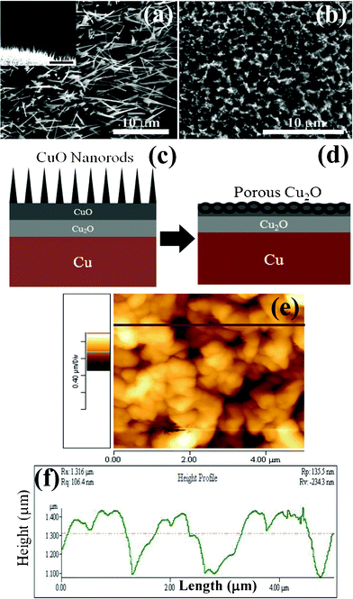 | ||
| Fig. 1 (a) SEM image of the CuO nanorod film obtained at 550 °C for 4 h on Cu foil, inset shows cross sectional SEM image of the film, (b) SEM image of the porous Cu2O film obtained from the CuO nanorods at 600 °C for 2 h, (c) schematic of CuO nanorod formation, (d) schematic of porous Cu2O formation, (e) AFM image of the porous Cu2O film, and (f) height profile of the Cu2O film. | ||
When the film with CuO nanorods is heated in Ar ambient at 600 °C for 2 h, porous film (film I) is obtained as shown in Fig. 1(b). Schematics of the nanorod and porous structures are shown in Fig. 1(c) and (d). Though larger area porous film can be achieved, we were able to design a ∼5 × 5 cm2 porous structure film due to the limitations of our tube furnace. The XRD pattern, Raman spectroscopy and XPS data are shown in Fig. S1–S3†, which confirm the conversion of CuO to Cu2O. The peaks at 932.4 and 933.3 eV correspond to the Cu 2p of Cu2O and CuO, while peaks at 529.3 and 530.9 eV correspond to the O 1s (Fig. S3(a),(b)†). Additional peaks at 531.5, 532.3, 533.3 and 534.4 eV are believed to be due to chemisorbed O− species, and the –O–H bond of adsorbed water on the surface.20Fig. 1(e) and (f) show the AFM image and height profile of the porous Cu2O film, respectively. The pore size is found to be ∼1 μm with an average roughness of ∼100 nm.
In order to investigate the pore formation steps, we have synthesized the porous structures of Cu2O by heating the CuO nanorod film at 600 °C for different durations (Fig. 2). The variation of pore size and pore density with time and temperature for the Cu2O films is shown in Fig. 3(a, b). The pore size is the average of the diameters of several pores, while pore density is the number of pores per unit area. The average pore size obtained at 600 °C for 2 h is ∼ 1.3 μm and the corresponding pore density is ∼6.8 × 108 cm−2. The pore size increases and pore density decreases with temperature and duration of heat-treatment. When the temperature is 650 °C, the pores start to deform into random shapes (Fig. S4) limiting the temperature range. As the temperature and time increase, the diffusion of Cu atoms increases resulting in increased pore size and a reduction in the pore density. The different pore sizes are believed to be due to different diffusion constants.21,22
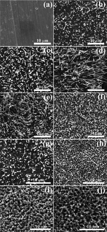 | ||
| Fig. 2 Morphologies obtained by heating Cu under different conditions in a two-step process, (a) Cu foil. CuO nanorods obtained at 550 °C for (b) 1 h, (c) 2 h, (d) 4 h, (e) 6 h. Porous Cu2O obtained from the CuO nanorod film (f) by heating at 600 °C for (g) 0.5 h, (h) 1 h, (i) 1.5 h, (j) 2 h. | ||
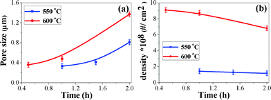 | ||
| Fig. 3 (a) and (b) the variation of pore size and pore density with time at different temperatures for Cu2O. | ||
When Cu foil is heated at high temperature, Cu2O and CuO layers are formed on the Cu foil which act as an interface between the Cu and atmospheric oxygen. The outward diffusion of copper atoms is faster compared to the inward diffusion of oxygen.23 Cu atoms diffuse through the Cu2O layer and react with ambient oxygen, this results in the formation of CuO clusters on the surface.23 The growth continues in the presence of oxygen (when both the ends of the tube are open), which leads to the formation of CuO nanorods. When Cu foil is heated at higher temperatures in a quartz tube closed at both ends, the oxidation stops once all the oxygen is consumed, and there is no nanorod formation. It might be expected that the increase of oxygen content in the atmosphere results in the promotion of an outward diffusion of copper atoms and hence, the formation of longer nanorods24 (Fig. 1(a)) as evinced from Fig. 2(a)–(e).
When the same film of CuO nanorods is heated in an Ar atmosphere, a porous Cu2O film (Fig. 1(b)) is formed as evident from Fig. 2(f)–(j). Under optimum conditions, the CuO nanorods on the Cu foil are completely converted into the porous microstructure of Cu2O which is confirmed by the SEM micrograph shown in Fig. 1(b) and XRD pattern shown in Fig. S1†. The oxidation kinetisc of Cu foil in air as shown in Fig. S5† indicate the increase in weight with time, while the weight increases initially and remains constant in a N2 atmosphere (Fig. S6 and S7†). Isotherm experiments on the CuO nanorods indicate (Fig. S5†) that there is no evaporation of materials. Furthermore, the films CuO nanorods transform to the Cu2O porous structures. Therefore, it is believed that the porous structures are obtained as the nanorods transforms into an island-like structure along with the diffusion of surrounding Cu atoms to fill the voids creating porous structures on the surface as depicted in Fig. 4. The rapid outward diffusion of Cu atoms in the presence of oxygen and the inward diffusion of Cu atoms in the absence of oxygen leads to the porous structure. On the other hand, oxygen diffuses inward in presence of oxygen, while it diffuses outward in the absence of oxygen leading to the formation of Cu2O in a two-step process. This might be a sort of Kirkendall effect.
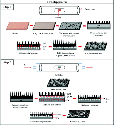 | ||
| Fig. 4 Growth mechanism for porous Cu2O structures. | ||
Fig. 5 shows the variation of contact angle (CA) of water with various morphologies of Cu2O surfaces. As the morphology changes (which changes in the surface roughness), the contact angle changes. The Cu2O film (film II) obtained by removing the CuO nanorods film (CuO nanorods film get exfoliated) synthesized at 550 °C for 4 h shows a contact angle of ∼131° (Fig. 5(a)–(a')). As the nanorod film transforms into the porous film, the surface roughness increases. The presence of air in the pore results in an increase of the contact angle for the porous film.9,10,25 The porous Cu2O (film I) obtained from the CuO nanorod film shows a contact angle of 152° (Fig. 5(b)–(b')). This confirms that the Cu2O film is superhydrophobic in nature. As we vary the annealing temperature, time and gas flow rate during the preparation of the Cu2O films, the surface roughness and chemical composition change. By controlling these parameters, the hydrophobicity of the Cu2O film can be varied. It has been shown for ZnO nanorod films that the wettability of the surface changes from superhydrophobic to superhydrophilic under UV illumination.26 In our case, the contact angle does not change when green laser light is shone on the porous Cu2O film and is believed to be due to the presence of air inside the pores.
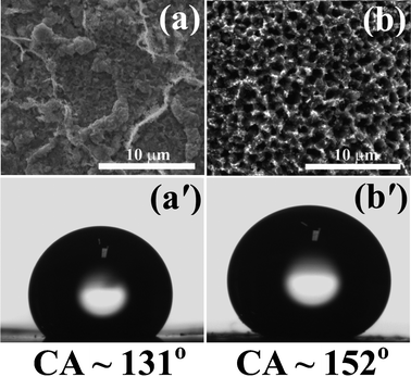 | ||
| Fig. 5 (a) and (b) SEM images and (a') and (b') the contact angles of film II and film I. | ||
Fig. 6(a) and (b) show the PL spectra of both the films I and II. It may be noted that each spectrum can be deconvoluted into three bands. Film II exhibits three bands at 574 nm (2.16 eV), 593 nm (2.09 eV) and 614 nm (2.01 eV) with intense yellow emission (593 nm). Film I also exhibits three bands at 600 nm (2.06 eV), 612 nm (2.02 nm) and 630 nm (1.96 eV) with intense red emission (630 nm). The optical photograph taken by irradiating the sample with 532 nm light also corroborates the yellow and red luminescence as shown in the insets.
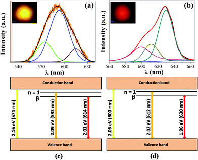 | ||
| Fig. 6 PL spectra of Cu2O film (a) film II and (b) film I. Excitation wavelength is 532 nm. Energy level diagram of Cu2O for (c) film II and (d) film I; n = 1, represents the first excitation line of the yellow series and β represents the excitonic complex due to the n = 1 exciton combined with the level VCu.28 It may be noted that the band gap can vary from sample to sample. | ||
The yellow emission corresponds to a band to band transition, while the red emission corresponds to a recombination process of excitons coupled with impurity centres or stoichiometry defect levels.27,28 Cu2O prepared at higher temperatures can have both Cu and O vacancies and can give a luminescence band in between 610 and 1200 nm.27 Film II is non-porous or less porous and gives yellow luminescence. On the other hand, film I is porous and expected to have more stoichiometry defects. This results in the red luminescence from the porous Cu2O film. The energy level diagram27,28 of Cu2O is shown in Fig. 6(c) and (d). Where n = 1 represents the first excitation line of the yellow series due to free excitons. β is the excitonic complex due to the n = 1 exciton combined with the VCu level,28 which with the valence band yields red emission. In this context, it may be noted that the formation energy of a Cu vacancy is low under any growth conditions29 and it is easy to form Cu vacancies that lead to the p-type nature of Cu2O.
The quantum yield is generally low for Cu2O. However, the luminescence can be enhanced by reducing the pore size or by doping and Cu2O can be used as a superhydrophobic phosphor. We believe that our results will motivate researchers to work in this direction.
Conclusion
We have reported large area synthesis of a superhydrophobic porous Cu2O film by simply heating Cu foil in various atmospheres. It may be noted that no chemical additive is required to obtain porous structure. The Cu2O films exhibit yellow-red luminescence and are either hydrophobic or superhydrophobic depending on the morphology. Because of the combination of properties, porous Cu2O can be used in light emitting devices as superhydrophobic phosphors as well as in other different applications.Acknowledgements
The authors acknowledge Professor S. B. Krupanidhi for providing the AFM and Professor S. Biswas for the GonioStar contact angle system. The authors also acknowledge helpful discussion with Dr S. C. Vanithakumari and C. Saraswathi for her help in the AFM investigation.References
- C. D. S. Brites, P. P. Lima, N. J. O. Silva, A. Milan, V. S. Amarlal, F. Palacio and L. D. A. Carlos, Adv. Mater., 2010, 22, 4499 CrossRef CAS.
- N. Ishiwada, T. Ueda and T. Yokomori, Luminescence, 2011, 26, 381 CrossRef CAS.
- S. Medling, C. France, B. Balaban, M. Kozina, Y. Jiang, F. Bridges and S. A. Carter, J. Phys. D: Appl. Phys., 2011, 44, 205402 CrossRef.
- R.-J. Xie, N. Hirosaki, K. Sakuma, Y. Yamamoto and M. Mitomo, Appl. Phys. Lett., 2004, 84, 5404 CrossRef CAS.
- K. K. Nanda, Key Eng. Mater., 2010, 444, 219 CrossRef.
- R. -J. Xie and N. Hirosaki, Sci. Technol. Adv. Mater., 2007, 8, 588 CrossRef CAS.
- G. Bizarri and B. Moine, J. Lumin., 2005, 113, 199 CrossRef CAS.
- K. H. Lee, S. C. Cho, Y. J. Sung, S. Han, C. U. Bang and D. K. Lee, J. Korean Phys. Soc., 2008, 53, 631 CrossRef CAS.
- F. -M. Chang, S.-L. Cheng, S.-J. Hong, Y.-J. Sheng and H.-K. Tsao, Appl. Phys. Lett., 2010, 96, 114101 CrossRef.
- Y. -J. Sheng, S. Jiang and H.-K. Tsao, J. Chem. Phys., 2007, 127, 234704 CrossRef.
- C. Yang, U. Tartaglino and B. N. J. Persson, Phys. Rev. Lett., 2006, 97, 116103 CrossRef CAS.
- X. Feng, L. Feng, M. Jin, J. Zhai, L. Jiang and D. Zhu, J. Am. Chem. Soc., 2004, 126, 62 CrossRef CAS.
- A. Lafuma and D. Quere, Nat. Mater., 2003, 2, 457 CrossRef CAS.
- H. Solache-Carranco, G. Juarez-Díaz, A. Esparza-García, M. Briseño-García, M. Galván-Arellano, J. Martínez-Juárez, G. Romero-Paredes and R. Peña-Sierra, J. Lumin., 2009, 129, 1483 CrossRef CAS.
- Y. B. Soskovets, A. Y. Khairullina and V. A. Babenko, J. Appl. Spectrosc., 2006, 73, 576 CrossRef CAS.
- P. Sharma and H. S. Bhatti, Mater. Chem. Phys., 2009, 114, 889 CrossRef CAS.
- J. Y. Xiang, X. L. Wang, X. H. Xia, L. Zhang, Y. Zhou, S. J. Shi and J. P. Tu, Electrochim. Acta, 2010, 55, 4921 CrossRef CAS.
- W. Zhang, C. Luan, Z. Yang, X. Liu, D. Zhang and S. Yang, Appl. Surf. Sci., 2007, 253, 6063 CrossRef CAS.
- Y. Zhu, K. Mimura, J.-W. Lim, M. Isshiki and Q. Jiang, Metall. Mater. Trans. A, 2006, 37, 1231 CrossRef.
- D. A. Svintsitskiy, A. I. Stadnichenko, D. V. Demidov, S.V. Koscheev and A. I. Boronin, Appl. Surf. Sci., 2011, 257, 8542 CrossRef CAS.
- R. Nakamura and H. Nakajima, J. Phys.: Conf. Ser., 2008, 165, 12072 CrossRef.
- P. I. Gaiduk, J. L. Hansen and A. N. Larsen, Appl. Phys. Lett., 2008, 92, 193112 CrossRef.
- A. P. Li, F. Muller, A. Birner, K. Nielsch and U. Gosele, Adv. Mater., 1999, 11, 483 CrossRef CAS.
- S. C. Vanithakumari, S. L. Shinde and K. K. Nanda, Mater. Sci. Eng., B, 2011, 176, 669 CrossRef CAS.
- B. Bhushan, Y. C. Jung and K. Koch, Langmuir, 2009, 25, 3240 CrossRef CAS.
- X. Feng, L. Feng, M. Jin, J. Zhai, L. Jiang and D. Zhu, J. Am. Chem. Soc., 2004, 126, 62 CrossRef CAS.
- T. Ito and T. Masumi, J. Phys. Soc. Jpn., 1997, 66, 2185 CrossRef CAS.
- M. Zouaghi, B. Prevot, C. Carabatos and M. Sieskind, Phys. Status Solidi A, 1972, 11, 449 CrossRef CAS.
- H. Raebiger, S. Lany and A. Zunger, Phys. Rev. B: Condens. Matter Mater. Phys., 2007, 76, 045209 CrossRef.
Footnote |
| † Electronic Supplementary Information (ESI) available. See DOI: 10.1039/c2ra20066j/ |
| This journal is © The Royal Society of Chemistry 2012 |