Meniscus coated high open-circuit voltage bi-layer solar cells
Olga
Malinkiewicz
,
Martijn
Lenes
,
Hicham
Brine
and
H. J.
Bolink
*
Instituto de Ciencia Molecular, Universidad de Valencia, PO Box 22085, ES-46071, Valencia, Spain. E-mail: henk.bolink@uv.es
First published on 16th January 2012
Abstract
Neat bi-layer solar cells of a fullerene acceptor and a cyanine dye donor were prepared using meniscus coating. Meniscus coating is very material efficient and leads to high quality pinhole-free films. The cells exhibit high open circuit voltages of 1 volt, only 0.8 eV below the band gap of the cyanine dye. This is one of the smallest differences reported for organic solar cells and illustrates an almost optimal donor–acceptor energy level alignment.
Introduction
The field of organic photovoltaics (OPV) has been receiving considerable attention ever since the invention of the bi-layer type solar cell by Tang in 1986.1 There, a sandwich structure consisting of two materials with a band-edge offset was used to split up strongly bound excitons into free carriers leading to the first reasonably efficient organic solar cell. Throughout the years a steady increase in efficiency has been obtained using this type of solar cell by optimizing energy levels, electrode materials, carrier mobilities and absorption coefficients leading to power conversion efficiencies of over 3%.2 Higher device efficiencies are generally reported for bulk heterojunction (BHJ) devices, formed by phase separated donor and acceptor molecules.3 Although pioneered for polymeric donor materials, BHJs have also been prepared using evaporated materials.4,5 This when used in combination with doped transport layers has led to a device efficiency of 8.3%.6,7 BHJ solar cells are still dominated by polymeric donor materials in combination with a small molecular weight solution processable fullerene derivative.8,9 One drawback related to the use of polymers is their complex synthesis and associated difficult purification. Alternatively, small molecular weight materials can also be used as donors and have led to promising solution processable BHJ devices.10,11 The high efficiencies obtained with BHJ architectures exist due to a much larger donor–acceptor interface enabling thicker films. These structures, however, are at the same time difficult to control as they depend critically on the dimensions and extension of each of the two phases which is altered by the choice of solvent, processing conditions and annealing of the film. This holds especially for small molecule based BHJs which often show a very fine intermixing of donor and acceptor greatly increasing recombination losses. Therefore, there is still an interest to prepare planar donor–acceptor junctions as it allows for a better understanding of the device mechanisms.2,12–14 Additionally, it serves as a platform to screen materials in a more straightforward way as the device performance can be considered a minimum achievable value. Planar devices are usually prepared by vacuum deposition as this ensures a well-defined interface between the two layers. Partial solution processed devices have also been reported in which the first material, usually the donor is processed from solution and the second material is deposited on top via vacuum sublimation.15 Recently, neat double layer devices were prepared using a film transfer method that revealed interesting device physics.16 It is in general not trivial to obtain a bi-layer device of only small molecular weight materials using solution processing.Here we demonstrate solution processed neat bi-layer inverted solar cells using cationic cyanine dyes as the electron donor and a functionalized fullerene derivative as the electron acceptor. Cyanine dyes are interesting candidates for use in solar cells because of their very high absorption coefficients (105 M−1 cm−1) allowing a large number of photons to be absorbed in extremely thin layers.15,17–19 Secondly they are soluble in polar solvents and exhibit good film forming properties. This enables their solution based processing on top of a film consisting of a functionalized fullerene soluble in aromatic solvents. Lastly, they are commercially available in a great number of varieties enabling fine-tuning of energy levels and physical properties.
Results and discussion
For this study two dyes, 1-ethyl-2-[3-(1-ethyl-3,3-dimethyl-1,3-dihydro-indol-2-ylidene)-propenyl]-3,3-dimethyl-3H-indolium hexafluorophosphate (D1) and 3-butyl-2-[3-(3-butyl-1,3-dihydro-1,1-dimethyl-2H-benzo[e]indol-2-ylidene)-propenyl]-1,1-dimethyl-1H-benzo[e]indolium perchlorate (D2), were used as donors (Fig. 1 left). The acceptor used in this study, [6,6]-phenyl-C61-butyric acid methyl ester (PCBM) is a functionalized fullerene which is one of the most studied materials in OPV because of its high carrier mobility, appropriate energy levels for forming a type II heterojunction with most available donor materials, and high solubility. | ||
| Fig. 1 Chemical structure of the cyanine dyes and their thin film absorption spectra (left) and energy of the work function, valence and conduction band and molecular orbitals for the electrodes, metal oxides and organic molecules, respectively (right). | ||
The cationic cyanine dyes dissolve well in polar solvents, such as 2,2,3,3-tetrafluoro-1-propanol (TFP). Unfortunately, they also dissolve, albeit only at low concentrations, in the aromatic solvents (toluene, chlorobenzene) used to process PCBM. Therefore, it is not possible to obtain neat bi-layers by processing PCBM on top of the cyanine dye based film, as a fraction of the dye would dissolve and mix with the PCBM layer. PCBM, however, is completely insoluble in TFP and therefore it should be possible to deposit the cyanine dyes on top of the PCBM layer. Hence an inverted device structure is required for this solution processed bi-layer solar cell. In order to achieve efficient charge collection buffer layers are used, ZnO in between the ITO and the PCBM layer and molybdenum trioxide (MoO3) in between the metal and the cyanine dye layer (Fig. 1 right). The use of MoO3 offers advantages over the more commonly used PEDOT:PSS as hole injection/extraction layer due to the deep lying HOMO levels of the cyanine dyes.13 Secondly the ZnO/active layer/MoO3 device architecture has been proven to be a stable configuration offering high performance and lifetimes in inverted photovoltaic and light emitting devices.20
We have employed a non-standard method to deposit the small molecular weight materials based films referred to as meniscus coating.21 In our lab-scale method we use capillary forces to place the drop of solution containing the small molecular weight molecules in between the substrate and the bottom of a flat blade (3 by 20 mm). Because the distance between the blade and the substrate is small (0.2 mm) the drop is maintained within the gap creating the so called meniscus. This meniscus is stretched when moving the blade over the substrate leaving behind a thin film of the small molecular weight material (Fig. 2).
 | ||
| Fig. 2 Schematic of the meniscus coating technique employed. | ||
The resulting dry film thickness is primarily determined by the drawing speed of the blade and its distance to the substrate.22 This is different from blade coating where the solution is pushed by the blade leaving behind a thick wet film (the thickness depending on the height of the blade used).
A solution (30 μl) containing 0.24 mg of PCBM in chlorobenzene was used to coat a 50 nm thick PCBM film on an ITO/ZnO substrate 3 cm wide and 12 cm long, the drawing speed of the blade was 20 mm s−1. The resulting PCBM layer is very uniform and shows a rms of around 2 nm from AFM analysis (Fig. 3A). To compare this PCBM film quality with spin coated ones, PCBM layers were also prepared by spin coating from a chlorobenzene solution using concentrations of 20 and 30 mg ml−1. By varying the rotation speed of the spin coater, PCBM films with a thickness of 50 nm could be obtained for both concentrations. These spin coated layers also appear quite homogeneous with an rms below 3 nm (Fig. 3B) yet show a considerable amount of pinholes penetrating through the layer. Such pinholes are highly undesirable since they will result in the generation of shorts and hinder the formation of a neat bi-layer. These pinholes were present in all the spin coated films prepared and not observed in any of the meniscus coated films.
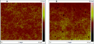 | ||
| Fig. 3 Atomic force microscope images of A: PCBM film coated using meniscus coating and B: PCBM film coated using spin coating. | ||
After preparing the PCBM layer by meniscus coating and a short drying period (20 s) the dye layer is applied using meniscus coating. In order to create a neat bi-layer the solvent of the dye should not dissolve the underlying PCBM layer. The integrity of the PCBM layer upon exposure to TFP by the meniscus coating was verified by comparing the absorption spectrum of the film before and after exposure (Fig. 4). From these measurements it was established that the coating procedure does not change the underlying PCBM layer and a neat PCBM/dye solution processed bi-layer is formed. The solution processed bi-layer architecture was completed to a photovoltaic cell by thermally evaporating the MoO3 and Ag layers. An additional benefit of meniscus-coating above spincoating is the very low material usage as most of the solution is used for the film formation. In contrast, with spincoating typically only 5% of the material ends up in the film. To prepare a 50 nm thick layer on our 30 by 30 mm substrates using spincoating 6.7 mg PCBM was needed whereas with meniscus coating we employed only 0.24 mg.
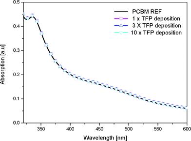 | ||
| Fig. 4 Thickness profiles and absorption spectra of PCBM films exposed to TFP solutions. | ||
To identify the optimum performance, solar cells with different layer thicknesses of the PCBM and D1 were prepared. The layer thicknesses used were 45, 50 and 70 nm for the PCBM layer and 30, 40 and 30 nm for the dye layer. These layers were integrated in the following devices A, B and C, having PCBM and D1 layer thicknesses of 45 and 30 nm, 50 and 40 nm, and 70 and 30 nm, respectively. We note that meniscus coating allows to accurately prepare films with varying thicknesses. The J–V curves obtained for these devices under white light illumination are depicted in Fig. 5.
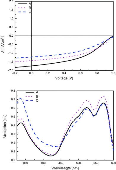 | ||
| Fig. 5 J–V curves for devices A, B and C under white light illumination (top) and the corresponding absorption spectra (bottom). | ||
The absorption spectra of the devices resemble the layer thickness, that is, the device with the thinnest layers has the lowest absorption. Interestingly, the maximum current density is obtained for the device with the thinnest layers of PCBM and cyanine dye (45 and 30 nm, respectively). This is likely due to the limited exciton diffusion length in the materials, meaning that while the thicker dye layer is able to absorb more photons, the additionally generated excitons do not reach the donor–acceptor interface and hence do not contribute to the device current. For practical reasons it is difficult to go to a thinner cyanine dye layer which might be required to reduce the recombination losses and hence lead to higher fill factors. The performance for these cells is summarized in Table 1.
| PCBM [nm] | Dye [nm] | IPCE [%] | PE [%] | FF [%] | V oc [V] | J sc [mA cm−2] | J sc corrected[mA cm−2] | |
|---|---|---|---|---|---|---|---|---|
| A | 45 | 30 | 15 | 0.6 | 0.43 | 1 | 1.7 | 1.5 |
| B | 50 | 40 | 13 | 0.59 | 0.46 | 1 | 1.42 | 1.28 |
| C | 70 | 30 | 10 | 0.45 | 0.41 | 1 | 1.2 | 1 |
For this reason layer thicknesses of 45 nm for the PCBM and 30 nm for the cyanine dye layers were selected for further device analysis using both dyes, D1 and D2.
The typical absorption spectra of both the bi-layer devices are depicted in Fig. 6. The absorption in the visible region is governed by the cyanine dyes. Both devices show similar absorption intensities yet the absorption spectrum of the device employing D2 is red-shifted by approximately 50 nm in accordance with the absorption spectra of the pure dyes and its narrower bandgap. The highest incident photon-to-current conversion efficiencies (IPCE) are around 15% and coincide with the peak in the absorption of the cyanine dyes. For non-inverted device geometries the IPCE spectrum can show a dip at the absorption peak of the dye. This is related to the extremely high absorption coefficient of the dyes resulting in most of the light being absorbed in the first few nanometres of the dye layer, which in that case is at the donor–anode interface. For these inverted bi-layers however this phenomenon called antibatic behaviour does not occur since the light enters the donor layer at the donor–acceptor interface.13
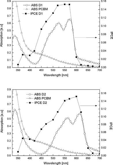 | ||
| Fig. 6 Typical absorption spectrum (open symbols) and IPCE versus wavelength (solid squares) for the bi-layer solar cells, employing D1 (top) and employing D2 (bottom), additionally the absorption spectrum of a PCBM film is depicted. | ||
The IPCE as a function of wavelength follows the absorption spectra over the range of the solar spectrum with contributions of both dye and fullerene.
White light J–V characteristics for the bi-layer at around 1 sun illumination are depicted in Fig. 7 and the main performance parameters are depicted in Table 2.
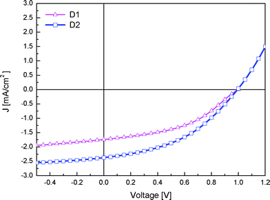 | ||
| Fig. 7 J–V curves for the bi-layer solar cells with dyes D1 and D2 under white light illumination. | ||
| Dye | PCBM [nm] | Dye [nm] | IPCE [%] | PE [%] | FF [%] | V oc [V] | J sc [mA cm−2] | J sc corrected[mA cm−2] |
|---|---|---|---|---|---|---|---|---|
| D1 | 50 | 30 | 15 | 0.6 | 0.43 | 1 | 1.7 | 1.5 |
| D2 | 50 | 30 | 15 | 0.7 | 0.42 | 0.99 | 2.4 | 1.7 |
The achieved open circuit voltages (Voc) (1.0 and 0.99 V) are especially high for organic solar cells. Previous reports of solar cells using cyanine dyes showed limited voltages of 0.6–0.7 V caused by the mismatch of the deep lying HOMO level of the dyes with the work function of PEDOT:PSS. The open circuit voltages we observed are even higher compared to devices using a vacuum dried polyaniline anode (Voc = 0.72 V).13 The difference of the Voc and the bandgap (1.8 eV) is especially for the cell employing D2 rather small at 0.8 eV. This is one of the smallest differences reported for organic solar cells and illustrates an almost optimal energy level alignment.23,24 As D1 absorbs at shorter wavelengths its energy gap is slightly larger and as such the energy difference between the Voc and the band gap is around 1 eV. The short circuit current (Jsc) reaches 1.5 and 1.7 mA cm−2 for the devices using D1 and D2, respectively where the narrower band gap of D2 ensures a better overlap with the solar spectrum and hence facilitates higher currents.
We note that the devices presented in this paper are fabricated using commercially available starting materials which are used without further purifying. Especially for the cyanine dyes, higher purity starting materials are expected to increase the performance considerably by increasing the exciton diffusion lengths and carrier mobilities. For example it was shown by Fan et al. that EQEs of 60% can be reached using similar cyanine dyes in a bi-layer heterojunction with C60.13
Conclusions
In summary solution processed bi-layer solar cells are demonstrated using small molecular weight materials. Meniscus coating was used to prepare the neat bi-layer devices as this technique allows for high quality pinhole-free films with very small material usage. Efficiencies of 0.6% are obtained with exceptionally high open circuit voltages of 1 volt demonstrating the optimal alignment of donor and acceptor energy levels.Experimental details
Prepatterned ITO-covered glass substrates (http://www.naranjosubstrates.com/) were extensively cleaned using detergent, demineralised water, and isopropyl alcohol, respectively, followed by UV-ozone treatment. The 30 nm ZnO layer was obtained by spin coating a precursor solution onto the cleaned substrates followed by an annealing step at 400 °C for 3 h. The precursor solution used was a solution containing zinc acetate dehydrate and acetic acid dissolved in ethanol![[thin space (1/6-em)]](https://www.rsc.org/images/entities/char_2009.gif) :
:![[thin space (1/6-em)]](https://www.rsc.org/images/entities/char_2009.gif) water (3
water (3![[thin space (1/6-em)]](https://www.rsc.org/images/entities/char_2009.gif) :
:![[thin space (1/6-em)]](https://www.rsc.org/images/entities/char_2009.gif) 1). Acetic acid was added to avoid the formation of zinc hydroxide, Zn(OH)2, and to enhance the film quality. A 50 nm layer of PCBM (SOLENME) was prepared by meniscus coating using a chlorobenzene solution (20 mg ml−1) (technique described above) followed by the deposition of a 30 nm dye layer (FEW CHEMICALS) from a TFP solution (7 mg ml−1) using the same technique. The samples were transferred to a nitrogen filled glove box (1 ppm O2 and <1 ppm H2O) where 30 nm MoO3/70 nm silver top contact were thermally evaporated (<5 × 10⁻⁶ mbar).14 Solar cells (active area 9 mm2) were illuminated by a white light halogen lamp in combination with interference filters for the EQE and J–V measurements (MiniSun simulator by ECN the Netherlands). An estimation of the short-circuit current density (Jsc) under standard test conditions was calculated by convolving the EQE spectrum with the AM1.5G reference spectrum, using the premise of a linear dependence of Jsc on light intensity. J–V characteristics of the solar cells were recorded using a Keithley 2400 SourceMeter. All characterisation was performed in a nitrogen filled glove box (1 ppm O2 and <1 ppm H2O).
1). Acetic acid was added to avoid the formation of zinc hydroxide, Zn(OH)2, and to enhance the film quality. A 50 nm layer of PCBM (SOLENME) was prepared by meniscus coating using a chlorobenzene solution (20 mg ml−1) (technique described above) followed by the deposition of a 30 nm dye layer (FEW CHEMICALS) from a TFP solution (7 mg ml−1) using the same technique. The samples were transferred to a nitrogen filled glove box (1 ppm O2 and <1 ppm H2O) where 30 nm MoO3/70 nm silver top contact were thermally evaporated (<5 × 10⁻⁶ mbar).14 Solar cells (active area 9 mm2) were illuminated by a white light halogen lamp in combination with interference filters for the EQE and J–V measurements (MiniSun simulator by ECN the Netherlands). An estimation of the short-circuit current density (Jsc) under standard test conditions was calculated by convolving the EQE spectrum with the AM1.5G reference spectrum, using the premise of a linear dependence of Jsc on light intensity. J–V characteristics of the solar cells were recorded using a Keithley 2400 SourceMeter. All characterisation was performed in a nitrogen filled glove box (1 ppm O2 and <1 ppm H2O).
Acknowledgements
This work has been supported by the European Union FP7 program (ORION, 229036), the Spanish Ministry of Science and Innovation (MICINN) (MAT2011-24594, CSD2007-00010) and the Generalitat Valenciana. The authors greatly acknowledge Alejandra Soriano, Jorge Ferrando and Eva Tormos for device preparation and testing, technical assistance and AFM analysis, respectively.References
- C. W. Tang, Appl. Phys. Lett., 1986, 48, 183 CrossRef CAS.
- R. Fitzner, E. Reinold, A. Mishra, E. Mena-Osteritz, H. Ziehlke, C. Koerner, K. Leo, M. Riede, M. Weil, O. Tsaryova, A. Weiss, C. Uhrich, M. Pfeiffer and P. Bauerle, Adv. Funct. Mater., 2011, 21, 897 CrossRef CAS.
- G. Dennler, M. Scharber and C. J. Brabec, Adv. Mater., 2009, 21, 1323 CrossRef CAS.
- P. Peumans, S. Uchida and S. R. Forrest, Nature, 2003, 425, 158 CrossRef CAS.
- A. Ojala, H. Bürckstümmer, M. Stolte, R. Sens, H. Reichelt, P. Erk, J. Hwang, D. Hertel, K. Meerholz and F. Würthner, Adv. Mater., 2011, 23, 5398 CrossRef CAS.
- http://www.heliatek.com/news-19 .
- M. Riede, T. Mueller, W. Tress, R. Schueppel and K. Leo, Nanotechnology, 2008, 19, 424001 CrossRef CAS.
- S. H. Park, A. Roy, S. Beaupre, S. Cho, N. Coates, J. S. Moon, D. Moses, M. Leclerc, K. Lee and A. J. Heeger, Nat. Photonics, 2009, 3, 297–303 CrossRef CAS.
- G. Yang, Y. Yang, L. Yu, Y. Wu and G. Li, Nat. Photonics, 2009, 3, 649–653 CrossRef.
- Y. Liu, X. Wan, F. Wang, J. Zhou, G. Long, J. Tian and Y. Chen, Adv. Mater., 2011, 23, 5387 CrossRef CAS.
- B. Walker, C. Kim and T. Nguyen, Chem. Mater., 2011, 23, 470–482 CrossRef CAS.
- M. Lenes and H. J. Bolink, ACS Appl. Mater. Interfaces, 2010, 2, 3664 CAS.
- B. Fan, F. Araujo de Castro, B. T. Chu, J. Heier, D. Opris, R. Hany and F. Nuesch, J. Mater. Chem., 2010, 20, 2952–2955 RSC.
- X. Tong, B. E. Lassiter and S. R. Forrest, Org. Electron., 2010, 11, 705–709 CrossRef CAS.
- B. Fan, R. Hany, J. Moser and F. Nuesch, Org. Electron., 2008, 9, 85–90 CrossRef CAS.
- A. Tada, Y. Geng, Q. Wei, K. Hashimoto and K. Tajima, Nat. Mater., 2011, 10, 450 CrossRef CAS.
- X. Ma, J. Hua, W. Wu, Y. Jin, F. Meng, W. Zhan and H. Tian, Tetrahedron, 2008, 64, 345–350 CrossRef CAS.
- P. Bouit, D. Rauh, S. Neugebauer, J. L. Delgado, E. Di Piazza, S. Rigaut, O. Maury, C. Andraud, V. Dyakonov and N. Martin, Org. Lett., 2009, 11, 4806 CrossRef CAS.
- C. Villegas, E. Krokos, P. Bouit, J. L. Delgado, D. M. Guldi and N. Martin, Energy Environ. Sci., 2011, 4, 679 CAS.
- J. Wang, W. Weng, M. Tsai, M. Lee, S. Horng, T. Perng, C. Kei, C. Yu and H. Meng, J. Mater. Chem., 2010, 20, 862 RSC.
- C. S. Herrick, Ind. Eng. Chem. Prod. Res. Dev., 1980, 19, 314–316 CrossRef CAS.
- J. A. Britten, Chem. Eng. Commun., 1993, 120, 59–71 CrossRef CAS.
- D. Veldman, S. C. J. Meskers and R. A. J. Janssen, Adv. Funct. Mater., 2009, 19, 1939 CrossRef CAS.
- P. Heremans, D. Cheyns and B. P. Rand, Acc. Chem. Res., 2009, 42, 1740–1747 CrossRef CAS.
| This journal is © The Royal Society of Chemistry 2012 |
