Phenanthroline diimide as an organic electron-injecting material for organic light-emitting devices†
Hyena
Lee‡
a,
Gwijeong
Cho‡
ab,
Sungho
Woo
ac,
Sungho
Nam
a,
Jaehoon
Jeong
ac,
Hwajeong
Kim
*ad and
Youngkyoo
Kim
*a
aOrganic Nanoelectronics Laboratory, Department of Chemical Engineering, Kyungpook National University, Daegu 702-701, Republic of Korea. Fax: +82 53 950 6615; Tel: +82 53 950 5616
bOLED Device Development Team, LG Display Co., Ltd., Gumi City 730-030, Republic of Korea
cGreen Energy Research Division, DGIST, Daegu 711-873, Republic of Korea
dPriority Research Center, Research Institute of Advanced Energy Technology, Kyungpook National University, Daegu 702-701, Republic of Korea. E-mail: ykimm@knu.ac.kr; khj217@knu.ac.kr; Web: http//one.knu.ac.kr
First published on 26th July 2012
Abstract
We report a diimide-type organic electron-injecting material, bis-[1,10]phenanthrolin-5-yl-pyromellitic diimide (Bphen-PMDI), for organic light-emitting devices (OLEDs), which was synthesized from its monomers, pyromellitic dianhydride (PMDA) and 1,10-phenanthrolin-5-amine (PTA). The vacuum-purified Bphen-PMDI powder showed high glass transition (∼230 °C) and thermal decomposition (∼400 °C) temperatures, whereas neither melting point nor particular long-range crystal nanostructures were observed from its solid samples. The optical band gap energy and the ionization potential of the Bphen-PMDI film were 3.6 eV and 6.0 eV, respectively, leading to the lowest unoccupied molecular orbital (LUMO) energy of 2.4 eV. Inserting a 1 nm thick Bphen-PMDI layer between the emission layer and the cathode layer improved the device current density by 10-fold and the luminance by 6-fold, compared to the OLED without the Bphen-PMDI layer. The result suggests that an effective electron tunnel injection process occurs through the Bphen-PMDI layer.
Introduction
Recently organic light-emitting devices (OLEDs) have been successfully commercialized for high-definition full-colour displays which are mostly adapted to smart (mobile) phones, even though monochromatic or low-resolution OLED display products have been launched since 1997.1–5 Commercializing these high-resolution full-colour OLED displays implies that most problems including lifetimes and/or colour stability issues in the OLED structure are resolved at least for small-size displays.6–8 However, large-size OLED displays for monitors and televisions are still under development because of immature technology for effective heat-sinking control (spot-heating leading to gradual colour change or unbalanced lifetime for individual pixels), large-area coating (uniformity), etc.To speed up the commercialization of large-size OLED displays, various efforts have been attempted such as simplification of OLED unit device structures (by reducing the number of organic layers to secure the thickness uniformity of each organic layer) and replacement of inorganic electron-injecting materials (lithium fluoride – LiF, etc.) with organic electron-injecting materials (to fit similar evaporation conditions).9–13 Here we note that various coordination complexes such as lithium 8-hydroxyquinoline (Liq) and a modified diphenylvinyl benzene derivative have been developed as an electron-injecting materials but their performances could not exceed the LiF performance in terms of luminous efficiency at high current density.2–13 In our previous report, we found that a diimide nanocluster could play the hole-trapping and electron-injecting roles.13 However, the OLED devices in the previous study did still contain the inorganic electron-injecting layer (LiF) so that the electron-injecting role of diimide nanoclusters was more or less ambiguous. In addition, the diimide in our previous work has an aliphatic center group (bicyclooctene unit) that has no sufficient conjugated pathway for electron transport even in the localized diimide molecule.
Hence, in this work, we synthesized a new diimide material, bis-[1,10]phenanthrolin-5-yl-pyromellitic diimide (Bphen-PMDI), that has a rigid aromatic (i.e., phenyl) ring in the center unit as well as an electron-deficient (i.e., accepting) phenanthroline unit.14 To evaluate the Bphen-PMDI material as an electron-injecting layer (EIL), we fabricated OLED devices by replacing the LiF layer with the Bphen-PMDI layer. Device results showed that the electron injection from the cathode into the emission layer was greatly improved by the presence of the 1 nm thick Bphen-PMDI layer.
Results and discussion
The Bphen-PMDI material was synthesized from pyromellitic dianhydride (PMDA) and 1,10-phenanthrolin-5-amine (PTA) via an imidization reaction in N,N-dimethylacetamide (DMAc) solvent (Fig. 1a). The imidization reaction was carried out by a two-step process for high yield: (1) chemical imidization in the presence of triethylamine (TEA) and (2) thermal imidization at the solvent reflux temperature. At the early stage of the chemical imidization step at lower temperatures, the amic acid intermediate (bis-[1,10]phenanthrolin-5-yl-pyromellitamic acid (Bphen-PMDA)) was formed and was still soluble in DMAc. When the imidization reaction proceeded, white solids were formed in the solution. By further heating up to the reflux temperature of DMAc, the precipitated product became pronouncedly enriched in the reaction solution. The final obtained product (Bphen-PMDI) was a white solid (see details in the experimental section).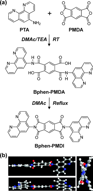 | ||
| Fig. 1 (a) Synthesis procedure of Bphen-PMDI via Bphen-PMDA intermediate and (b) energy minimized structures of Bphen-PMDI depending on the viewing direction by using the MM2 program (ChemBio3D, CambridgeSoft). TEA and DMAc denote triethylamine and N,N-dimethylacetamide, respectively. | ||
As shown in the energy minimized structures (Fig. 1b), the two phenanthroline units are not in the same plane so that the molecular stacking (ordering) of Bphen-PMDI molecules is expected to be relatively loose in the perpendicular direction of the longer molecular axis (i.e., the line between two phenanthroline units). This loose packing can lead to a low crystallinity for the Bphen-PMDI bulk materials, even though the single Bphen-PMDI molecule has a low degree of freedom in terms of rotation of constituent chemical groups inside the molecule for thermal transition of the molecule owing to the rigid molecular structure in the presence of two large and twisted phenanthroline units.
The thermal properties of the synthesized Bphen-PMDI powders were measured as shown in Fig. 2. As shown in Fig. S1a†, the thermogravimetric analysis (TGA) measurement showed that the weight loss at relatively low temperatures (150–200 °C) was ∼20% for the Bphen-PMDI powders that were purified by only wet processes (see details in the experimental section). In addition, a broad endothermic peak was measured at 200–300 °C from the differential scanning calorimetry (DSC) thermogram (see the inset in Fig. S1a†). Therefore the TGA and DSC results of the materials purified by only wet processes indicate that there are unwanted materials in the product powders when the wet purification process was applied only. Hence we carried out a vacuum purification (sublimation) process at above 300 °C, which resulted in further purified product with a major thermal degradation temperature of ∼400 °C (Fig. 2a) and a glass transition temperature (Tg) of ∼230 °C (Fig. 2b and the Fig. S2b inset for another measurement run†). It is also noteworthy that no melting peak was measured even though the temperature was increased up to the degradation temperature (onset = ∼400 °C).
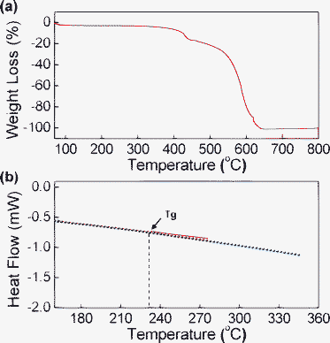 | ||
| Fig. 2 TGA (a) and DSC (b) thermograms of Bphen-PMDI powders after vacuum purification (sublimation): the “Tg” point denotes the onset position of the glass transition. | ||
Next, the nanostructure of the vacuum-purified Bphen-PMDI powders was examined using high resolution transmission electron microscopy (HRTEM) and powder X-ray diffraction (XRD) techniques. As shown in the HRTEM image (Fig. 3a), no particular crystal lattices were observed but only random powder patterns appeared, although the maximum resolution was applied (see also Fig. S2†). However, the XRD diffractogram showed quite well-defined diffraction peaks. Considering the length of PMDI and phenanthroline units, the peaks at the angles larger than 2θ = 37° (d-spacing < 0.24 nm) can be assigned to the diffraction of atomic bond units in the Bphen-PMDI when it comes to the C–C and/or C![[double bond, length as m-dash]](https://www.rsc.org/images/entities/char_e001.gif) C bond lengths.15 On the other hand, the rest peaks (at the angles smaller than 2θ = 37°) are considered to be related with the diffractions of PMDI and phenanthroline units. In particular, the peak “1” (d-spacing = 0.8 nm) can be assigned to the intermolecular distance in the direction perpendicular to the long axis of the Bphen-PMDI molecule, because the maximum size (long axis) of the phenanthroline unit is about 0.7 nm (between the 3-position carbon and the 8-position carbon) and 0.9 nm (between the 3-position hydrogen and the 8-position hydrogen) and the two phenanthroline units are twisted leading to less stacking (see also Fig. 1b) (note that the long axis size of Bphen-PMDI is larger than 2 nm). So, from the HRTEM and XRD results, we can briefly conclude that the Bphen-PMDI molecules in solid states have a short range ordering but no long range ordering leading to highly ordered crystalline phases.
C bond lengths.15 On the other hand, the rest peaks (at the angles smaller than 2θ = 37°) are considered to be related with the diffractions of PMDI and phenanthroline units. In particular, the peak “1” (d-spacing = 0.8 nm) can be assigned to the intermolecular distance in the direction perpendicular to the long axis of the Bphen-PMDI molecule, because the maximum size (long axis) of the phenanthroline unit is about 0.7 nm (between the 3-position carbon and the 8-position carbon) and 0.9 nm (between the 3-position hydrogen and the 8-position hydrogen) and the two phenanthroline units are twisted leading to less stacking (see also Fig. 1b) (note that the long axis size of Bphen-PMDI is larger than 2 nm). So, from the HRTEM and XRD results, we can briefly conclude that the Bphen-PMDI molecules in solid states have a short range ordering but no long range ordering leading to highly ordered crystalline phases.
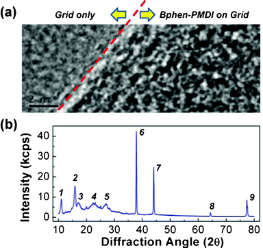 | ||
| Fig. 3 (a) HRTEM image of Bphen-PMDI powders on a Cu-grid (the scale bar is 2 nm) and (b) powder XRD diffractogram of Bphen-PMDI powders: d-spacing = 0.8 nm (peak 1), 0.56 nm (2), 0.53 nm (3), 0.4 nm (4), 0.33 nm (5), 0.24 nm (6), 0.21 nm (7), 0.14 nm (8), 0.12 nm (9). | ||
Based on the nanostructure information of the vacuum-purified Bphen-PMDI powders, we measured the optical and photoelectronic characteristics of the Bphen-PMDI thin films that were coated on quartz substrates by thermal evaporation in a vacuum. As shown in Fig. 4a, the absorption edge of the Bphen-PMDI film reached ∼400 nm in the presence of major absorption below ∼350 nm. The onset point of absorption was 345 nm leading to an optical band gap of 3.6 eV. A weak photoluminescence (PL) was measured for the Bphen-PMDI film at a wavelength of ∼405 nm (maximum). The actual PL observation from the Bphen-PMDI film reflects that the Bphen-PMDI molecules are less tightly packed (stacked) than the highly ordered (stacked) imide derivatives including aromatic polyimides because they exhibit almost no PL in solid states by making a charge transfer complex.16,17 This result is in good agreement with the HRTEM and XRD data as discussed in Fig. 3. Therefore we can shortly summarize that the present Bphen-PMDI film is optically transparent in the visible light range and has a high glass transition temperature (in spite of loose molecular packing), which supports its strong suitability for stable OLED applications. As shown in Fig. 4b, the photoelectron (PE) yield of the Bphen-PMDI film was quite low compared to that of well-known p-type (electron-donating) materials.18,19 The onset point of the PE yield was 5.75 eV, which can be calculated to the real ionization potential of 6.0 eV after calibration.18–21 From the optical band gap and ionization potential (highest occupied molecular orbital – HOMO), we can get 2.4 eV as the lowest unoccupied molecular orbital (LUMO) energy of the Bphen-PMDI film.
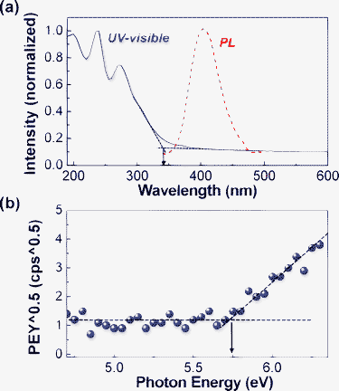 | ||
| Fig. 4 (a) UV-visible and PL spectra of the Bphen-PMDI film on quartz substrates and (b) PE yield spectrum of the Bphen-PMDI film on a glass substrate. Arrows denote the onset points of each spectrum. | ||
Using the vacuum-purified Bphen-PMDI material as an electron-injecting layer (instead of a typically used LiF layer), we fabricated multilayer-type OLEDs as shown in Fig. 5a. To examine the performance of Bphen-PMDI as an EIL, a well-proven undoped green emission layer (tris(8-hydroxyquinolinato)aluminium (Alq3)) (EML) was employed.22–25 4,4′,4′′-tris(N-(2-naphthyl)-N-phenylamino) triphenylamine (2TNATA) and N,N′-bis(naphthalen-1-yl)-N,N′-bis(phenyl)benzidine (NPB) were used as a hole-injecting layer (HIL) and a hole-transporting layer (HTL), respectively.23–25
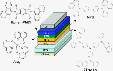 | ||
| Fig. 5 Schematic illustration of the multilayer-type OLED structure and chemical structures of organic materials used for each layer. | ||
As shown in the flat energy band diagram of the multilayer OLED structure (Fig. 6a), the LUMO energy level of the Bphen-PMDI layer is higher (relative to the work function of Al) than that of the Alq3 layer. This energy level difference resembles the case of LiF,1,2,11 which means the existence of a large electron barrier between the EML (Alq3) and the cathode (Al). For proper functioning of OLEDs, hence, an electron tunnelling process should be made through the Bphen-PMDI layer (Fig. 6b). Here we need to pay attention to the polar carbonyl groups in the Bphen-PMDI layer, which are expected to play a similar dipole role as for the LiF case.26 Here we note that a local (short-range) ordering is still present in the Bphen-PMDI even though it is not a highly ordered material. If the dipole effect does not work, it is supposed that the electron injection from the cathode (Al) does not happen. To understand the electron tunnelling action in the present OLEDs, the thickness of the Bphen-PMDI layer was controlled precisely up to 3 nm as similarly applied for the LiF case.1,11,27
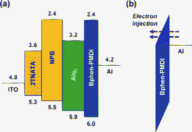 | ||
| Fig. 6 (a) Flat energy band diagram of the OLED with the Bphen-PMDI layer and (b) schematic illustration of the electron tunnelling process through the LUMO level of the Bphen-PMDI layer. Note that the minus sign and ‘eV’ units were omitted for each number. | ||
The current density–voltage (J–V) characteristics of OLEDs are shown in Fig. 7a. A diode-like current increase was observed for all devices, which indicates that the electron tunnelling was apparently successful through the Bphen-PMDI LUMO level in the multilayer devices. In particular, the increase of current density became higher as the Bphen-PMDI thickness increased up to 1 nm. The current density of the device with the 1 nm-thick Bphen-PMDI layer was about 10-fold higher compared to that of the device without the Bphen-PMDI layer (control device) at 10 V. This result reflects that the presence of the Bphen-PMDI layer (∼1 nm thick) greatly improved the electron injection performance in the devices. However, further increase of the Bphen-PMDI thickness led to a gradual decrease in the current density. When the thickness of the Bphen-PMDI layer became 2 nm, the current density of the device with the Bphen-PMDI layer was even lower than that of the control device. This trend is similar to the case of the LiF layer which exhibited an optimal thickness of around 1 nm.1,11,27
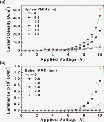 | ||
| Fig. 7 J–V (a) and L–V (b) characteristics of OLEDs according to the thickness of the Bphen-PMDI layer. | ||
As shown in the luminance–voltage (L–V) characteristics (Fig. 7b), the luminance of the device with the 1 nm-thick Bphen-PMDI layer was increased by ca. 6-fold compared to that of the control device. This can be also attributed to the enhanced electron injection through the Bphen-PMDI layer to the Alq3 layer (EML). Interestingly, as the Bphen-PMDI thickness increased up to 2 nm, the luminance was considerably decreased to less than 100 cd m−2 at 10 V. The extent of the luminance reduction was much larger than that of the current density reduction, which can be ascribed to the shifted recombination zone toward the Bphen-PMDI layer owing to the increased electron retardation by the thicker Bphen-PMDI layer. However, we note that the emission colour was almost not changed with the Bphen-PMDI layer thickness (see Fig. S3†).
As shown in Fig. 8a, the luminous efficiency was increased as the luminance increased for the three representative devices (note that the initial trend of the device with the 1 nm-thick Bphen-PMDI layer was slightly different as shown in Fig. S4†). Although the luminance was always higher for the device with the 1 nm-thick Bphen-PMDI layer than that with the 0.5 nm-thick Bphen-PMDI layer, the luminous efficiency was flipped (the 0.5 nm-thick device showed higher efficiency over the entire luminance range). This result implies that the current injection became much higher for the 1 nm-thick device than the 0.5 nm-thick device, suggesting further improvement in device performances by the fine control of the Bphen-PMDI layer thickness. Summarizing the device performance, the maximum luminance was achieved for the device with the 1 nm-thick Bphen-PMDI layer (Fig. 8b). In particular, the voltage required for 100 cd m−2 was greatly reduced when the Bphen-PMDI layer (0.5 nm and 1 nm thick) was introduced in between the emission layer and the cathode, which indicates the improved electron injection by the presence of the Bphen-PMDI layer. Here a particular attention is paid to the still higher performance of the device with the 0.5 nm-thick Bphen-PMDI layer compared to the control device, whereas the device performance was extremely poor for the devices with the 2 nm or 3 nm-thick Bphen-PMDI layer.
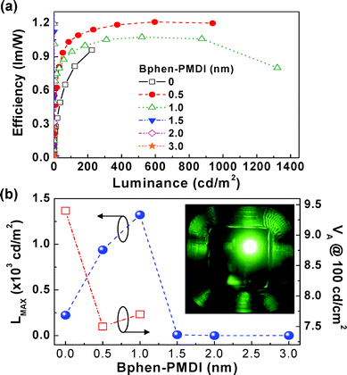 | ||
| Fig. 8 (a) Luminous efficiency as a function of luminance for the OLEDs with the Bphen-PMDI layers, (b) maximum luminance (left) and voltage at 100 cd m−2 (right) as a function of the Bphen-PMDI layer thickness (the inset shows a photograph of green emission from the OLED with the 1 nm-thick Bphen-PMDI layer). | ||
Finally, we tried to briefly examine the performance of the Bphen-PMDI layer compared to the LiF layer. As shown in Fig. S5a and S5b†, the current injection and luminance characteristics at a fixed voltage were slightly worse for the Bphen-PMDI layer than the LiF layer. However, we found that the Bphen-PMDI layer has an advantage in the luminous efficiency, though a further detailed comparison should be carried out with better optimized device structures (Fig. S5c†).
Conclusions
The diimide-type organic electron-injecting material, Bphen-PMDI, was synthesized by a two step imidization process. The vacuum-purified Bphen-PMDI powder showed high thermal decomposition (onset point = ∼400 °C) and glass transition (onset point = ∼230 °C) temperatures but did not exhibit any melting point. Although the powder XRD measurement showed a diffraction peak, no particular nanostructures (such as crystal lattices by long-range ordering) were found from the HRTEM images. This result indicates that the Bphen-PMDI material is thermally stable without a pronounced intermolecular crystallization, which is expected to be suitable for securing the long-term stability of OLEDs. The optical band gap energy of the Bphen-PMDI film was 3.6 eV, while its ionization potential (HOMO energy) was 6.0 eV. As a result, the LUMO energy was calculated to be 2.4 eV. The performance of multilayer OLEDs was noticeably improved as the Bphen-PMDI layer thickness increased up to 1 nm, but it decreased again by further increasing the Bphen-PMDI layer thickness. This trend was explained by the enhanced electron injection (tunnelling process) as observed similarly in the LiF case. The current density and the luminance of the devices with the 1 nm-thick Bphen-PMDI layer were improved by ca. 10-fold and 6-fold, respectively. However, higher luminous efficiency was achieved for the 0.5 nm-thick Bphen-PMDI layer. It is particularly noteworthy that the driving voltage was remarkably reduced by inserting the 0.5 nm or 1 nm-thick Bphen-PMDI layer. This result supports the effective electron tunnelling function of the present Bphen-PMDI layer as a possible replacement for the conventional inorganic electron-injecting material (LiF) that has intrinsically poor adhesion (interaction) to organic layers.Experimental section
Materials and synthesis:
Pyromellitic dianhydride (PMDA) and 1,10-phenanthrolin-5-amine (PTA) were purchased from Sigma-Aldrich and used without further purification. N,N-dimethylacetamide (DMAc, Sigma-Aldrich) was subject to dehydration using molecular sieves, while triethylamine (TEA, Sigma-Aldrich) was used as received. To synthesize the Bphen-PMDI material, PMDA (0.825 g, 3.75 mmol) and PTA (1.68 g, 8.625 mmol) were added to a three-necked flask charged with DMAc (25 ml) under continuous stirring. To this reactant solution TEA (0.11 ml) was added at room temperature. At this step, all reactants became slowly dissolved in the solvent, indicating the gradual formation of amic acid moieties (Bphen-PMDA). After ca. 4 h, there were some particles generated in the solution. Then the reaction temperature was increased up to the reflux condition of DMAc, which resulted in the gradual generation of bigger white particles. After terminating the reaction, the solution was poured drop-wise into denionized (DI) water to remove DMAc and some unreacted residues. This process delivered a white solid product and then was subject to a repeated washing–precipitation procedure with DMAc and DI water until the colour of DMAc and water phases was unchanged. This wet-purified product was dried in a vacuum oven at ca. 80 °C for 48 h. The final yield of the Bphen-PMDI powder was 70% (see Fig. S6 and S7 for the mass spectrum†). The elemental analysis result of Bphen-PMDI (C34H16N6O4): (calculated) C (71.3%), H (2.8%), N (14.7%), O (11.2%); (measured) C (71.1%), H (2.9%), N (14.4%), O (11.6%) (we note that the powder sample was subject to a degassing process using a vacuum sample holder in order to remove oxygen molecules included during sampling). The major solid-state 13C-NMR peaks were found at δ = 166.2 ppm (PMDI unit), 136.5 ppm (PMDI unit), 126.2 ppm (PMDI unit), 150.7 ppm (phenanthroline unit), 145.5 ppm (phenanthroline unit) (see details in Fig. S8†). We note that a liquid-state NMR measurement was impossible because of poor solubility of Bphen-PMDI powder in any organic solvents (see Fig. S9†).Film and device fabrication:
For the measurement of optical and photoelectronic properties, the Bphen-PMDI film (30 nm thick) was deposited on quartz or glass substrates by thermal evaporation in a vacuum. To fabricate OLEDs, indium-tin oxide (ITO)-coated glass substrates (sheet resistance = 10 Ω/□) were patterned by a photolithography technique to have 12 mm × 8 mm ITO stripes, followed by wet (acetone and isopropyl alcohol) and dry (UV–ozone) cleaning processes. The cleaned ITO-glass substrates were loaded into a vacuum chamber that is connected to a nitrogen-filled glove box. After pumping the chamber pressure down to ∼1 × 10⁻⁶ Torr, organic layers were deposited step by step: HIL (2TNATA, t = 40 nm), HTL (NPB, t = 30 nm), EML (Alq3, t = 30 nm), and EIL (Bphen-PMDI, t = 0, 0.5, 1.0, 2.0, 3.0 nm). Then the cathode (Al, t = 100 nm) was deposited without breaking vacuum, which defined the device active area of 3 mm × 3 mm. These devices were kept inside the glove box before measurement in order to avoid any attack from oxygen and/or moisture.Simulation and measurement:
The energy minimized structure of the Bphen-PMDI material was obtained by the simulation using the MM2 program in the ChemBio3D module (CambridgeSoft): the heating/cooling rate was set as 1 kcal/atom, while the target temperature was set as 300 K. The synthesized Bphen-PMDI material was characterized by a matrix-assisted laser desorption time-of-flight mass spectrometer (MALDI-TOF-MS, Voyager DE-STR, Applied biosystems), a solid-state 13C-NMR (Unity Plus INOVA 600 MHz (14.1 Tesla), Varian), and an element analyzer (EA, Flash 2000, ThermoFisher). The thermal decomposition and glass transition temperatures were measured using a thermogravimetric analyzer (TGA, Q600, TA Instruments) and a differential scanning calorimeter (DSC, Q2000, TA Instruments), respectively. The nanostructure of the Bphen-PMDI powders was measured using a high-resolution transmission electron microscope (HRTEM, Tecnai G2 F20 S-TWIN, PHILIPS) and a X-ray diffractometer (XRD, D/Max-2500, Rigaku). A copper (Cu) grid (300 mesh, 3 mm diameter, Veco Square Mesh) was used to prepare samples for the HRTEM measurement. The optical absorption and photoluminescence spectra of the Bphen-PMDI film was measured using a UV-visible spectrometer (Optizen 2120+, Mecasys Co., Ltd) and fluorescence spectrometer (FP-6500, JASCO), respectively. A photoelectron yield spectrometer (PEYS, AC-2, Riken Keikki) was used to measure the ionization potential of the Bphen-PMDI film. The J–V and L–V characteristics of the OLEDs were measured using a specialized OLED measurement system equipped with an electrometer (Keithley 238) and a candelameter (CS1000, Minolta).Acknowledgements
This work was financially supported by Korean Government grants (Basic Research Laboratory Program_2011_0020264, Priority Research Center Program_2009-0093819, Pioneer Research Center Program_2011-0001646, NRF_2010-0004164, NRF_2012-000523).References
- L. S. Hung and C. H. Chen, Mater. Sci. Eng., R, 2002, 39, 143 CrossRef.
- Y. Kim and C. S. Ha, Advances in Organic Light-Emitting Device, Trans Tech Publications, Switzerland, 2008 Search PubMed.
- S. H. Hwang, C. N. Moorefield and G. R. Newkome, Chem. Soc. Rev., 2008, 37, 2543 RSC.
- Y. Tao, C. Yang and J. Qin, Chem. Soc. Rev., 2011, 40, 2943 RSC.
- H. Fu, Y.-M. Cheng, P.-T. Chou and Y. Chi, Mater. Today, 2011, 14, 472 CrossRef CAS.
- Y. Kim, D. Choi, H. Lim and C. S. Ha, Appl. Phys. Lett., 2003, 82, 2200 CrossRef CAS.
- Y. Kim, K. H. Bae, Y. Y. Jeong, D. K. Choi and C. S. Ha, Chem. Mater., 2004, 16, 5051 CrossRef CAS.
- M. O′Regan, Dig. Tech. Pap. - Soc. Inf. Disp. Int. Symp., 2009, 40, 600 CrossRef.
- G. He, O. Schneider, D. Qin, X. Zhou, M. Pfeiffer and K. Leo, J. Appl. Phys., 2004, 95, 5773 CrossRef CAS.
- R. Meerheim, B. Lussem and K. Leo, Proc. IEEE, 2009, 97, 1606 CrossRef CAS.
- L. S. Hung, C. W. Tang and M. G. Mason, Appl. Phys. Lett., 1997, 70, 152 CrossRef CAS.
- Y. Kim, D. Choi, B. Moon, E. Oh, H. Lim, S. Kwon and C.-S. Ha, Adv. Eng. Mater., 2005, 7, 1023 CrossRef CAS.
- S. Lee, K. Sethuraman, J. An and C. Im, Journal of the Korean Physical Society, 2012, 60, 849 CrossRef CAS.
- G. Cho, H. Lee, S. Woo, S. Nam, H. Kim and Y. Kim, Nanoscale, 2011, 3, 1073 RSC.
- U. Couhorn and R. Dronskowski, J. Inorg. Gen. Chem., 2004, 630, 427 CAS.
- M. K. Ghosh and K. L. Mittal, in Polyimides: Fundamentals and Applications, Marcel Dekker, Inc., New York, 1996 Search PubMed.
- S. Ando, J. Photopolym. Sci. Technol., 2004, 17, 219 CrossRef CAS.
- H. Kim, M. Shin and Y. Kim, Macromol. Res., 2009, 17, 445 CrossRef CAS.
- M. Shin, H. Kim and Y. Kim, Mater. Sci. Eng., B, 2010, 176, 382 CrossRef.
- S. Nam, M. Shin, H. Kim, C.-S. Ha, M. Ree and Y. Kim, Adv. Funct. Mater., 2011, 21, 4527 CrossRef CAS.
- S. Nam, S. Lee, I. Lee, M. Shin, H. Kim and Y. Kim, Nanoscale, 2011, 3, 4261 RSC.
- C. W. Tang and S. A. Vanslyke, Appl. Phys. Lett., 1987, 51, 913 CrossRef CAS.
- T. Tsutsui, E.-I. Aminaka, Y. Fujita, Y. Hamada and S. Saito, Synth. Met., 1993, 57, 4157 CrossRef CAS.
- Y. Shirota, Y. Kuwabara, D. Okuda, R. Okuda, H. Ogawa, H. Inada, T. Wakimoto, H. Nakada, Y. Yonemoto, S. Kawami and K. Imai, J. Lumin., 1997, 72–74, 985 CrossRef CAS.
- Y. Kim, D. Choi and H. Kim, The Open Physical Chemistry Journal, 2008, 2, 13 CrossRef CAS.
- H. Heil, J. Steiger, S. Karg, M. Gastel, H. Ortner, H. Von Seggern and M. Stöβel, J. Appl. Phys., 2001, 89, 420 CrossRef CAS.
- Y. Kim, Nanotechnology, 2008, 19, 355207 CrossRef.
Footnotes |
| † Electronic supplementary information (ESI) available: TGA/DSC thermograms, TEM images, EL spectra, logarithmic plot of luminous efficiency, device performance comparison data between Bphen-PMDI and LiF, MALDI-TOF-MS spectrum, NMR spectrum. See DOI: 10.1039/c2ra20524f |
| ‡ These authors contributed equally to this work. |
| This journal is © The Royal Society of Chemistry 2012 |
