Efficient flexible dye-sensitized solar cells fabricated by transferring photoanode with a buffer layer
Xizhe
Liu
ab,
Long
Wang
a,
Zhaosheng
Xue
a and
Bin
Liu
*ac
aDepartment of Chemical and Biomolecular Engineering, National University of Singapore, Singapore, 117576. E-mail: cheliub@nus.edu.sg
bInstitute of Atomic and Molecular Physics, JiLin University, ChangChun, P.R. China
cInstitute of Materials Research and Engineering, 3 Research Link Singapore 117602
First published on 25th May 2012
Abstract
An efficient organic dye sensitized TiO2 flexible photoanode with a TiO2 dense buffer layer was fabricated by a transferring technique. The photoanode has good inter-layer connection and the resultant device exhibits low recombination.
Flexible dye-sensitized solar cells (DSSCs) on plastic substrates are advantageous in having light weight and high deformability, which are desirable for portable applications.1–3 As electrolytes and Pt electrodes are readily flexible, the fabrication of high quality TiO2 porous electrodes on flexible substrate becomes the key challenge.
TiO2 porous electrode is composed of nanometer size particles. The interconnection between these nanoparticles is important for electron transport. In general, a good connection between TiO2 nanoparticles is produced by high temperature sintering at 450 °C to 500 °C to form mesoporous structures on glass substrates. As plastic substrates cannot withstand such a high temperature, several low temperature processing methods have been developed.4,5 Compression is one of the often used techniques for treatment of TiO2 porous electrodes fabricated at low temperature. Compression is able to reduce the distance between nanoparticles, but it cannot form the neck connection and it also leads to a decrease in TiO2 film porosity.4 The Ti precursor treatment is another widely used technique for improving interparticle contact, and the precursor can be converted to TiO2 by various post-treatment methods.5 However, the formed connection is usually amorphous, which is not beneficial to high device performance. Recently, several techniques have been developed to transfer TiO2 porous layers prepared at high temperature to plastic substrates.6–8 In this way, high quality porous electrodes with good interparticle connection have been obtained for flexible DSSCs.
When transfer methods are used, the limitating factor in device efficiency is the connection between different layers of the film instead of between individual nanoparticles. Compression is the general technique used to connect TiO2 porous layers with conductive substrates, but it deforms the original porous structure and the connection between various interfaces is not as good as that formed under high temperature sintering. Recently, a two-layer transfer method has been reported in fabricating flexible DSSCs with quantum dots as the sensitizer.7 Using this technique, the TiO2 porous layer and the fluorine-doped tin oxide (FTO) conductive layer were transferred together onto plastic substrates, which avoid the connection problem between them. Previous studies indicate that adding a dense TiO2 layer between the porous TiO2 layer and conductive layer can reduce the recombination in DSSCs.9 In addition, low temperature preparation of photoanodes with a TiO2 dense film layer remains a challenge for the development of solid state flexible DSSCs. In this study, we developed a tri-layer transfer technique with a TiO2 dense layer between the porous TiO2 layer and FTO conductive layer. DSSCs fabricated with the transferred photoanode showed similar performance to those fabricated with photoanodes prepared using conventional high temperature sintering. The dense TiO2 film layer was also found to play an important role in achieving a high device performance.
The transfer process is illustrated in Fig. 1. Firstly, a dense TiO2 film with 100 nm thickness was deposited on a glass substrate by spray pyrolysis of 1.0 mL of ethanol solution containing 0.2 M titanium acetylacetonate at 450 °C. This is mainly to increase the adhesion between the substrate and the ZnO/TiO2/FTO films to be deposited later. Then a ZnO film with a thickness of 30 nm was deposited by spray pyrolysis of 0.2 M zinc acetate/methanol solution at 450 °C. Subsequently, a layer of porous TiO2 was prepared by doctor blading TiO2 nanoparticle paste (Solaronix T/SP) on the sample, then drying at 80 °C and sintering at 450 °C for 30 min. On the top of the TiO2 porous layer, a dense TiO2 buffer layer (about 120 nm) was deposited by spray pyrolysis of 1.2 mL of ethanol solution containing 0.2 M titanium acetylacetonate at 450 °C. Finally, a FTO conductive layer (about 600 nm) was deposited on the TiO2 dense buffer layer by spray pyrolysis of 1.6 mL of ethanol/H2O (v/v = 20/3) solution containing 0.2 M SnCl4 and 0.15 M NH4F at 450 °C. To transfer this tri-layer film to another substrate, a piece of polyethylene naphthalate (PEN) or glass substrate was stuck to the FTO conductive layer by a 60 μm-thick hot-melt film (Solaronix SX1170-60) at 140 °C. After cooling to room temperature, the whole sample was immersed in 0.5% HCl solution to dissolve the ZnO layer. The transferred sample was separated from the original glass substrate automatically. Then the transferred electrode was washed by deionized water and ethanol, and dried with N2 gas. The dried sample was immersed in an acetonitrile/tert-butanol (v/v = 1/1) solution containing 0.5 mM D149 and 1.0 mM chenodeoxycholic acid for 2 h. After rinsing with acetone and drying with N2 gas, the transferred D149-dye-sensitized TiO2 electrode was obtained. The rigid and flexible DSSCs with transferred electrodes were assembled by employing sputtered platinum counter electrodes on FTO glass (TEC-15, Hartford) and indium tin oxide (ITO)/PEN (15 ohm/square, Kintec) substrates, respectively. All devices used a liquid electrolyte containing 0.5 M tetrabutylammonium iodide, 0.5 M 4-tert-butylpyridine, 0.1 M iodine, and 0.001 M lithium perchlorate dissolved in 3-methoxypropionitrile. The photovoltaic parameters of the devices were measured by an electrochemical workstation (AutoLAB PGSTAT 320N) under simulated sun light (AM1.5, 100 mWcm−2, San-EI Electric). AutoLAB electrochemical workstation was also used for impedance measurements. The SEM measurement was performed on a field emission scanning electron microscope (FESEM, JEOL).
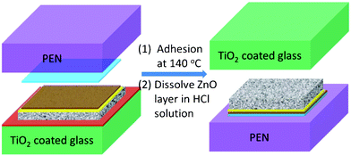 | ||
| Fig. 1 The process of integral transferring of TiO2 porous/TiO2 dense/FTO tri-layer from a glass substrate to a PEN substrate. The left part is the configuration before transfer, which includes (from bottom to top) TiO2 coated glass substrate (green), ZnO layer (red), TiO2 porous layer (white/black texture), TiO2 dense buffer layer (yellow), FTO layer (brown), hot-melt film (blue) and PEN substrate (purple). The right part is the configuration after transfer. | ||
To compare the transfer method with the conventional high temperature sintering method, we also fabricated devices on FTO glass substrates with the same device configuration without transfer. The active area of each device is 0.15 cm2 defined by a mask. Fig. 2 shows the J–V curves of devices with transferred TiO2 electrodes and high temperature sintered TiO2 electrodes. The transferred electrode with a TiO2 dense buffer layer has a light-to-electric power conversion efficiency (PCE) of 7.0% with a short circuit current density (Jsc) of 12.8 mA cm−2, an open circuit voltage (Voc) of 764 mV and a fill factor (FF) of 0.72. This performance is almost the same as that for non-transferred DSSCs fabricated with a high temperature process (PCE: 7.2%, Jsc: 12.9 mA cm−2, Voc: 775 mV, FF: 0.72), which indicates that the developed transfer method can be used to prepare high quality electrodes. On the other hand, the device efficiency without this TiO2 buffer layer was only 2.9% (Jsc: 10.4 mA cm−2, Voc: 574 mV, FF: 0.49), which indicates that the TiO2 dense buffer layer is an important component in this transfer method.
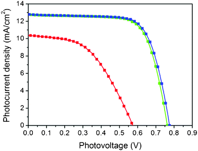 | ||
| Fig. 2 The photocurrent density–photovoltage curves of DSSCs with different TiO2 electrodes (blue line: non-transferred electrode with TiO2 dense buffer layer by high temperature sintering, green line: transferred electrode with TiO2 dense buffer layer, red line: transferred electrode without TiO2 dense buffer layer). | ||
Fig. 3a shows the cross-sectional morphology of FTO layer directly deposited on the TiO2 porous layers. The bottom TiO2 layer is highly porous and the top FTO layer is dense with well crystallized crystals. No clear boundary exists between the porous layer and the FTO layer, which indicates that an intermediate FTO layer with porous structure exists. The morphology of the initially deposited FTO in Fig. 3b shows that this intermediate layer is composed of small nanoparticles. For the FTO layer deposited on the TiO2 dense buffer layer (Fig. 3c), the intermediate layer is the TiO2 dense buffer layer. Fig. 3d shows that the initial deposition of FTO gives a well crystallized layer with almost no pores.
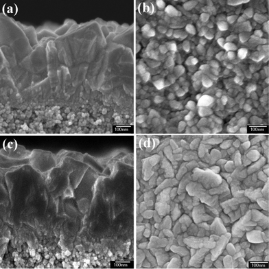 | ||
| Fig. 3 The cross-sectional SEM images of FTO layers deposition on TiO2 porous layer (a) and TiO2 dense buffer layer covered TiO2 porous layer (c). The surface morphologies of FTO layers prepared by spray pyrolysis of a small quantity of precursor solution (400 μL) on the TiO2 porous layer (b) and TiO2 dense buffer layer covered TiO2 porous layer (d). | ||
To understand the recombination process in the devices, we compared the impedance of transferred devices with and without TiO2 dense buffer layer at 0 V bias potential in Fig. 4. As the resistance of TiO2 at 0 V bias potential is very large, the impedance of the device mainly reflects the charge transfer at the FTO/electrolyte interface. The charge transfer resistance and interface capacitance can be deduced by fitting the impedance results with an equivalent circuit. The fitting results reveal that the charge transfer resistance and interface capacitance are 7.1 MΩ, 5.4 μF and 49.2 kΩ, 59.8 μF for the transferred devices with and without the TiO2 dense buffer layer, respectively. These data indicate that the dense buffer layer can remarkably increase the charge transfer resistance at FTO/electrolyte interface, which decreases the recombination occurrences. The large interface capacitance of devices without the dense buffer layer reflects that there is a large area of contact at FTO/electrolyte interface, which leads to low interface charge transfer resistance. The contact at FTO/electrolyte interface should be directly related to the FTO layer microstructure. For the FTO layer without dense buffer layer, the porous structure and the small particle size in the bottom part of the FTO layer would lead to the high contact area at the FTO/electrolyte interface.
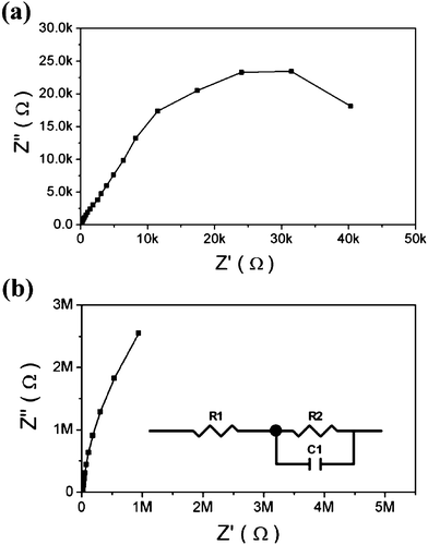 | ||
| Fig. 4 The dark impedance spectra (Nyquist plots) of DSSCs with different TiO2 electrodes at 0 V bias potential: (a) transferred electrode without TiO2 dense buffer layer, (b) transferred electrode with TiO2 dense buffer layer. | ||
Fig. 5 shows the impedance spectra of transferred DSSCs with and without the TiO2 dense buffer layer at −0.6 V bias potential. With the dense buffer layer, the impedance arch increases remarkably. As these impedances are measured at negative bias potentials, many electrons are present in the conduction band of the TiO2, which is similar to that under working conditions. The difference of impedance values indicates that the buffer layer can effectively block the recombination of DSSCs during its working condition. This is in agreement with the increased Jsc and Voc observed in the transferred DSSCs after using the buffer layer. As reported in previous studies, the impedance arch at high frequency in Fig. 5a comes from the large recombination at the FTO/electrolyte interface.10,11 This agrees with the impedance analysis at 0V bias potential.
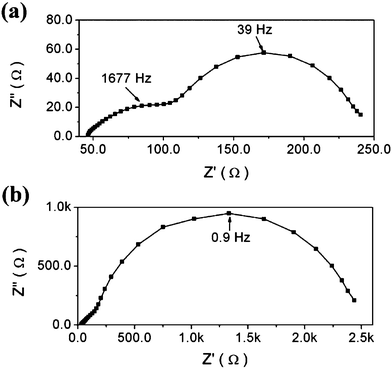 | ||
| Fig. 5 The dark impedance spectra (Nyquist plots) of DSSCs with different TiO2 electrodes at −0.6 V bias potential: (a) transferred electrode without TiO2 dense buffer layer, (b) transferred electrode with TiO2 dense buffer layer. | ||
Subsequently, the transfer technique was used to fabricate TiO2 porous electrodes on plastic substrates. As shown in Fig. 6, flexible DSSCs with the transferred TiO2 electrode on the bare PEN substrate (without ITO conductive layer) have a PCE of 6.4% with a Jsc of 11.9 mA cm−2, a Voc of 762 mV and a FF of 0.71. The Jsc of the transferred TiO2 electrode on PEN substrate is about 7% lower than that of the TiO2 electrode transferred on glass substrate. This is mainly due to the relatively lower transmittance of the PEN substrate.
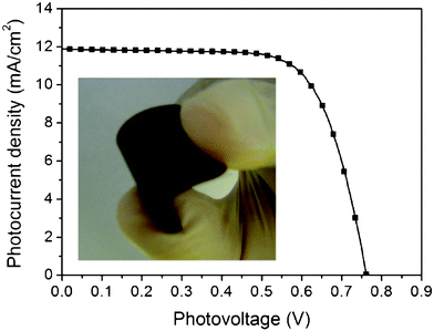 | ||
| Fig. 6 The photocurrent density–photovoltage curve of DSSC with the transferred TiO2 electrode on the PEN substrate. The inset image is the flexible D149 dye-sensitized TiO2 electrode. | ||
Conclusions
Efficient flexible TiO2 photoelectrodes were fabricated by transferring porous-TiO2/dense-TiO2/FTO tri-layers on PEN substrates. The similar light-to-electrical performances between transferred DSSCs and non-transferred DSSCs (high temperature prepared) indicates that the developed method can fabricate high quality photoelectrodes on plastic substrates. In this transfer method, a TiO2 dense buffer layer was added between the TiO2 porous layer and the FTO conductive layer, which improves the morphology of the deposited FTO layer and decreases the recombination at the FTO/electrolyte interface. By using this transfer method, an efficiency of 6.4% has been achieved for flexible DSSCs on PEN substrates under one sun condition.Acknowledgements
The authors are grateful to the National Research Foundation of Singapore (NRF-279-000-276-272), IMRE/11-1C0217 and the L’Oreal-Singapore Women for Science National Fellowship 2011 for financial support. Xizhe Liu is grateful to JiLin University for financial support (450091205331, 450091205348).References
- B. Oregan and M. Grätzel, Nature, 1991, 353, 737 CrossRef CAS.
- M. Nazeeruddin, A. Kay, I. Rodicio, R. Humphrybaker, E. Muller, P. Liska, N. Vlachopoulos and M. Grätzel, J. Am. Chem. Soc., 1993, 115, 6382 CrossRef CAS.
- Y. Lin, S. Wang, N. Fu, J. Zhang, X. Zhou and X. Xiao, Prog. Chem., 2011, 23, 548 CAS.
- (a) T. Yamaguchi, N. Tobe, D. Matsumoto and H. Arakawa, Chem. Commun., 2007, 4767 RSC; (b) H. Lindstrom, A. Holmberg, E. Magnusson, S. Lindquist, L. Malmqvist and A. Hagfeldt, Nano Lett., 2001, 1, 97 CrossRef; (c) S. Haque, E. Palomares, H. Upadhyaya, L. Otley, R. Potter, A. Holmes and J. Durrant, Chem. Commun., 2003, 3008 RSC; (d) H. Chen, C. Liang, H. Huang, J. Chen, R. Vittal, C. Lin, K. Wu and K. Ho, Chem. Commun., 2011, 47, 8346 RSC; (e) X. Yin, X. Liu, L. Wang and B. Liu, Electrochem. Commun., 2010, 12, 1241 CrossRef CAS.
- (a) D. Zhang, T. Yoshida and H. Minoura, Adv. Mater., 2003, 15, 814 CrossRef CAS; (b) D. Gutierrez-Tauste, I. Zumeta, E. Vigil, M. Hernandez-Fenollosa, X. Domenech and J. Ayllon, J. Photochem. Photobiol., A, 2005, 175, 165 CrossRef CAS.
- M. Durr, A. Schmid, M. Obermaier, S. Rosselli, A. Yasuda and G. Nelles, Nat. Mater., 2005, 4, 607 CrossRef.
- X. Huang, S. Huang, Q. Zhang, X. Guo, D. Li, Y. Luo, Q. Shen, T. Toyoda and Q. Meng, Chem. Commun., 2011, 47, 2664 RSC.
- L. Yang, L. Wu, M. Wu, G. Xin, H. Lin and T. Ma, Electrochem. Commun., 2010, 12, 1000 CrossRef CAS.
- (a) A. Burke, S. Ito, H. Snaith, U. Bach, J. Kwiatkowski and M. Grätzel, Nano Lett., 2008, 8, 977 CrossRef CAS; (b) S. Ito, P. Liska, P. Comte, R. Charvet, P. Péchy, U. Bach, L. Schmidt-Mende, S. Zakeeruddin, A. Kay, M. Nazeeruddin and M. Grätzel, Chem. Commun., 2005, 4351 RSC; (c) P. Cameron, L. Peter and S. Hore, J. Phys. Chem. B, 2005, 109, 930 CrossRef CAS.
- J. Bisquert, G. Garcia-Belmonte, F. Fabregat-Santiago and A. Compte, Electrochem. Commun., 1999, 1, 429 CrossRef CAS.
- J. Bisquert, Phys. Chem. Chem. Phys., 2000, 2, 4185 RSC.
| This journal is © The Royal Society of Chemistry 2012 |
