Transfer of asymmetric free-standing TiO2 nanowire films for high efficiency flexible dye-sensitized solar cells
Long
Wang
a,
Zhaosheng
Xue
ab,
Xizhe
Liu
a and
Bin
Liu
*ac
aDepartment of Chemical & Biomolecular Engineering, National University of Singapore, Singapore. E-mail: cheliub@nus.edu.sg
bNUS Graduate School for Integrative Sciences and Engineering (NGS), National University of Singapore, Singapore 117456
cInstitute of Materials Research and Engineering, 3 Research Link, Singapore 117602
First published on 14th June 2012
Abstract
A free-standing TiO2 nanowire thin film was prepared using the doctor-blade method. The film is composed of big and small nanowires on each side. The big nanowires have the functions of weakening adhesion to its original substrate, supporting the film after lift-off, and acting as a scattering layer in the final solar cells, whereas the small nanowires provide large surface area for dye loading and good adhesion to the flexible substrate for photoelectron collection. A high efficiency of 5.47% was obtained for flexible dye-sensitized solar cells fabricated by transferring the nanowire films onto ITO–PEN substrates.
Light-weight and flexible dye-sensitized solar cells (DSSCs) have attracted increasing attention in recent years because they are highly desirable as portable power supplies, and they can be manufactured via low cost and high productivity roll-to-roll mass production.1–4 However, good interconnection between TiO2 particles in DSSCs usually requires sintering process at temperatures that are much higher than the melting points of commonly used plastic flexible substrates. As a result, several “low temperature sintering” methods have been reported to develop flexible DSSCs on plastic substrates.2,4–7 However, the performances of these low-temperature sintered devices are generally not comparable to those with high-temperature sintering.8,9
An alternative strategy to fabricate flexible DSSCs is to transfer high-temperature sintered TiO2 films onto flexible substrates.9–13 So far, all the reported transfer methods require complex lifting-off processes and pretreatment on flexible substrates. Moreover, the lifted TiO2 films are fragile, which prevents their large-scale applications. On the other hand, recent studies on TiO2 nanowires (NWs) show that they could form free-standing films with ease and be synthesized at low cost.14,15
In this communication, we report a method to produce robust and free-standing asymmetric TiO2 NW films which can be automatically lifted off from its original substrate, and be readily attached to flexible substrates (Fig. 1). By transferring this asymmetric free-standing film onto an ITO-PEN substrate, we fabricated flexible DSSCs with 5.47% efficiency. The impedance analysis showed that the connection between transferred TiO2 and substrate is as good as high-temperature sintered ones even without any pretreatment on the secondary substrates.
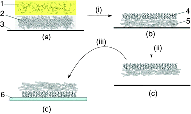 | ||
| Fig. 1 Illustration of the designed fabrication and transfer procedure using free-standing film method. (1) small nanowire paste; (2) big nanowire paste; (3) glass substrate; (4) small nanowire layer; (5) big nanowire layer; (6) flexible substrate. (i) High temperature treatment; (ii) cooling down to room temperature; (iii) transfer. (a) One layer of (2) and one layer of (1) formed on a piece of (3) using the doctor-blade method. (b) After (i), a free-standing film with layered structure was formed. (c) During (ii), the free-standing film automatically lifted off from (3). (d) The free-standing film was transferred onto a piece of (6) with small nanowires attached to substrate. | ||
The NWs were synthesized according to literature reports.14–16 The transmission electron microscopy (TEM) images of small and big NWs are shown in Fig. 2a and b, respectively. The lengths of the small NWs are ∼200 nm, and the diameters are ∼10 nm, while the big NWs are several micrometers long and ∼100 nm in diameter. The obtained NWs were converted to doctor-blade pastes,17 spread onto glass substrates with big NWs directly attached to the glass substrate and small NWs on the top, and then sintered at 550 °C for 30 min. Upon cooling down to room temperature, the film was automatically lifted off from glass substrate without any visible cracks. Fig. 2c shows a piece of free-standing flexible TiO2 film (inset picture) and its cross-sectional field emission scanning electron microscopy (FESEM) image. The film has a layered structure: the upper layer contains small NWs, while the bottom layer is composed of big NWs. From the cross-sectional image, the thicknesses are determined to be ∼6.5 μm and 5.5 μm for layers containing big and small NWs, respectively. The NW film was able to be automatically lifted off possibly due to at least three factors: 1) the big NWs are long enough to form a strong film, which is able to support itself and the upper small NW layer;14 2) as compared to small NWs or nanoparticles, the big NWs have weaker interaction with the substrate due to fewer connection points; 3) the thermal expansion coefficient of the TiO2 film is different from that of the glass substrate.
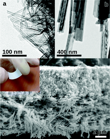 | ||
| Fig. 2 a and b: TEM image of as-synthesized small and big NWs. c: Cross-sectional FESEM image of a piece of free-standing flexible TiO2 nanowire film (inset figure), showing layered structure with small and big NWs on the top and bottom, respectively. | ||
To fabricate DSSCs using the free-standing film as the photoelectrode, two modifications were applied to the films in order to improve the device performance: 1) the films were treated with 80 mM TiCl4 aqueous solution at 70 °C for 30 min;16 and 2) Degussa P25 TiO2 nanoparticles were mixed with small NWs (wt% = 50%).18,19 A photoanode was fabricated by first attaching a piece of nanowire film to FTO-glass with the small NW side facing the substrate, then pressing the attached film for one minute at room temperature under a pressure of 0.6 t cm2, and finally immersing it into D149 dye solution for 2 h at room temperature. The dye solution contained 0.5 mM D149 and 0.5 mM chenodeoxycholic acid in acetonitrile and tert-butanol mixture (v/v 50/50). The DSSCs were assembled by clipping the photoanode and pyrolysis platinum electrode together, using a 25 μm hot melt film as the spacer. The electrolyte contained 0.6 M 1-butyl-3-methyl imidazolium iodide (BMII), 0.05 M I2, 0.1 M LiI and 0.05 M 4-tert-butylpyridine, in a mixture of valeronitrile and acetonitrile (v/v 15/85). The representative device was named as device A. The performance of device A is shown in Fig. 3. Device A has a light-to-electrical efficiency (η) of 6.24% with a short circuit photocurrent density (JSC) of 12.1 mA cm−2, an open circuit photovoltage (VOC) of 0.740 V and a fill-factor (FF) of 69.7%. The photocurrent–photovoltage (I–V) measurement was conducted under 100 mW cm−2 AM1.5 conditions, and a mask was used to keep the active area to be 0.158 cm2.
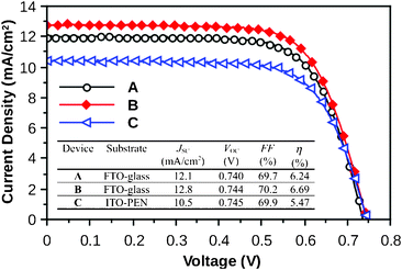 | ||
| Fig. 3 Performances of the devices. A: Transferred onto glass substrate. B: Non-transferred. C: Transferred onto flexible substrate. | ||
As a control, devices B were fabricated with exactly the same structure and film thicknesses as device A, but using the conventional method instead. A TiO2 film was prepared by spreading the NW pastes onto a FTO-glass substrate using the doctor-blade method with the big NWs on top of the small ones, which was followed by high-temperature sintering and TiCl4 treatment. All the other procedures were identical to those for device A. As shown in Fig. 3, these devices have an average η of 6.69%, a JSC of 12.8 mA cm−2, a VOC of 0.744 V and an FF of 70.2%. It is found that the energy conversion efficiency of a transferred device, A, is similar to the one fabricated with a standard method, B. This suggests that the qualities of the sintered TiO2 films are successfully retained by this transfer method. With the small NW attached to the glass substrate in device B, the film did not automatically lift off after sintering. In contrast, with the big NW attached to the glass substrate in device A, the film was not firmly adhered to the substrate after sintering. This suggests that the big NWs are the key for the TiO2 film to lift-off automatically after sintering.
Electrical impedance analysis was performed to understand the differences between devices A and B. The devices were measured in the dark with forward biases between 0.55 V and 0.75 V.20–22 The measured impedance spectra were then fitted with a transmission line model reported by Wang Q. et al.20. From the fitting results (Fig. 4), it is found that RCO (the resistance at TiO2/substrate interface) of a transferred device was only slightly higher than that of the non-transferred one (Avs.B: 2.56 Ω vs. 1.61 Ω at VOC). This finding is interesting, because the TiO2 film in device A is attached to the glass substrate by pressing while that in device B is directly sintered on the glass substrate. The strong adhesion formed between the film and substrate in device A by means of pressing alone is believed to be due to the NW film’s intrinsic flexibility and softness which aid in forming multiple strong connection points between itself and the glass substrate.
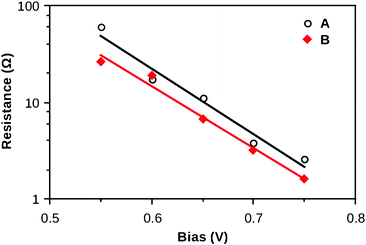 | ||
| Fig. 4 Fitted RCO v.s. bias voltage of devices transferred onto FTO-glass substrate (A) and control (B) obtained from the electrical impedance spectroscopy. | ||
We further investigated the working electrode by X-ray diffraction (XRD) and transmittance. Incident photo-to-electron conversion efficiency (IPCE) and I–V measurements were also used to understand the scattering effect of big NWs. It was reported that after sintering at 550 °C, the nanowires will crystallize with a mixture of anatase and rutile phases, whose particular composition depends highly on the sintering temperature and time.23 The XRD spectrum of the sintered NW film is shown in Fig. 5. Both anatase and rutile peaks can be found in the XRD pattern, thereby confirming that the NWs crystallized in a mixture of crystal phases. The transmittance spectra of the FTO substrate, small NW films with and without D149 are shown in Fig. 6a. In the short wavelength region, the transmittance of the NW film is lower than that of FTO-glass, which is due to the light absorption of TiO2 film as well as the slight light scattering in this region. In addition, D149 dye has two strong absorption peaks near 390 and 520 nm, which are in good agreement with the IPCE of devices without the big NW scattering layer. For devices with the big NW scattering layers, however, the IPCE in the wavelength ranges of 400–490 nm and 620–730 nm is enhanced because of the scattering effect of the big NWs. This is further confirmed by comparing the performances of devices with and without big NWs fabricated directly on FTO-glass substrate: their efficiencies are 5.90% vs. 6.69%, with JSC of 11.3 vs. 12.8 (mA cm−2), VOC of 0.745 vs. 0.744 (V), and FF of 70.1% vs. 70.2%.
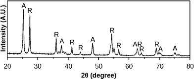 | ||
| Fig. 5 XRD patterns of NWs sintered at 550 °C for 30 min. A: Anatase peaks; R: rutile peaks. | ||
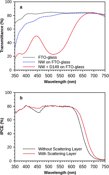 | ||
| Fig. 6 a: Transmittance (against air background) of small NW films with and without adsorbing D149 dye, as well as the FTO-glass substrate used in this work. b: IPCE of NW based devices with and without a big NW layer as scattering layer. | ||
Using the fabrication conditions on FTO-glass substrate, we further fabricated a flexible DSSC on ITO–PEN substrate, with the glass based counter electrode replaced by ITO–PEN with 100 nm platinum. As shown in Fig. 3, this device (device C) has an η of 5.47% with a JSC of 10.5 mA cm−2, a VOC of 0.745 V and a FF of 69.9%. Compared to device A, device C has a lower performance mainly due to the drop of photocurrent, which is in turn possibly caused by the stronger light absorption of the plastic substrate in device C as compared to the FTO-glass substrate used in device A.4
Conclusions
In this study, an asymmetric free-standing flexible TiO2 film was prepared using the simple doctor-blade method. Flexible DSSCs were fabricated by transferring the free-standing films onto ITO–PEN substrates, without any pretreatment on the substrate required. The energy conversion efficiency of the flexible DSSC is 5.47%. Electrical impedance analysis showed good connection between the transferred film and its substrate.Acknowledgements
The authors are grateful to the A-Star of Singapore (R-279-000-221-305), the Institute of Materials Research and Engineering (IMRE/11-1C0217), the National Research Foundation (R279-000-276-272) and the Lóreal-Singapore Women in Science National Fellowship 2011 for financial support.References
- X. Liu, Y. Luo, H. Li, Y. Fan, Z. Yu, Y. Lin, L. Chen and Q. Meng, Chem. Commun., 2007, 2847–2849 RSC.
- T. Yamaguchi, N. Tobe, D. Matsumoto and H. Arakawa, Chem. Commun., 2007, 4767–4769 RSC.
- D. Zhang, T. Yoshida, T. Oekermann, K. Furuta and H. Minoura, Adv. Funct. Mater., 2006, 16, 1228–1234 CrossRef CAS.
- X. Yin, X. Liu, L. Wang and B. Liu, Electrochem. Commun., 2010, 12, 1241–1244 CrossRef CAS.
- Y. Djaoued, S. Badilescu, P. V. Ashrit, D. Bersani, P. P. Lottici and R. Brüning, J. Sol-Gel Sci. Technol., 2002, 24, 247–254 CrossRef CAS.
- D. Zhang, T. Yoshida and H. Minoura, Adv. Mater., 2003, 15, 814–817 CrossRef CAS.
- F. Pichot, J. R. Pitts and B. A. Gregg, Langmuir, 2000, 16, 5626–5630 CrossRef CAS.
- S. Ito, N.-L. C. Ha, G. Rothenberger, P. Liska, P. Comte, S. M. Zakeeruddin, P. Péchy, M. K. Nazeeruddin and M. Grätzel, Chem. Commun., 2006, 4004–4006 RSC.
- M. Durr, A. Schmid, M. Obermaier, S. Rosselli, A. Yasuda and G. Nelles, Nat. Mater., 2005, 4, 607–611 CrossRef.
- L. Yang, L. Wu, M. Wu, G. Xin, H. Lin and T. Ma, Electrochem. Commun., 2010, 12, 1000–1003 CrossRef CAS.
- J. H. Park, T.-W. Lee and M. G. Kang, Chem. Commun., 2008, 2867–2869 RSC.
- A. Mihi, C. Zhang and P. V. Braun, Angew. Chem., Int. Ed., 2011, 50, 5712–5715 CrossRef CAS.
- X. Huang, S. Huang, Q. Zhang, X. Guo, D. Li, Y. Luo, Q. Shen, T. Toyoda and Q. Meng, Chem. Commun., 2011, 47, 2664–2666 RSC.
- X. Zhang, A. J. Du, P. Lee, D. D. Sun and J. O. Leckie, J. Membr. Sci., 2008, 313, 44–51 CrossRef CAS.
- J. Ng, X. Zhang, T. Zhang, J.-H. Pan, J.-H. A. Du, D. D. Sun and J. Chem, J. Chem. Technol. Biotechnol., 2010, 85, 1061–1066 CrossRef CAS.
- Y. Ohsaki, N. Masaki, T. Kitamura, Y. Wada, T. Okamoto, T. Sekino, K. Niihara and S. Yanagida, Phys. Chem. Chem. Phys., 2005, 7, 4157–4163 RSC.
- S. Ito, P. Chen, P. Comte, M. K. Nazeeruddin, P. Liska, P. Péchy and M. Grätzel, Progr. Photovolt.: Res. Appl., 2007, 15, 603–612 CrossRef CAS.
- B. Tan and Y. Wu, J. Phys. Chem. B, 2006, 110, 15932–15938 CrossRef CAS.
- Y. Xiao, J. Wu, G. Yue, G. Xie, J. Lin and M. Huang, Electrochim. Acta, 2010, 55, 4573–4578 CrossRef CAS.
- Q. Wang, S. Ito, M. Grätzel, F. Fabregat-Santiago, I. Mora-Seró, J. Bisquert, T. Bessho and H. Imai, J. Phys. Chem. B, 2006, 110, 25210–25221 CrossRef CAS.
- V. Yong, S.-T. Ho and R. P. H. Chang, Appl. Phys. Lett., 2008, 92, 143506 CrossRef.
- T. Hoshikawa, R. Kikuchi and K. Eguchi, J. Electroanal. Chem., 2006, 588, 59–67 CrossRef CAS.
- L. Zhang, H. Lin, N. Wang, C. Lin and J. Li, J. Alloys Compd., 2007, 431, 230–235 CrossRef CAS.
| This journal is © The Royal Society of Chemistry 2012 |
