Stoichiometry-controlled growth of BaxSr1−xTiO3 thin films and their electrical behavior in heterojunction assemblies†
Soumen
Das‡
a,
Daan
Liu‡
a,
Vallivedu
Janardhanam
b,
Chel-Jong
Choi
b and
Yoon-Bong
Hahn
*ab
aSchool of Semiconductor and Chemical Engineering, Chonbuk National University, 567 Baekjedaero, Deokjin-gu, Jeonju 561–756, Republic of Korea. E-mail: ybhahn@chonbuk.ac.kr; Fax: 82-63-270-2306.
bWCU Department of BIN Fusion Technology, Chonbuk National University, 567 Baekje-daero Deokjin-gu, Jeonju, 561-756, Republic of Korea
First published on 17th September 2012
Abstract
We describe an optimized chemical synthesis route to obtain BaxSr1−xTiO3 (x = 0, 0.50, 0.67, 1.0) thin films with impeccable stoichiometry control. The molar ratios of the precursors were altered to produce the cubic phase of SrTiO3, Ba0.5Sr0.5TiO3, Ba0.67Sr0.33TiO3 and the tetragonal phase of BaTiO3 thin films on single crystalline p-Si (100) and quartz substrates. The obtained Raman spectra for the BaxSr1−xTiO3 thin films on quartz substrates showed characteristic vibration modes at ∼303, 515 and 716 cm−1. The active modes of BaTiO3 signify the tetragonal phase, which is important for its various technological advantages. The significant features of these materials were obtained through capacitance–voltage (C–V) measurements with Pt (or Ag)/BaxSr1−xTiO3/p-Si/Pt (or Ag) assemblies, at 1, 10 and 100 kHz. Substantial hysteresis (ΔV) of 315 mV (with Ag) and 219 mV (with Pt) was observed for Ba0.5Sr0.5TiO3, whereas for BaTiO3 and SrTiO3 the obtained hysteresis was 256 mV and 96 mV, respectively. The largest hysteresis of 793 mV was observed for SrTiO3 with a Pt electrode. The above findings are important for assessing the device compatibility of cost efficient solution processed BaxSr1−xTiO3 thin films.
Introduction
Thin films of BaTiO3, SrTiO3, Ba0.50Sr0.50TiO3 and Ba0.67Sr0.33TiO3 are very interesting materials, due to their high dielectric, ferroelectric, piezoelectric and pyroelectric properties.1–5 These films have very high technological importance in microwave filters, resonators, read and write memory devices, charge storage and capacitors.6–11 It was reported that Ba0.60Sr0.40TiO3 thin films show high permittivity (∼428) and tenability (∼41%, at 300 kV cm−1 and 40 GHz), which make them suitable for the development of tunable high frequency microwave elements.12,13 Li et al.14 reported the synthesis of oleic acid capped barium strontium titanate (OA-BST) nanoparticles for solution-processed organic thin-film transistors (OTFTs). It was also shown that with increasing Ba2+ loading, along with the reduction of the Sr2+ contents in the compound, the dielectric constant drops. Yang et al.15 investigated the correlation of the band energetics of the nanostructured SrTiO3 electrode with the photoelectrochemistry of a cis-bis-(4,4′-dicarboxy-2,2′-bipyridine) dithiocyanato ruthenium(II) (Ru(dcbpy)2(NCS)2), N3-sensitized SrTiO3 electrode. The experimental results demonstrate that it is quite feasible to tune the band energetics of nanostructured SrTiO3 electrodes for dye-sensitized solar cells by optimization of electrolyte composition, in order to attain efficient photoelectric conversion. The non-volatile polarization of a ferroelectric is also a promising candidate for digital memory applications, and has been successfully integrated with silicon electronics.16,17 Moreover, as a nanogenerator on flexible substrates, or as a photocatalyst electrode for water splitting under visible-light irradiation, perovskite materials hold adequate importance in the contemporary research trend.18,19However, proper stoichiometric control of these materials is important for invoking the high dielectric constant in these materials. The qualitative assessment of these films is generally performed by concentrating on a number of issues, such as phase stability, doping mechanism, electronic structures,20,21 band alignment,22 and transport properties including carrier concentrations and conductivity. The issues with high dielectric or ferroelectric perovskite materials are that their dielectric constants (ε) decrease with decreasing physical thickness.23,24 Owing to their multi-cation composition, the optimum ε value is acquired only in a very narrow stoichiometric range. Thus, researchers pursue the object of optimizing the growth conditions for single phase high dielectric materials or finding effective doping to alter the electronic and lattice environment for better utilization of such materials. For instance, BaTiO3 exists in various crystallographic phases, such as tetragonal and cubic, and though the tetragonal phase is thermodynamically stable, most synthesis routes result in the cubic phase, which does not have much potential because it is paraelectric in nature.25,26 There have been reports on the wet chemical synthesis of cubic phase SrTiO3 and BaSrTiO3,27,28 but chemical synthesis of most tetragonal BaTiO3 took place through the hydro or solvothermal route.29,30 In all cases, no common synthesis route could be applicable to generate all the intended perovskite materials and thin film deposition with proper composition and desired permittivity was even more difficult. Since the electrical properties of ferroelectric thin films are strongly related to the microstructure and crystalline features of the materials, a small change in composition affects the physical states of the films processed under specified conditions. However, the advantage of solution processed thin films would be their cost effectiveness in obtaining larger areas of complicated geometries with accurate and reproductive control of the stoichiometry.
Here we present a report on an optimized inexpensive synthesis route to prepare homogeneous, crystalline BaxSr1−xTiO3 oxide films. Compared to the solid–solid reaction and the hydro or solvothermal processes, which obtain the desired perovskite phases with much effort and unconfirmed reproducibility, the advantage of the present synthesis route is that it facilitates a single approach with identical post-film-deposition annealing conditions to obtain phase pure samples with impeccable stoichiometric control. Unlike other chemical synthesis techniques which require carefully maintained carbon dioxide (CO2) free solvents to produce phase pure BaTiO3 in inert atmosphere, the present method categorically demonstrated a hassle free direct method to obtain the required phases. The synthesis route is distinctive, in the sense that no previous report has attempted to introduce identical and optimized synthesis parameters to realize phase pure BaxSr1−xTiO3 thin films on different substrates. The present method will aid in producing all-solution processed devices, which require high purity and close control over composition and microstructure.
Experimental section
Clean BaxSr1−xTiO3 (x = 0, 0.50, 0.67, 1.0) solutions were prepared with titanium butoxide (0.002 M) with acetylacetone and 2-ethoxyethanol. Ba-acetate (Ba(C2H3O2)2) or Sr-acetate (Sr(C2H3O2)2), or a mixture of these two (viz. Ba-acetate and Sr-acetate for BaxSr1−xTiO3, x = 0.50, 0.67) were dissolved in a mixture of acetic acid and deionized water (1.2![[thin space (1/6-em)]](https://www.rsc.org/images/entities/char_2009.gif) :
:![[thin space (1/6-em)]](https://www.rsc.org/images/entities/char_2009.gif) 1 v/v) in the desired molar percentage. The solution was heated at 85 °C for 15 min. The dissolved acetate precursor solutions were then mixed slowly with a titanium based solution under stirring. The solution was finally filtered with 0.1 μm filters. Thin films were spin-coated on the p-Si (100) and quartz substrates, either single or multiple (three, five and seven) times, to obtain the required film thickness. For such multiple coated samples, each intermediate coating was dried at 70 °C for 10 min (Case I) or at 350 °C for 10 min (Case II). The coated samples were finally annealed for 1 h at (a) 500 °C (b) 600 °C, (c) 700 °C and (d) 800 °C in an O2 atmosphere (100 sccm). We will see in the subsequent text that the intermediate drying process (refer to Case I and II) affects the final crystallographic phase and film thickness. The cross-section and thickness of the films deposited on the silicon substrates through Case II were measured by field emission scanning electron microscopy (FESEM, Hitachi JEOL 4800), and the topographic features were studied with an atomic force microscope (AFM, Nanoscope IV microscope controller). The crystallographic phases of the obtained BaxSr1−xTiO3 (x = 0, 0.5, 0.67 and 1) thin films, with a thickness of ∼130 nm, were investigated by grazing incidence X-ray diffractometer (XRD) with a Bruker axs (D8 advance) diffractometer supported by a LynXEye super-speed detector and Ni-filtered Cu-Kα (λ = 0.15406 nm) radiation generated at 45 kV/40 mA. The alignment was done to find the best parameters, such as the z-axis, ω, ϕ, etc by performing manual scanning for the appropriate sample position. The Raman spectra were obtained using the Renishaw Ramanscope system (2000 micro-Raman spectrometer) equipped with an optical microscope (Olympus BH2) and a He–Cd laser with excitation at 532 nm. The binding energies of the core level Ba, Sr, Ti and O were studied with X-ray photoelectron spectroscopy (XPS), recorded with a Thermo K-α ESCA system with a monochromatic Al-Kα source and a charge neutralizer. Capacitance–voltage (C–V) measurements of the BaxSr1−xTiO3 thin films deposited on the p-Si (100) were carried out with an LCR meter (Agilent 4284A). For C–V measurements, films obtained through Case II were chosen and Ag or Pt electrodes were deposited.
1 v/v) in the desired molar percentage. The solution was heated at 85 °C for 15 min. The dissolved acetate precursor solutions were then mixed slowly with a titanium based solution under stirring. The solution was finally filtered with 0.1 μm filters. Thin films were spin-coated on the p-Si (100) and quartz substrates, either single or multiple (three, five and seven) times, to obtain the required film thickness. For such multiple coated samples, each intermediate coating was dried at 70 °C for 10 min (Case I) or at 350 °C for 10 min (Case II). The coated samples were finally annealed for 1 h at (a) 500 °C (b) 600 °C, (c) 700 °C and (d) 800 °C in an O2 atmosphere (100 sccm). We will see in the subsequent text that the intermediate drying process (refer to Case I and II) affects the final crystallographic phase and film thickness. The cross-section and thickness of the films deposited on the silicon substrates through Case II were measured by field emission scanning electron microscopy (FESEM, Hitachi JEOL 4800), and the topographic features were studied with an atomic force microscope (AFM, Nanoscope IV microscope controller). The crystallographic phases of the obtained BaxSr1−xTiO3 (x = 0, 0.5, 0.67 and 1) thin films, with a thickness of ∼130 nm, were investigated by grazing incidence X-ray diffractometer (XRD) with a Bruker axs (D8 advance) diffractometer supported by a LynXEye super-speed detector and Ni-filtered Cu-Kα (λ = 0.15406 nm) radiation generated at 45 kV/40 mA. The alignment was done to find the best parameters, such as the z-axis, ω, ϕ, etc by performing manual scanning for the appropriate sample position. The Raman spectra were obtained using the Renishaw Ramanscope system (2000 micro-Raman spectrometer) equipped with an optical microscope (Olympus BH2) and a He–Cd laser with excitation at 532 nm. The binding energies of the core level Ba, Sr, Ti and O were studied with X-ray photoelectron spectroscopy (XPS), recorded with a Thermo K-α ESCA system with a monochromatic Al-Kα source and a charge neutralizer. Capacitance–voltage (C–V) measurements of the BaxSr1−xTiO3 thin films deposited on the p-Si (100) were carried out with an LCR meter (Agilent 4284A). For C–V measurements, films obtained through Case II were chosen and Ag or Pt electrodes were deposited.
Results and discussion
The XRD crystallographic phases of the deposited BaxSr1−xTiO3 (x = 0, 0.5, 0.67 and 1) thin films are represented in Fig. 1 (Case I, see experimental section). The cross section (thickness ∼130 nm) of a represented film is shown in Fig. 1S (ESI†). It is observed that no crystalline phase appears, as the samples are largely amorphous at 500 °C. At 600 °C, substantial crystalline features are observed for Ba0.67Sr0.33TiO3 and Ba0.50Sr0.50TiO3 thin films through high intensity XRD peaks, whereas no crystalline features were observed for SrTiO3 and BaTiO3 thin films at this temperature. Phase pure polycrystalline BaTiO3, Ba0.67Sr0.33TiO3, Ba0.50Sr0.50TiO3 and SrTiO3 thin films were obtained at 700 °C. The high intensity peaks of the films are identified as those from the tetragonal BaTiO3, cubic Ba0.67Sr0.33TiO3, Ba0.50Sr0.50TiO3 and SrTiO3 phases (Fig. 1c).31 The tetragonal phase of the BaTiO3 thin films is further confirmed through Raman spectroscopy, which is discussed in the next section. Fig. 1d shows that the BaTiO3 and SrTiO3 thin films annealed at 800 °C retain their respective phases, whereas a small impurity peak (marked by *) appears both for the cubic Ba0.67Sr0.33TiO3 and Ba0.50Sr0.50TiO3 films at this temperature.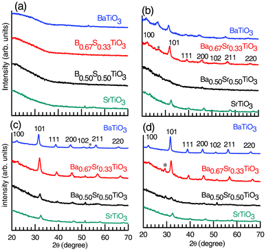 | ||
| Fig. 1 The XRD patterns for BaxSr1−xTiO3 (molar fraction, x = 0, 0.5, 0.67 and 1) thin films annealed at (a) 500, (b) 600, (c) 700 and (d) 800 °C for 1 h in an O2 atmosphere (100 sccm) (Case I, see experimental section). The phases are identified as desired perovskite phases; however, the impurity phase (marked by *) is also present in the crystalline samples. | ||
The XRD patterns in Fig. 2 present a different picture of phase evolution (for Case II, see experimental section) with respect to that described in Fig. 1. At 500 °C (a), the amorphous features are evident in all the film samples, whereas at 600 °C (b), except for BaTiO3, the other three samples (i.e. Ba0.67Sr0.33TiO3, Ba0.50Sr0.50TiO3 and SrTiO3) show high crystalline features. The BaTiO3 films, on the other hand, show an impurity phase (marked by *) at 2θ = 26.68°. A significant improvement in the crystallinity of all the samples over previous samples (Case I) is observed at 700 (c) and 800 °C (d). The peak intensities in all cases are appreciably high and no impurity phase is observed. The cross-sectional images of such films (Case II) with variable thickness for multiple coated samples are given as Fig. 2S (ESI†). As in Fig. 1, the tetragonal BaTiO3 and cubic Ba0.67Sr0.33TiO3, Ba0.50Sr0.50TiO3 and SrTiO3 phases are identified.31
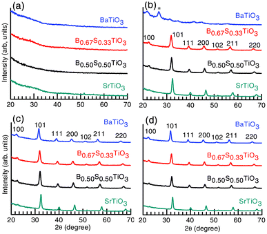 | ||
| Fig. 2 The XRD patterns for BaxSr1−xTiO3 (molar fraction, x = 0, 0.5, 0.67 and 1) thin films annealed at (a) 500, (b) 600, (c) 700 and (d) 800 °C for 1 h in an O2 atmosphere (100 sccm) (Case II, see experimental section). The desired perovskite phases with highly crystalline features are identified. | ||
It is assumed that the intermediate drying process triggers the preliminary growth kinetics in order to set the suitable thermodynamic energy for proper phase evolution. The diffusion and surface reaction play important roles in the grain growth process as well. It is a fact that the crystallographic evolution follows similar growth patterns for the films on quartz as well as on silicon (p-Si), leaving room to conclude that the orientation of the substrates and the ordering of the lattice have a minimal effect on the development of the crystal structures. In our study, the X-ray diffraction pattern revealed that the films dried at lower temperatures (85 °C) evolved with a higher percentage of impure phases after sintering than those films obtained after preliminary rapid drying at a much higher temperature (350 °C). This perhaps indicates that with the Ba2+ or Sr2+ diffusion through the short-cut path including the porous regime and grain boundaries, the critical drying temperature (in our case, 350 °C) initiates this migration of ions, which continues even during high temperature annealing. In this case, thermal energy promotes phase transformation according to the thermodynamic laws. Therefore, drying at a higher temperature might lead to a different transformation route to that observed at lower temperatures. In a report by Okubo et al.,32 the effect of drying at higher temperatures on the phase transformation from hexagonal to cubic, and the cubic to lamellar phases of mesoporous Si is discussed. However, it appears that understanding of the phase evolution of BaxSr1−xTiO3 films with time and temperature requires detailed consideration of thermodynamics, crystallographic, and nucleation-related conditions.
In Fig. 3, the slow scans of the high intensity (101) peaks of the BaxSr1−xTiO3 thin film are shown and the 2θ positions of the observed peak are compared with the JCPDS database.31 The shift in the 2θ peak position is in accordance with the database, implying highly stoichiometric BaxSr1−xTiO3 thin films obtained through the optimized wet chemical synthesis route. The grain diameter (D) of the individual films is calculated from Scherrer's equation33 to be DBTO ∼ 4.4 nm, DBSTO ∼ 9.2 nm and DSTO ∼ 10.4 nm, respectively. The topographic AFM images of these films with calculated surface roughness in root-mean-square (rms) are shown in Fig. 3S (ESI†). We observed differing roughness of the obtained samples, with STO registering the least roughness (∼1.10 nm), while BSTO has the largest roughness of all the samples at ∼1.78 nm.
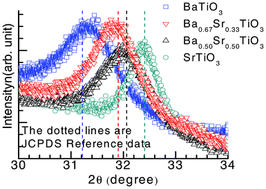 | ||
| Fig. 3 High-resolution XRD patterns of (101) peaks of tetragonal BaTiO3, and cubic Ba0.67Sr0.33TiO3, Ba0.50Sr0.50TiO3 and SrTiO3 thin films. The dotted vertical lines are the peak positions (2θ), in accordance with the JCPDS Database.31 | ||
An important identification process of the phases of BaxSr1−xTiO3 thin films involves room temperature Raman spectroscopy. Fig. 4a shows the room temperature Raman spectra for all the perovskite thin films deposited on quartz and annealed at 700 °C for 1 h in an O2 atmosphere (Case II). The frequency range is 100–800 cm−1. The Raman spectra from the unannealed and annealed quartz substrates are provided in Fig. 4S (ESI†) for recording the contribution of the substrate. The XRD patterns of these samples with characteristic peaks (as discussed in the sections related to Fig. 1 and 2 above) are also shown in Fig. 4b. Active Raman modes of tetragonal BaTiO3 (with C4v symmetry) are 4E(TO + LO) + 3A1(TO + LO) + B1(TO + LO), while no Raman-active mode is predicted for the cubic phase, which has Oh symmetry with a 3F1u + F2u optical branch and a F1u acoustical branch. The phonon symmetry for Raman active modes for the SrTiO3 crystal are interpreted as being primarily a first order Raman spectrum arising from deviations from the ideal cubic symmetry. These include four transverse T1u modes and one optically inactive T2u mode at the Γ(000) point of the Brillouin zone; one T1u mode is acoustic. Three phonon modes of the T1u symmetry are infrared (IR) active and one mode of the T2u symmetry is neither infrared nor Raman active. The latter mode is connected with the displacement of the O atom only.34–36 The cubic structure of BaxSr1−xTiO3 has five atoms per unit cell, and therefore, among 12 optical vibrational modes, the zone center optical phonons belong to the 3F1u + F2u modes. Each of the Fu modes is triply degenerate, and all of them are of odd parity with respect to inversion and therefore forbidden in first order Raman scattering. The F1u modes are infrared active, while the F2u modes are silent.37 For BaTiO3, the E(TO) modes with frequency 515 cm−1 come from the F1u cubic phase mode, which is also observed for the BaxSr1−xTiO3 (x = 0, 0.5, 0.67) thin films. The 303 cm−1 E mode comes from the cubic silent F2u mode. Interestingly, the Raman mode at 303 cm−1 is characteristic of tetragonal BaTiO3.38 The frequencies 637 and 716 cm−1 are the basis of the E(LO) modes. According to the literature survey,39 the phonon assignments for each of the active modes are: 716 cm−1(E(4LO) + A1(3LO)), 515 cm−1 (E(4TO) + A1(3TO)) and 303 cm−1 (E(3TO) + E(2LO) + B1). For SrTiO3 and BaxSr1−xTiO3, the most intense peak appeared at ∼517 cm−1. We have learnt from other reports that the three phonon modes of T1u symmetry appear at ∼90, 10 and 540 cm−1. 35,36,40 However, the origin of this active optical phonon mode at ∼517 cm−1 could not immediately be identified.
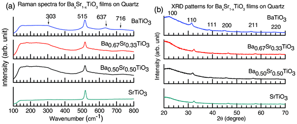 | ||
| Fig. 4 (a) The Raman spectra for BaxSr1−xTiO3 films deposited on quartz and annealed at 700 °C for 1 h in O2 (Case II). Characteristic active modes for perovskite BaxSr1−xTiO3 are observed at 313, 515, 637 and 716 cm−1, where the Raman mode at 303 cm−1 is characteristic of tetragonal BaTiO3. (b) The crystallographic phase of the studied respective BaxSr1−xTiO3 films deposited on quartz substrates. | ||
Fig. 5 shows the Ba3d, Sr3d, Ti2p and O1s peaks, with the spectra adjusted after alignment with a C1s binding energy of ∼285 eV. Table 1 presents the results of surface analysis of the BaTiO3, SrTiO3 and Ba0.50Sr0.50TiO3 films. The molar ratios of Ba/Ti, Sr/Ti and (Ba + Sr)/Ti are approximately unity. The probable difference in the chemical environments of the Ba, Sr and Ti molecules in three different films, viz. BaTiO3, SrTiO3 and Ba0.50Sr0.50TiO3, is observed in the obtained XPS spectra. For example, a shift of 0.50 eV is noted in the Sr2+![[thin space (1/6-em)]](https://www.rsc.org/images/entities/char_2009.gif) 3d core level peak of SrTiO3 and Ba0.50Sr0.50TiO3 (3rd column in Table 1). Similarly, a 0.68 eV shift is observed in the Ba2+
3d core level peak of SrTiO3 and Ba0.50Sr0.50TiO3 (3rd column in Table 1). Similarly, a 0.68 eV shift is observed in the Ba2+![[thin space (1/6-em)]](https://www.rsc.org/images/entities/char_2009.gif) 3d core level peak of BaTiO3 and Ba0.50Sr0.50TiO3 (4th column in Table 1). Interestingly, the Ti4+
3d core level peak of BaTiO3 and Ba0.50Sr0.50TiO3 (4th column in Table 1). Interestingly, the Ti4+![[thin space (1/6-em)]](https://www.rsc.org/images/entities/char_2009.gif) 2p peak position is identical (458.27 eV) in SrTiO3 and BaTiO3, although a shift of 0.32 eV is observed in case of Ti4+
2p peak position is identical (458.27 eV) in SrTiO3 and BaTiO3, although a shift of 0.32 eV is observed in case of Ti4+![[thin space (1/6-em)]](https://www.rsc.org/images/entities/char_2009.gif) 2p embedded in the cubic Ba0.50Sr0.50TiO3 lattice (5th column in Table 1, and see Fig. 5). However, the observed binding energy (BE) shift may also be due to the band alignment of the Ba0.50Sr0.50TiO3/Si interface.
2p embedded in the cubic Ba0.50Sr0.50TiO3 lattice (5th column in Table 1, and see Fig. 5). However, the observed binding energy (BE) shift may also be due to the band alignment of the Ba0.50Sr0.50TiO3/Si interface.
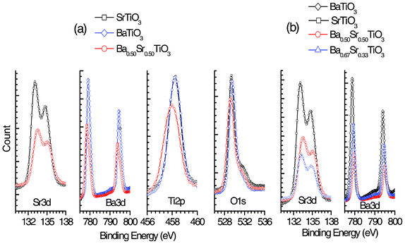 | ||
| Fig. 5 (a) and (b) show the core level binding energies of Sr3d, Ba3d, Ti2p and O1s of perovskite BaxSr1−xTiO3 (x = 0, 0.5, 0.67 and 1.0) thin films on silicon substrates obtained through Case II. The spectra are adjusted with a C1s peak position at 285 eV. The observed substantial shift in all other peak positions signifies chemical interactions among different parent molecules, as in the text we showed an insignificant band alignment. | ||
| O | Sr | Ba | Ti | |
|---|---|---|---|---|
| BaTiO3 (at%) | 57.02% | — | 21.18% | 17.87% |
| (peak position) | 529.56 eV | — | 779.18 eV | 458.27 eV |
| SrTiO3 (at%) | 54.01% | 14.81% | — | 15.56% |
| (peak position) | 529.4 eV | 133.09 eV | — | 458.27 eV |
| Ba0.50Sr0.50TiO3 (at%) | 55.98% | 9.65% | 12.03% | 17.01% |
| (peak position) | 529.30 eV | 133.59 eV | 778.5 eV | 457.95 eV |
| Ba0.67Sr0.33TiO3 (at%) | 55.25% | 11.62% | 14.62% | 17.67% |
| (peak position) | 532.88 | 133.42 | 779.35 | 457.65 |
The BE of the core level peaks and of the valence band are measured with reference to the Fermi level (EF). Therefore any change in the positions of the oxide energy levels and band edges relative to (EF) will result in a BE shift. In order to get an idea of BE shift due to band offset, we calculate the valence band offset of experimental Ba0.5Sr0.5TiO3 films deposited on p-Si (100). The valence band maximum for Ba0.50Sr0.50TiO3 is calculated as 2.23 eV and that of p-Si is calculated as 0.53 eV, obtained by using a linear extrapolation method suggested by McKee et al.41 The valence band offset (ΔEV) is calculated by the expression
| ΔEV = (2p-VBM)Ox – (2p-VBM)Si + ΔECL | (1) |
| ΔEb ≅ Δ(Va + Vea) − ΔRea | (2) |
Fig. 6 shows the capacitance–voltage (C–V) measurements of the Ag/BaxSr1−xTiO3/Si(100)/Ag (a) and Pt/BaxSr1−xTiO3/Si(100)/Pt (b) heterojunction assemblies at different frequencies, viz. at 1 kHz, 10 kHz and 100 kHz. All C–V measurements were carried out as cycle sweeps (+ve to –ve and in reverse) in order to check any possible hysteresis behavior. Fig. 6a represents the response of such an assembly for x = 1, 0.67, 0.5 and 0 with distinct accumulation, depletion and inversion regions. The C–V response from Ag/p-Si (100)/Ag is given in Fig. 5S (ESI†). The observed hysteresis (Fig. 6a) was a maximum in the case of Ba0.5Sr0.5TiO3 for all frequencies and a minimum for SrTiO3. Substantial hysteresis (ΔV) of ∼315 mV is observed for Ba0.5Sr0.5TiO3, whereas for BaTiO3 and SrTiO3 the obtained hysteresis is 256 and 96 mV, respectively, at a frequency of 10 kHz for the Ag electrode. For the Pt electrode, the observed ΔV (Fig. 6b) is a maximum in the case of SrTiO3 (793 mV) for all frequencies and a minimum for Ba0.5Sr0.5TiO3 (219 mV). The presence of hysteretic behavior indicated some degree of field-reversible in-plane polarization. The variation in the dielectric response with the dc electric field is associated with the domain reorientation process. Another possible reason is the charge trapped near the oxide–semiconductor interface. Given the oxide capacitance (Cox), when the assembly is biased for strong accumulation at high frequency, the magnitude of the charge trapped can be estimated as Qt = ΔVCox.43 For Ba0.5Sr0.5TiO3, Cox is 2.79 × 10⁻⁹ F, giving a total trapped charge of 8.78 × 10⁻¹⁰ C. Similarly, for BaTiO3 and SrTiO3, the values of Qt are 6.16 × 10⁻¹⁰ C and 5.07 × 10⁻¹⁰ C, respectively. The carrier density (N) can thus be calculated from Qt = qNd where d is the width of the depletion region. N is found from the slope of the 1/C2versus voltage (V) curve, while the intersection determines the built-in voltage. The reasonable fit at voltages close to zero signifies a uniform charge carrier concentration of ∼6.6 × 1019 cm−3 at the interface for Ba0.5Sr0.5TiO3/p-Si assembly. For the BaTiO3/p-Si and SrTiO3/p-Si interface, N ∼ 2.7 × 1019 cm−3 and 2.6 × 1019 cm−3, respectively. The differences in the capacitance values at negative and positive bias voltages can be ascribed to the formation of accumulation and depletion layers. The formation of such layers is originally due to the ferroelectric domain switching, which is responsible for the carrier accumulation in the film.22,44 The observed relatively large hysteresis for the Pt/SrTiO3/p-Si combination is ascribed to the effects of trap charges at the interface or effects resulting in polarization of the oxide thin films. Given that the trapped charge (Qt ∼ 1.41 × 10⁻¹⁰ C) for SrTiO3 in this case is four times smaller than in the case of Ag/SrTiO3/p-Si, the role of the electrode/oxide/semiconductor interfaces would remain a key factor to determine the shape of the hysteresis and the mechanism for charge trapping, mobility and injection.
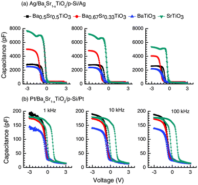 | ||
| Fig. 6 The capacitance (C)–voltage (V) responses of (a) Ag/BaxSr1−xTiO3/Si(100)/Ag and (b) Pt/BaxSr1−xTiO3/Si(100)/Pt at 1, 10 and 100 KHz. The BaxSr1−xTiO3 plots show the influence of the metal–pervoskite oxide thin film interface in determining the hysteresis (ΔV) and other related parameters, such as trap charges. | ||
Conclusions and summary
In summary, the present study highlighted the behavioral features of BaTiO3, Ba0.50Sr0.50TiO3, Ba0.67Sr0.67TiO3 and SrTiO3 films obtained through an optimized wet chemical synthesis route. The crystalline features and the evolution of the phase of the perovskite oxide materials are also discussed. The advantage of the present synthesis route was that it facilitated a single approach with identical post-film-deposition annealing conditions to obtain phase pure samples with impeccable stoichiometric control. The binding energy shift of the core level peak of Ba3d and Sr3d in the photoelectron spectroscopy was evaluated in terms of the local and chemical environment of the atoms in the lattice. The C–V characteristics were used to extract the concentration of free carriers in the depletion regime and to gather information on the influence of perovskite oxide/metal interfaces. These findings would assist in pursuing suitable cost effective microelectronic devices.Acknowledgements
This work was supported in part by the National Leading Research Lab. program (2012-0008816) and by the World Class University program (R31-20029) funded by the Korean government (MEST). Authors also thank KBSI, Jeonju branch for taking quality SEM images.References
- G. Houzet, K. Blary, S. Lepilliet, D. Lippens, L. Burgnies, G. Vélu, J. C. Carru, E. Nguéma and P. Mounaix, J. Appl. Phys., 2011, 109, 014116 CrossRef.
- S. Nazir and U. Schwingenschlögl, Appl. Phys. Lett., 2011, 99, 073102 CrossRef.
- U. Ellerkmann, R. Liedtke, U. Boettger and R. Waser, Appl. Phys. Lett., 2004, 85, 4708 CrossRef CAS.
- X. Hu, H. Li, Y. Liang, Y. Wei, Z. Yu, D. Marshall, Jr, J. Edwards, R. Droopad, X. Zhang, A. A. Demkov, K. Moore and J. Kulik, Appl. Phys. Lett., 2003, 82, 203 CrossRef CAS.
- X. Zhu, W. Peng, J. Miao and D. Zheng, Mater. Lett., 2004, 58, 2045–2048 CrossRef CAS.
- S. Gevorgian, Ferroelectrics in Microwave Devices, Circuits and Systems, Springer-Verlag London Limited, 2009 Search PubMed.
- W. Y. Fu, Z. Xu, L. Liu, X. D. Bai and E. G. Wang, Nanotechnology, 2009, 20, 475305 CrossRef CAS.
- G. N. Saddik, D. S. Boesch, S. Stemmer and R. A. York, Appl. Phys. Lett., 2007, 91, 043501 CrossRef.
- A. T. Findikoglu, Q. X. Jia, I. H. Campbell, X. D. Wu, D. Reagor, C. B. Mombourquette and D. McMurry, Appl. Phys. Lett., 1995, 66, 3674 CrossRef CAS.
- X. Y. Fang, O. K. Tan, Q. Wei, M. W. Yao and S. C. Tjin, Sens. Actuators, B, 2006, 119, 78–83 CrossRef.
- M. Izuha, K. Abe, M. Koike, S. Takeno and N. Fukushima, Appl. Phys. Lett., 1997, 70, 1405 CrossRef CAS.
- L. Yang, F. Ponchel, G. Wang, D. Rémiens, J. F. Légier, D. Chateigner and X. Dong, Appl. Phys. Lett., 2010, 97, 162909 CrossRef.
- M. Liu, C. Ma, G. Collins, J. Liu, C. Chen, L. Shui, H. Wang, C. Dai, Y. Lin, J. He, J. Jiang, E. I. Meletis and Q. Zhang, Cryst. Growth Des., 2010, 10, 4221–4223 CAS.
- Y. Gan, Q. J. Cai, C. M. Li, H. B. Yang, Z. S. Lu, C. Gong and M. B. Chan-Park, ACS Appl. Mater. Interfaces, 2009, 1, 2230–2236 CAS.
- S. Yang, H. Kou, J. Wang, H. Xue and H. J. Han, J. Phys. Chem. C, 2010, 114, 4245–4249 CAS.
- J. Hoffman, X. Pan, J. W. Reiner, F. J. Walker, J. P. Han, C. H. Ahn and T. P. Ma, Adv. Mater., 2010, 22, 2957–2961 CrossRef CAS.
- Z. Yan, Y. Guo, G. Zhang and J. M. Liu, Adv. Mater., 2011, 23, 1351–1355 CrossRef CAS.
- K. I. Park, S. Xu, Y. Liu, G. T. Hwang, S. J. L. Kang, Z. L. Wang and K. J. Lee, Nano Lett., 2010, 10, 4939–4943 CrossRef CAS.
- K. Iwashina and A. Kudo, J. Am. Chem. Soc., 2011, 133, 13272–13275 CrossRef CAS.
- S. Carter, A. Selcuk, R. J. Chater, J. Kajda, J. A. Kilner and B. C. H. Steele, Solid State Ionics, 1992, 53–56, 597–605 CrossRef CAS.
- D. N. Mueller, R. A. De Souza, H. I. Yoo and M. Martin, Chem. Mater., 2012, 24, 269–274 CrossRef CAS.
- S. Das, J. H. Kim, Y. K. Park and Y. B. Hahn, Appl. Phys. Lett., 2011, 98, 202102 CrossRef.
- H. Schroeder and S. Schmitz, Appl. Phys. Lett., 2003, 83, 4381 CrossRef CAS.
- C. B. Parker, J. P. Maria and A. I. Kingon, Appl. Phys. Lett., 2002, 81, 340 CrossRef CAS.
- M. Pasściak, S. E. Boulfelfel and S. Leoni, J. Phys. Chem. B, 2010, 114, 16465–16470 CrossRef.
- M. B. Smith, K. Page, T. Siegrist, L. P. Redmond, E. C. Walter, R. Seshadri, L. E. Brus and M. L. Steigerwald, J. Am. Chem. Soc., 2008, 130, 6955–6963 CrossRef CAS.
- A. F. Demirörs and A. Imhof, Chem. Mater., 2009, 21, 3002–3007 CrossRef.
- P. Vitanov, A. Harizanova, T. Ivanova, D. Velkov and Z. Raytcheva, Vacuum, 2003, 69, 371–377 CrossRef.
- Y. Wang, H. Xu, X. Wang, X. Zhang, H. Jia, L. Zhang and J. Qiu, J. Phys. Chem. B, 2006, 110, 13835–13840 CrossRef CAS.
- J. Y. Choi, C. H. Kim and D. K. Kim, J. Am. Ceram. Soc., 1998, 81, 1353–1356 CrossRef CAS.
- International Centre for Diffraction Data (1997 JCPDS), File No. 34-0129, 39-1395 and 35-0734.
- M. Ogura, H. Miyoshi, S. P. Naik and T. Okubo, J. Am. Chem. Soc., 2004, 126, 10937–109644 CrossRef CAS.
- A. L. Patterson, Phys. Rev., 1939, 56, 978–982 CrossRef CAS.
- A. Cracknell, B. Davies, S. Miller and V. Love, Kronecker Product Tables I: General Introduction and Tables of Irreducible Representations of Space Groups, IFI/Plenum, New York, Washington, London, 1979 Search PubMed.
- C. H. Perry, B. Khann and G. Rupprecht, Phys. Rev., 1964, 135, A408 CrossRef.
- S. Gupta and R. S. Katiyar, J. Raman Spectrosc., 2001, 32, 885–891 CrossRef CAS.
- D. A. Tenne and X. Xi, J. Am. Ceram. Soc., 2008, 91, 1820–1834 CrossRef CAS.
- Z. Lazarević, N. Romćević, M. Vijatović, N. Paunović, M. Romćević, B. Stojanović and Z. D. Mitrović, Acta Physica Polonica A, 2009, 115, 808–810 Search PubMed.
- J. Q. Qi, T. Peng, Y. M. Hu, L. Sun, Y. Wang, W. P. Chen, L. T. Li, C. W. Nan and H. L. W. Chan, Nanoscale Res. Lett., 2011, 6, 466 CrossRef.
- J. Han, F. Wan, Z. Zhu and W. Zhang, Appl. Phys. Lett., 2007, 90, 031104 CrossRef.
- R. A. McKee, F. J. Walker, M. B. Nardelli, W. A. Shelton and G. M. Stocks, Science, 2003, 300, 1726–1730 CrossRef CAS.
- W. F. Egelhoff, Surf. Sci. Rep., 1987, 6, 253–415 CrossRef.
- C. J. Park, K. H. Cho, W. C. Yang, H. Y. Cho, S. H. Choi, R. G. Elliman, J. H. Han and C. Kim, Appl. Phys. Lett., 2006, 88, 071916 CrossRef.
- Y. Feng, X. Wei, D. Wang, Z. Xu and X. Yao, Ceram. Int., 2004, 30, 1389–1392 CrossRef CAS.
Footnotes |
| † Electronic Supplementary Information (ESI) available. See DOI: 10.1039/c2ra20858j |
| ‡ These authors contributed equally to this article. |
| This journal is © The Royal Society of Chemistry 2012 |
