Facile microwave-assisted synthesis of uniform single-crystal copper nanowires with excellent electrical conductivity†
Yong-Qiang
Liu
ab,
Meng
Zhang
a,
Feng-Xia
Wang
a and
Ge-Bo
Pan
*a
aSuzhou Institute of Nano-tech and Nano-bionics, Chinese Academy of Sciences, Suzhou, 215123, P. R. China. E-mail: gbpan2008@sinano.ac.cn.; Fax: 86-512-62872663; Tel: 86-512-62872663
bGraduate University, Chinese Academy of Sciences, Suzhou, 215123, P. R. China
First published on 15th October 2012
Abstract
A facile and rapid route for the synthesis of uniform single-crystal copper nanowires by a microwave-assisted method is demonstrated. The as-prepared copper nanowires exhibit excellent conductivity, which is comparable with electrospun copper nanofibers.
Metal nanowires have attracted considerable attention because of their excellent electronic and optical properties. They have been used in many fields, such as displays, solar cells, touch-screens, sensors, and electromagnetic interference shielding.1 However, for most of these applications, metal nanowires with high electrical conductance are required. Compared with various other metals, copper is more abundant and less expensive, while having favourable mechanical, electrical, and optical properties.2 Copper nanowires (Cu NWs) have thus been suggested as a low-cost alternative to indium tin oxide (ITO), investigated extensively, and compared against conductive polymers, carbon nanotubes, graphenes, and Ag nanowires.3–6
To date, various methods have been developed for synthesizing Cu NWs, including electrochemical deposition, electrospinning, template processes, hydrothermal reduction, and reverse micellar systems.5–12 For instance, Rathmell et al. have synthesized Cu NWs in aqueous solution and evaluated their potential application in flexible and transparent conducting films. A sheet resistance of 30 Ω sq−1 at a transmittance of 85% was obtained.5 Wu et al. have fabricated transparent electrodes with electrospun Cu nanofibers, which displayed a sheet resistance of 50 Ω sq−1 at a transmittance of 90%.6 The above methods are generally complicated and time-consuming, although Cu NWs with controlled morphology and dimensions can be prepared. It remains a challenge to develop a facile and more effective method for the preparation of uniform single-crystal Cu NWs.
Herein, we report a facile and rapid route for the synthesis of uniform single-crystal Cu NWs by a microwave-assisted method. The Cu NWs were investigated by scanning electron microscopy (SEM), selected area electron diffraction (SAED), transmission electron microscopy (TEM), and X-ray diffraction (XRD). The effects of the amount of hexadecylamine (HDA), the molar ratio of ascorbic acid/CuCl2, and the reaction temperature and time on the growth of Cu NWs were elucidated. Moreover, the electrical conductance of the as-prepared Cu NWs was measured and exhibited excellent performance, which was comparable to electrospun copper nanofibers.
All the synthesis was performed in a microwave system (2.45 GHz, 300 W, Discover S-Class, CEM). In a standard synthesis, 8.4 mg anhydrous CuCl2, 11.1 mg ascorbic acid, 90 mg HDA, and 5 mL deionized water were mixed in a microwave vial and sealed with a Teflon cap. The final suspension was magnetically stirred at room temperature overnight. The vial was transferred into the microwave reactor and heated at 120 °C for 2 h. During the microwave irradiation, the suspension was stirred with a stir bar at high speed. When the reaction was completed, the suspension changed color from pale-yellow to red-brown, implying the formation of Cu NWs. This is due to the reduction of Cu2+ by ascorbic acid. The redox reaction can be expressed as:

The resulting reddish brown suspension was centrifuged and washed sequentially with deionized water (60 °C), n-hexane, and ethanol. For subsequent characterization, the reddish fluffy solid was dispersed in ethanol and drop-casted on different substrates.
Fig. 1a shows a typical SEM image of the as-prepared Cu NWs. It indicates that the Cu NWs could be prepared in high purity with simple post-synthesis separation. This result is similar to the literature.12 Note that in the present work, a very small amount of Cu nanoparticles is present. Nevertheless, such a small quantity of Cu nanoparticles could be removed by cross-flow filtration.13 The SEM image at a higher magnification (Fig. 1b) and TEM image (Fig. 1c) clearly reveal that the Cu NWs are uniform in diameter and tend to form some parallel bundles. The Cu NWs have an average diameter of 50 ± 10 nm (Fig. S1, ESI†) and lengths longer than 10 μm, i.e., an aspect ratio of greater than 300. In addition, the Cu NWs are highly flexible and some of them show bending. Fig. 1d shows a high-resolution TEM image of a single Cu NW. It is clear that the Cu NW is a single crystal with high lattice perfection. The fringes have lattice spacings of 2.12, 2.58 and 1.85 Å, which correspond to the {111}, {110} and {200} plane, respectively. The angle value between the {110} and {200} plane is close to the theoretical value. The growth direction of Cu NWs was along the 〈1ī0〉, which is also confirmed by the SAED image (inset in Fig. 1d).
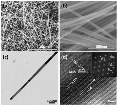 | ||
| Fig. 1 Structural and morphological characterization of Cu nanowires: (a) SEM image; (b) magnified SEM image; (c) TEM image; and (d) high-resolution TEM image. The inset in (d) shows an SAED image of single Cu nanowire in (c). | ||
Fig. 2a shows an XRD pattern of Cu NWs. The four peaks at 2θ = 43.5, 50.6, 74.3, and 90.2° correspond to the diffraction from {111}, {200}, {220}, and {311} planes of face-centered cubic Cu (JCPDS #03-1018), respectively. No other phases such as Cu2O and CuO are detected, indicating that pure metallic copper is obtained. Moreover, the oxidation of Cu NWs occurs relatively slowly at ambient conditions. Only a negligible peak of the phase of Cu2O is observed in the XRD pattern (Fig. S2, ESI†) after 30 days. Fig. 2b shows the UV-visible adsorption spectrum of Cu NWs dispersed in ethanol. A distinct peak could be observed at λ = 592 nm. This peak indicates the optical signatures of Cu NWs, and is attributed to the plasma excitation in Cu NWs.14 A similar absorption peak is also observed for Cu NWs synthesized by other methods.9,15
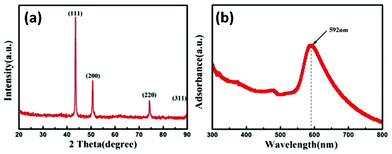 | ||
| Fig. 2 (a) XRD pattern of Cu nanowires prepared by the standard process. (b) UV-visible absorption spectrum of Cu nanowires dispersed in ethanol. | ||
Similarly to ethylenediamine,5 the addition of HDA to the reaction solution is necessary to promote anisotropic growth of Cu NWs. When HDA is not added to the reaction, only irregular particles with diameters ranging from 50–100 nm are obtained (Fig. 3a). The SAED pattern (Fig. S3, ESI†) indicates that the nanoparticles are polycrystalline. To explore the role of HDA as a capping agent, the effect of the amount of HDA on the growth of Cu NWs is investigated. Standard synthesis procedure was performed while varying the amount of HDA and keeping all other synthesis parameters fixed. When the amount of HDA added is 60 mg, only a small number of nanowires show up with many nanoparticles (Fig. 3b). This is reasonable, because only a few of the copper seeds have been effectively capped due to an insufficient HDA amount. Upon increasing the amount of HDA to 90 mg, nanowires are grown almost exclusively (Fig. 3c). This indicates that the facets of most copper seeds have been adhered selectively and effectively by HDA. As a result, preferential growth along the wire direction occurs. When the amount of HDA is 120 mg, a blended structure of nanoparticles and nanowires is obtained (Fig. 3d). This is because a large amount of HDA may cause high capping of wire ends as well as the sides. A similar result has been reported for the preparation of Ag nanowires, in which a relatively high amount of the capping agent of poly(vinylpyrrolidone) had led to an isotropic growth mode.16
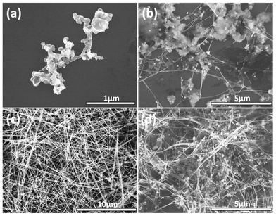 | ||
| Fig. 3 SEM image of Cu nanowires prepared by varying the amount of HDA while keeping all other synthesis parameters fixed. Samples (a), (b), (c) and (d) correspond to 0, 60, 90 and 120 mg, respectively. | ||
The molar ratio of ascorbic acid![[thin space (1/6-em)]](https://www.rsc.org/images/entities/char_2009.gif) :CuCl2 also plays an important role in the morphology and aspect ratio of Cu NWs, as has been revealed by SEM (Fig. S4, ESI†). At a molar ratio of ascorbic acid:CuCl2 of 1:2, Cu NWs are obtained as well as a small number of nanoparticles. The Cu NWs have an average diameter of ∼25 nm and an average length of more than 10 μm. Upon increasing the molar ratio of ascorbic acid/CuCl2 to 2:1, more and more nanoparticles are formed. The diameters of Cu NWs increase to ∼65 nm, while the lengths reduce to ∼4 μm. At a molar ratio of ascorbic acid:CuCl2 of 4:1, the product consists almost exclusively of nanoparticles and nanorods. The above results demonstrate the effective modulation of the molar ratio of ascorbic acid:CuCl2 on the morphology of final product. This is attributed to different redox reaction rates under different reaction conditions. In addition, a previous study also indicates that highly anisotropic structures tend to become favorable in a slow reduction process.17 A similar phenomenon has been reported in the literature.18
:CuCl2 also plays an important role in the morphology and aspect ratio of Cu NWs, as has been revealed by SEM (Fig. S4, ESI†). At a molar ratio of ascorbic acid:CuCl2 of 1:2, Cu NWs are obtained as well as a small number of nanoparticles. The Cu NWs have an average diameter of ∼25 nm and an average length of more than 10 μm. Upon increasing the molar ratio of ascorbic acid/CuCl2 to 2:1, more and more nanoparticles are formed. The diameters of Cu NWs increase to ∼65 nm, while the lengths reduce to ∼4 μm. At a molar ratio of ascorbic acid:CuCl2 of 4:1, the product consists almost exclusively of nanoparticles and nanorods. The above results demonstrate the effective modulation of the molar ratio of ascorbic acid:CuCl2 on the morphology of final product. This is attributed to different redox reaction rates under different reaction conditions. In addition, a previous study also indicates that highly anisotropic structures tend to become favorable in a slow reduction process.17 A similar phenomenon has been reported in the literature.18
The influence of temperature and time on the growth of copper nanowires was also investigated. The results indicate that a lower or higher reaction temperature (40 or 180 °C) did not lead to the growth of uniform copper nanowires, which is likely illustrated by reaction kinetics. The lower temperature could not active the specific facets for the anisotropic growth of nanowires. In contrast, the higher temperature may cause nanowire super-heating and further make them fuse into microscale clusters.16,17 The existence of copper clusters in the products prepared after 4–8 h microwave exposure supports nanowire super-heating in the synthesis process.
Compared to other metal NWs, Cu NWs can be prepared at lower cost while preserving favorable conductivity. As such, Cu NWs are expected to be a promising alternative to the commercial ITO, which is used for transparent electrodes and interconnects in optoelectronic devices. In order to perform the electrical measurements, Cu NWs were dispersed in ethanol, sonicated, and drop-casted on vacuum-deposited Au/Ti electrodes. The Au contacts are interdigital and have a width of 20 μm and spacing of 20 μm. Fig. 4a shows a schematic diagram of NWs resting across the interdigital gold electrodes. Fig. 4b shows a typical I–V curve of Cu NWs film recorded with the two-probe method. It is clear that the current is linear and independent of the gate voltage. This indicates the intrinsic metal nature. At a fixed voltage of 100 mV, the maximum electric current of Cu NWs film could be close to 1 mA. This value is comparable to an electrospun copper nanofiber network.6 However, it is important to point out that all the electrical measurements in the present study were performed at ambient conditions.
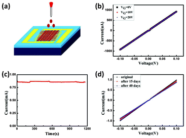 | ||
| Fig. 4 (a) Schematic diagram of the device for electrical measurement. (b) I–V curves of Cu nanowire film with different gate voltages. (c) I–t curve recorded continuously over 1200 s at ambient conditions. The applied voltage was 100 mV. (d) I–V curves Cu nanowire film stored in an argon-filled glove box (H2O <0.1 ppm, O2 <0.6 ppm). | ||
The electrical durability of Cu NWs film is a key factor for their practical application. Fig. 4c shows a typical I–t curve recorded continuously over 1200 s at ambient conditions. It is clear that the current keeps almost constant within this period. This indicates that the Cu NWs synthesized by a microwave-assisted method are electrically continuous. When stored in an argon-filled glove box (H2O <0.1 ppm, O2 <0.6 ppm), the electrical performance of Cu NWs degrades relatively slowly. However, the current still reduces by ∼10% after 40 days (Fig. 4d). This is due to the oxidation of Cu NWs caused by the existence of trace oxygen. Given the weak resistance against oxidation of Cu NWs, it is crucial to develop an effective encapsulation method to increase long-term stability of Cu NWs. To solve the reliability problem, a passivation layer of aluminum-doped zinc oxide and aluminum oxide was recently coated onto electrospun copper nanofibers by atomic layer deposition method. This method can remarkably enhance the chemical stability of copper nanofibers and, to some extent, can pave the way for their practical applications.19
In summary, a facile and rapid route has been developed for synthesizing uniform single-crystal Cu NWs by a microwave-assisted method. This method is highly efficient and is scalable for large scale synthesis. The as-prepared Cu NWs have an average diameter of 50 ± 10 nm and lengths of longer than 10 μm, i.e., an aspect ratio of greater than 300. Both ascorbic acid and HDA play an important role in the final morphology and aspect ratio of Cu NWs. Moreover, the Cu NWs show outstanding conductivity, comparable with electrospun copper nanofibers. The as-obtained copper nanowires can open up new and expand current applications in flexible electronics.
Acknowledgements
This work was supported by funding from the National Basic Research Program of China (No. 2010CB934100) and Chinese Academy of Sciences.References
- (a) J. Pascual, J. Mendez, J. Gomezherrero, A. Baro, Garcian, U. Landman, W. Luedtke, E. Bogachek and H. Cheng, Science, 1995, 267, 1793 CAS; (b) Y. Cui, Q. Wei, H. Park and C. M. Lieber, Science, 2001, 293, 1289 CrossRef CAS; (c) Y. Kondo and K. Takayanagi, Science, 2000, 289, 606 CrossRef CAS; (d) Y. Xia, P. Yang, Y. Sun, Y. Wu, B. Mayers, B. Gates, Y. Yin, F. Kim and H. Yan, Adv. Mater., 2003, 15, 353 CrossRef CAS.
- (a) U. S. Geological Survey, Mineral Commodity Summaries. Copper, 2011, 48 Search PubMed; (b) C. Monson and A. Woolley, Nano Lett., 2003, 3, 359 CrossRef CAS; (c) M. Rycenga, C. Cobley, J. Zeng, W. Li, C. Moran, Q. Zhang, D. Qin and Y. Xia, Chem. Rev., 2011, 111, 3669 CrossRef CAS; (d) A. Azarian, A. Irajizad and A. Dolati, J. Phys.: Condens. Matter, 2007, 19, 446007 CrossRef.
- A. Rathmell and B. Wiley, Adv. Mater., 2011, 23, 4798 CrossRef CAS.
- J. Liang, H. Bi, D. Wan and F. Huang, Adv. Funct. Mater., 2012, 22, 1267 CrossRef CAS.
- A. Rathmell, S. Bergin, Y. Hua, Z. Li and B. Wiley, Adv. Mater., 2010, 22, 3558 CrossRef CAS.
- H. Wu, L. Hu, M. Rowell, D. Kong, J. Cha, J. McDonough, J. Zhu, Y. Yang, M. McGehee and Y. Cui, Nano Lett., 2010, 10, 4242 CrossRef CAS.
- S. Zhong, T. Koch, M. Wang, T. Scherer, S. Walheim, H. Hahn and T. Schimmel, Small, 2009, 5, 2265 CrossRef CAS.
- M. Toimil Molare, E. Höhberger, C.. Schaeflein, R. Blick, R. Neumann and C. Trautmann, Appl. Phys. Lett., 2003, 82, 2139 CrossRef.
- Z. Liu, Y. Yang, J. Liang, Z. Hu, S. Li, S. Peng and Y. Qian, J. Phys. Chem. B, 2003, 107, 12658 CrossRef CAS.
- Y. Chang, M. Lye and H. Zeng, Langmuir, 2005, 21, 3746 CrossRef CAS.
- M. Mohl, P. Pusztai, A. Kukovecz and Z. Konya, Langmuir, 2010, 26, 16496 CrossRef CAS.
- M. Jin, G. He, H. Zhang, J. Zeng, Z. Xie and Y. Xia, Angew. Chem., Int. Ed., 2011, 50, 10560 CrossRef CAS.
- K. Pradel, K. Sohn and J. Huang, Angew. Chem., Int. Ed., 2011, 50, 3412 CrossRef CAS.
- M. A. EI-Sayed, Acc. Chem. Res., 2001, 34, 257 CrossRef.
- X. Zhang, D. Zhang, X. Ni and H. Zheng, Solid State Commun., 2006, 139, 412 CrossRef CAS.
- Y. Sun, Y. Yin, B. Mayers, T. Herricks and Y. Xia, Chem. Mater., 2002, 14, 4736 CrossRef CAS.
- J. Chen, T. Herricks, M. Geissler and Y. Xia, J. Am. Chem. Soc., 2004, 126, 10854 CrossRef CAS.
- L. Gou, M. Chipara and J. Zaleski, Chem. Mater., 2007, 19, 1755 CrossRef CAS.
- P. Hsu, H. Wu, T. Carney, M. McDowell, Y. Yang, E. Garnett, M. Li, L. Hu and Y. Cui, ACS Nano, 2012, 6, 5150 CrossRef CAS.
Footnote |
| † Electronic Supplementary Information (ESI) available: Distribution histogram of diameters, additional XRD pattern, TEM and SEM images. See DOI: 10.1039/c2ra21578k |
| This journal is © The Royal Society of Chemistry 2012 |