Highly conducting phosphorous doped n-type nc-Si:H films by HW-CVD for c-Si heterojunction solar cells
Vaishali S.
Waman
a,
Mahesh M.
Kamble
a,
Sanjay S.
Ghosh
a,
Azam
Mayabadi
a,
Vasant. G.
Sathe
b,
Habib M.
Pathan
c,
Shashikant D.
Shinde
c,
Kiran P.
Adhi
c and
Sandesh R.
Jadkar
*c
aSchool of Energy Studies, University of Pune, Pune, 411 007, India. Fax: + 91 20 25695201; Tel: + 91 20 25695201
bUGC-DAE-CSR, University Campus, Khandawa Road, Indore 452 017, India. Fax: + 91 731 246 5437; Tel: + 91 731 247 2200
cDepartment of Physics, University of Pune, Pune, 411 007, India. E-mail: sandesh@physics.unipune.ac.in; Fax: + 91 20 25691684; Tel: +91 20 2569 2678
First published on 7th September 2012
Abstract
Phosphorous doped hydrogenated nanocrystalline silicon (nc-Si:H) films were prepared using the hot wire chemical vapor deposition (HW-CVD) method at a low substrate temperature of 200 °C. The microstructure and opto-electrical properties of these films were systematically studied using Raman spectroscopy, low angle XRD, high resolution transmission electron microscopy (HR-TEM), UV-Visible spectroscopy, Fourier transform infrared (FTIR) spectroscopy, dark conductivity and its activation energy measurements and Hall measurement as a function of PH3 gas-phase ratio. It has been found that with an increase in the PH3 gas-phase ratio, both the volume fraction of the crystallites and its size decrease, signifying that the phosphorous atom favors the growth of amorphization in the nanocrystalline Si network. At the optimized PH3 gas-phase ratio we have obtained n-type nc-Si:H films with a band gap of ∼1.84 eV, high dark conductivity (∼6.78 S cm−1) with low hydrogen content (∼1.72 at. %), at a reasonably high deposition rate (∼10 Å s−1). Finally, Al/ZnO:Al/n-nc-Si:H/buffer a-Si:H/p-c-Si/Al heterojunction solar cells were fabricated using the optimized n-layer, showing excellent photovoltaic performance with Voc = 719 mV, Jsc = 9.94 mA cm−2, FF = 53.8%, and an energy conversion efficiency of 5.2%. These are very encouraging results for the future fabrication of high efficiency silicon heterojunction solar cells and thin film tandem solar cells.
1 Introduction
Hydrogenated micro/nanocrystalline silicon (μc/nc-Si:H) is a two-phase material containing tiny Si crystallites surrounded by an amorphous matrix. The material has attracted intense interest over the last few decades owing to its wide applications in thin film transistors,1 photodiodes,2 and photovoltaic devices,3,4 due to its unique electronic and photovoltaic properties, such as high conductivity, high charge carrier mobility, enhanced absorption in the red and infrared wavelength ranges and high doping efficiency1,5–7 compared to its amorphous counterpart. Also, because of its more ordered structure, nc-Si:H has better stability against light induced degradation.8,9 The combination of these properties makes nc-Si:H an ideal material for developing Si-based thin film solar cells. For example, it has been used as a window layer and as a top contact layer in a-Si:H solar cells to enhance the long wavelength spectral response. Adding p or n type nc-Si:H layers can significantly increase the open circuit voltage of a-Si:H based p-i-n solar cells.10 Very recently, it was reported that nc-Si:H based solar cells possess an energy conversion efficiency of ∼10.6% for single-junction and 13.9% for triple-junction structures.11 With increasing interest in thin film photovoltaic fields, a wide variety of deposition techniques have been used to yield nc-Si:H. Of these, only the plasma enhanced chemical vapour deposition (PE-CVD) technique has been established for large area thin film technology and for industrial applications.12 In the preparation of nc-Si:H films by PE-CVD, a high hydrogen dilution of silane and high RF power to silane plasma are usually used. The high hydrogen dilution of silane shows undesirable metastable effects and retards the deposition rate,13,14 which increases the process operation time and hence the production cost, while the use of high RF power silane plasma has an adverse effect on transparent conducting coatings (TCO)15–17 on which the solar cell is fabricated. In the context of device fabrication, both these events are undesirable. The hot wire chemical vapour deposition (HW-CVD) technique has received considerable attention in recent years as an alternative technique for the synthesis of nc-Si:H, because it is capable of improving film stability18,19 and can achieve a high deposition rate.20,21 In contrast to the PE-CVD process, the advantage of this technique is its extreme simplicity. Many of the efforts at fabricating HW-CVD based Si:H solar cells involved the deposition of an i-layer (absorber layer) by HW-CVD, while the doped layers were deposited either by sputtering or by the conventional PE-CVD technique.22,23 To make HW-CVD a viable alternative to conventional PE-CVD, it is necessary to prove that the doped layers, as well as the entire solar cell, can be fabricated by it with acceptable conversion efficiency.In this work, the microstructure, opto-electrical and photovoltaic properties of phosphorus doped n-type nc-Si:H films deposited by HW-CVD are investigated. The dependence of properties such as deposition rate (rd), dark conductivity (σdark), charge carrier activation energy (Eact), hydrogen content (CH), volume fraction of crystallites, size of crystallites and optical band gap (Eg) are presented as a function of the phosphine (PH3) gas-phase ratio (defined as ϕPH3 = FPH3/FSiH4 + FPH3 + FH2). Here, FPH3, FH2 and FSiH4 are the phosphine, hydrogen and silane gas flow rates, respectively. Finally, after optimizing the PH3 gas-phase ratio, the best Al/ZnO:Al/n-nc-Si:H/buffer a-Si:H/p-c-Si/Al heterojunction solar cell with a conversion efficiency of ∼5.2% on an area of 1.8 cm2 has been achieved.
2 Experimental
2.1 Film preparation
Phosphorus doped nc-Si:H thin films and Al/ZnO:Al/n-nc-Si:H/buffer a-Si:H/p-c-Si/Al heterojunctions were deposited in a indigenously designed, locally fabricated HW-CVD system, details of which have been described elsewhere.24 Films were prepared using silane (SiH4, Matheson semiconductor grade) as the source gas, hydrogen (H2) as the dilutent gas and phosphine (PH3) as the dopant gas. The filament temperature was determined by optical pyrometer (IRCON, USA). Other deposition parameters are listed in Table 1.| Filament temperature (Tfil) | 1900 °C |
| Deposition pressure (Pdep) | 50 mTorr |
| Substrate temperature (Tsub) | 200 ± 5 °C |
| PH3 gas-phase ratio (ϕPH3) | 1.8%–13% |
| Deposition time (t) | 10 minutes |
Prior to each deposition, the substrate holder and deposition chamber were baked for two hours at 100 °C to remove any water vapor absorbed on the substrates and to reduce the oxygen contamination in the film. After that, the baking of the deposition chamber was stopped and the substrate temperature was brought to 200 °C by setting the inbuilt thermocouple and temperature controller appropriately. After waiting for more than an hour at 200 °C, until the other deposition parameters had settled, we attempted the desired deposition. The deposition was carried out for the desired time period and the films were allowed to cool to room temperature under vacuum. Then the films were taken out for characterization.
2.2 Film characterization
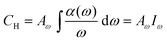
To measure the dark conductivity (σdark), films deposited on glass substrates of dimensions 3 cm × 1 cm were taken and aluminium electrodes 0.5 mm apart were deposited by thermal evaporation using a suitable mask. A constant DC voltage of ∼60 V was applied to the electrodes and current passing through the film was measured by a source meter (Keithley, 2400). The measurements were carried out at room temperature and atmospheric pressure. The charge carrier activation energy (Eact) was calculated from the temperature dependent dark conductivity measurements between 300 K and 423 K using the relation, | (1) |
Where k is the Boltzmann constant and T is the absolute temperature. The carrier concentration and mobility were calculated by Hall measurement at room temperature using Van de Pauw geometry in a field of strength 0.55 Tesla. High resolution transmission electron micrographs (HR-TEM) and selected area electron diffraction (SAED) patterns were obtained by means of a TECNAI G2-20-TWIN transmission electron microscope operating at 200 kV. The FTIR spectra were recorded in transmission mode by using a FTIR spectrophotometer (JASCO, 6100-type A) and the bonded hydrogen content (CH) was calculated using the method proposed by Brodsky et al.25 The band gap was determined with the help of a UV-Visible spectrophotometer and plotting the Tauc's curve.26 The Raman spectra were recorded by Raman spectroscopy (Jobin Yvon Horibra) in backscattering geometry. The X-ray diffraction pattern was obtained by Bruker D8 Advance X-ray diffractometer at a grazing angle of 1°. The thickness of the films was determined directly by profilometer (KLA Tencor, P-16+) and was further confirmed by UV-Visible spectroscopy using the method proposed by Swanepoel.27 Finally, the energy conversion efficiency of the solar cell was examined by means of a current–voltage (I–V) measurement under one sun illumination provided by a standard solar simulator (Oriel® Sol 2A Class AA).
3 Results and discussion
3.1 Variation in deposition rate
The variation of deposition rate (rd) plotted as a function of PH3 gas-phase ratio (ϕPH3) is shown in Fig. 1. As seen from the figure, the deposition rate increases from 10.1 Å s−1 to 12.9 Å s−1 when the PH3 gas phase-ratio increases from 1.8% to 13%. The increase in deposition rate can be attributed to an increase in density of the precursors due to an increase in the PH3 gas-phase ratio.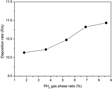 | ||
| Fig. 1 Variation of deposition rate as a function of PH3 gas-phase ratio for phosphorous doped nc-Si:H films deposited by the HW-CVD method. | ||
It is interesting to note that the deposition rate obtained in the present study for the PH3 doped nc-Si:H films is somewhat higher than the previously reported PH3 doped nc-Si:H films, compared to the conventional plasma enhanced chemical vapour deposition (PE-CVD) technique (∼0.75 Å s−1),28 microwave plasma enhanced chemical vapour deposition (MW-PE-CVD) (∼0.15 Å s−1)29 and the very recently reported low-frequency (460 kHz) inductively coupled plasma assisted chemical vapour deposition (LFIC-PA-CVD) technique (∼2.9–5.3 Å s−1).30
3.2 Micro-structural properties
Fig. 2 shows the micrograph of high resolution transmission electron microscopy (HR-TEM) for the phosphorous doped nc-Si:H films at different PH3 gas-phase ratios (ϕPH3). The corresponding selected area electron diffraction (SAED) patterns of the films are also shown in the figure.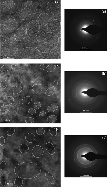 | ||
| Fig. 2 The micrographs of high resolution transmission electron microscopy (HR-TEM) for the n-type nc-Si:H thin film deposited at different PH3 gas-phase ratios, (a) ϕPH3 = 1.8%, (b) ϕPH3 = 5.3% and (c) ϕPH3 = 8.6% (left side). Some of the nano-crystallites are circled for easier recognition. The corresponding selected area diffraction (SAED) patterns of the films are also shown in the figure (right side). | ||
The nanocrystalline grains are circled in white for easier recognition. The average crystallite size of the spherical nanocrystalline silicon varies from 5 nm to 20 nm. This crystallite size is about the same, with the average crystallite size estimated from the low angle XRD pattern (discussed later) for the films depositing corning glass substrates under the same deposition conditions. From the micrograph, the nanocrystalline silicon grains surrounded by the amorphous silicon matrix are observed clearly. The representative HR-TEM images show that all the investigated samples contain a large number of randomly oriented crystallite grains of different sizes and shapes. The characteristic spotty rings SAED pattern signifies a good quality and, in general, dense polycrystalline material. The SAED pattern also reveals that the nanocrystalline silicon grains preferentially grow in the (111) orientation and then in the (220) and (311) plane directions. Thus, crystallites have more than one crystalline orientation, even for the films deposited at lower phosphine gas-phase ratios. The shape of the crystallites seems to be almost spherical with an average size between 5–20 nm. The estimated average lattice spacing using HR-TEM is ∼0.3 nm, which corresponds to the c-Si (111) plane. This supports the preferred orientation of the c-Si (111) plane that was shown by our low angle XRD results. Orientations (220) and (311) are also seen, but their peak intensity is less significant compared to the (111) plane orientation.
To get more information about the microstructure of the phosphorous doped nc-Si:H films, the Raman spectra of these samples with different PH3 gas-phase ratios (ϕPH3) are shown in Fig. 3. One can see from Fig. 3 that all the spectra deviate to different extents from the case of the single crystalline phase, where the unique peak, located at ∼520 cm−1, is present. This means that there is an amorphous or intermediate phase present in the films.
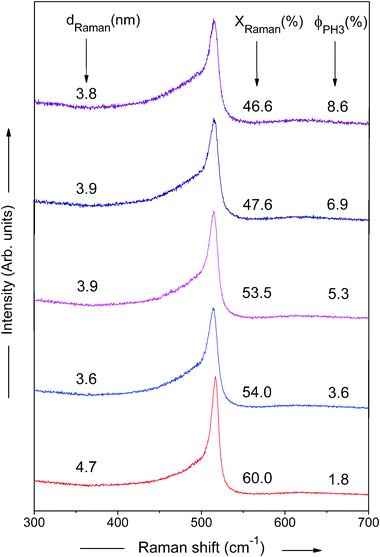 | ||
| Fig. 3 Raman spectra of phosphorous doped nc-Si:H films deposited by HW-CVD at different PH3 gas-phase ratios. | ||
Normally, the Raman spectrum is de-convoluted into three peaks. For de-convoluting the Raman spectra we have used the XPS peak fitting program, XPSPEAK Version 4.0. After fitting all the Raman spectra, we have found the best fit for two Gaussian peaks and one Lorentzian peak with minimal error. The measured Raman scattering spectra are therefore de-convoluted into two Gaussian peaks and one Lorentzian peak in the wavelength range 400–540 cm−1 using the Levenberg–Marquardt method.31 The typical de-convoluted Raman spectrum for the film deposited at ϕPH3 = 5.3% is shown in Fig. 4. The crystalline fraction (XRaman) was then calculated by,32
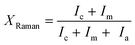 | (2) |
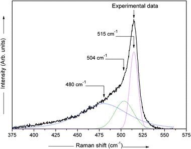 | ||
| Fig. 4 De-convoluted Raman spectrum for an n-type nc-Si:H film prepared at ϕPH3 = 5.3%, with two Gaussian peaks and one Lorentzian peak and a quadratic base line, with an algorithm based on the Levenberg–Marquardt method.31 | ||
Where Ic is the integrated intensity of the crystalline phase near 520 cm−1, Im is the integrated intensity of the intermediate phase around 500 cm−1 and Ia is the integrated intensity of the amorphous phase at 480 cm−1. The crystallite size (dRaman) was deduced using the following formula,33
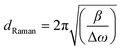 | (3) |
To further identify the crystallinity and the average crystallite size in PH3 doped nc-Si:H films, low angle X-ray diffraction (XRD) studies were carried out. The low angle XRD patterns of the nc-Si:H films deposited at different PH3 gas-phase ratios (ϕPH3) are shown in Fig. 5. It is evident from the figure that the film deposited at ϕPH3 = 1.8% is nanocrystalline, having three distinct peaks at 2θ ∼28.4°, 47.5° and 56.1°, corresponding to the (111), (220) and (311) crystal orientations, respectively. The dominant peak is (111), indicating that the crystallites in the film have a preferential orientation in the (111) direction. These results are also consistent with HR-TEM investigations. From the peak width of the (111) crystallographic plane, the average crystallite size (dX-ray) of the phosphorous doped nc-Si:H thin film can be estimated using the well known Debye–Scherrer formula,34
 | (4) |
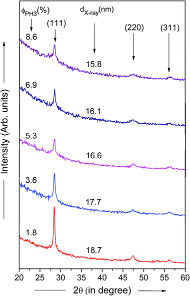 | ||
| Fig. 5 Low angle X-ray diffraction patterns of phosphorous doped nc-Si:H films deposited by HW-CVD at different PH3 gas-phase ratios. | ||
In order to investigate the hydrogen bonding configuration and to estimate the total hydrogen content in the film, Fourier transform infrared spectroscopy (FTIR) spectroscopy was used. Fig. 6 shows the FTIR spectra of the films (normalized to thickness) deposited by HW-CVD at various PH3 gas-phase ratios (ϕPH3). For clarity, the spectra have been broken horizontally into two parts.
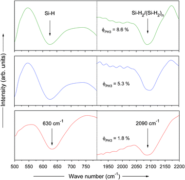 | ||
| Fig. 6 FTIR spectra of phosphorous doped nc-Si:H films deposited by HW-CVD at different PH3 gas-phase ratios at normalized thickness. | ||
Two characteristic hydrogen related modes located at ∼630 cm−1 and ∼2090 cm−1 were observed. The former is attributed to the rocking/wagging vibrational modes of different bonding configurations and the latter corresponds to the stretching vibrational modes of di-hydrogen species (Si–H2) and poly-hydrogen (Si–H2)n complexes (isolated or coupled).36 In addition to these, a broad mode located in the range 850–950 cm−1 is also observed (not shown) in the spectra for all the thin films. This mode is associated with the bending vibrational mode of the di-hydrogen species (Si–H2).37
It was found that the hydrogen content in Si:H materials is quite different depending on the technique used to calculate it. However, it has been reported that the integrated intensity of the peak ∼630 cm−1 is the best measure of hydrogen content and that other bands are less reliable.38 Whatever may be the nature of the hydrogen bonding configuration, Si–H, Si–H2, SiH3, (Si–H2)n, and so forth, all types of vibrational mode will contribute to the 630 cm−1 absorption band.39 The absorption coefficient, α, can be obtained by the Beer–Lambert law, T = Toe−α(x)d, where d is the film thickness, T and To are the transmittance of the film-substrate and the substrate, respectively, and α(ω) is the absorption coefficient at frequency ω. The hydrogen content is estimated from the absorption peak at ∼630 cm−1 because this mode is related to the entire bonded hydrogen content.38 The widely used formula is based on the integrating area, Iω, under this mode,38
 | (5) |
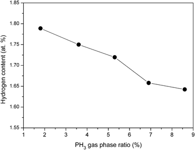 | ||
| Fig. 7 Variation in hydrogen content of phosphorous doped nc-Si:H films deposited by HW-CVD at different PH3 gas-phase ratios at normalized thickness. | ||
The hydrogen content decreases from 1.78 at% to 1.45 at% when the PH3 gas-phase ratio increases from 1.8% to 8.6%. The decrease in hydrogen content with increase in PH3 gas-phase ratio can be attributed to a decrease in volume fraction of crystallite in the films. It is well known that in nc-Si:H films, the majority of H atoms are bonded to the surface of the nanocrystallites.40 As probed by Raman and HR-TEM analysis, with increasing PH3 gas-phase ratio the density of nanocrystallite grains in the film decreases due to the decrease in volume fraction of the crystallites. This decreases the total surface area of the grains that act as reservoirs for hydrogen in the material.41 Thus, decrease in hydrogen content with increase in PH3 gas-phase ratio can be attributed to a decrease in volume fraction of crystallites in the films.
3.3 Electrical properties
Fig. 8 demonstrates the variation of dark conductivity (σdark) and its charge carrier activation energy (Eact) as a function of the PH3 gas-phase ratio. It can be seen from the figure that the dark conductivity increases from 3.71 S cm−1 to 6.78 S cm−1 and its charge carrier activation energy decreases from 0.153 eV to 0.048 eV as ϕPH3 increases from 1.8% to 5.3%. With further increase in ϕPH3, the dark conductivity decreases slightly. The charge carrier activation energy values show a reverse trend. A similar variation in dark conductivity and charge carrier activation energy of PH3 doped μc-Si:H, deposited at a filament temperature of 2500 °C by HW-CVD, has been reported previously.42 The highest value of dark conductivity achieved is 6.78 S cm−1 for the film deposited at ϕPH3 = 5.3%. This value is the highest among the so far reported dark conductivity values for phosphorous doped nc-Si:H films prepared by HW-CVD at the deposition rate 10.1 Å s−1. It is well known that the dark conductivity is determined by both the carrier concentration and the Hall mobility.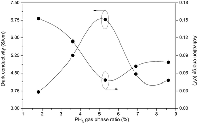 | ||
| Fig. 8 Variation of dark conductivity and its charge carrier activation energy as a function of PH3 gas-phase ratio for phosphorous doped nc-Si:H films deposited by the HW-CVD method. | ||
Fig. 9 shows the measured carrier concentration (left side) and Hall mobility (right side) at room temperature for the phosphorous doped nc-Si:H thin films with different PH3 gas-phase ratios.
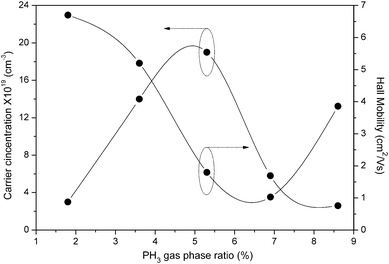 | ||
| Fig. 9 Variation of carrier concentration and Hall mobility as a function of PH3 gas-phase ratio for phosphorous doped nc-Si:H films deposited by the HW-CVD method. | ||
With regard to our n-type nc-Si:H thin films deposited by HW-CVD, the initial increase in dark conductivity is mainly attributed to the increase in carrier concentration due to the rise in the number of active dopants in the film. This is confirmed by the decrease in charge carrier activation energy that goes with a rise in dark conductivity (Fig. 8), showing that the Fermi level is moving towards the conduction band. This is consistent with a decrease in Hall mobility with an increase in the PH3 gas-phase ratio. A slight increase in PH3 gas-phase ratio beyond this optimum value (ϕPH3 = 5.3%) leads to a drastic reduction of the dark conductivity and a strong increase of the charge carrier activation energy, as shown in Fig. 8, which are indicative of leading to an amorphous material.43 This is also confirmed by Raman and XRD measurements.
3.4 UV-Visible spectroscopy analysis
Near the absorption edge, the absorption coefficient α and optical band gap Eg can be described by the following equation,| αhν ∝ (hν − Eg)γ | (6) |
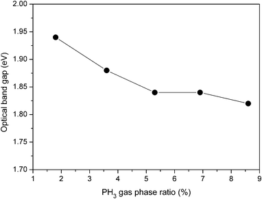 | ||
| Fig. 10 Variation of band gap as a function of PH3 gas-phase ratio for boron doped nc-Si:H films deposited by HW-CVD. | ||
It can be seen that with the increase in the PH3 gas-phase ratio from 1.8% to 8.6%, the band gap decreases from 1.94 eV to 1.86 eV. Bhattacharya et al.47 proposed that the optical band gap of the hydrogenated nanocrystalline silicon films depends on the hydrogen content and the crystalline fraction. In particular, high hydrogen content and a large crystalline fraction lead to a wider optical band gap in the nc-Si:H films deposited by the PE-CVD method. Linking the present result with the total crystallinity as revealed by Raman spectroscopy (see Fig. 3) and total amount of hydrogen by FTIR spectroscopy (see Fig. 7), the decrease in the optical band gap can be attributed to the decrease in the volume fraction of the crystallites and the decrease in hydrogen content of the films with the increase in the PH3 gas-phase ratio.
3.5 nc-Si/c-Si Heterojunction solar cell properties
To demonstrate the photovoltaic properties of the n-type nc-Si:H thin film, a heterojunction solar cell was fabricated using the configuration Al/ZnO:Al/n-nc-Si:H/buffer a-Si:H/p-c-Si/Al. The inset of Fig. 11 shows the schematic of the heterojunction solar cell fabricated in the present study.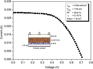 | ||
| Fig. 11 Illuminated I–V curve of the Al/ZnO:Al/nc-Si:H(n)/a-Si:H/c-Si(p)/Al heterojunction solar cell fabricated at the optimized PH3 gas-phase ratio. The inset show the schematic of the heterojunction solar cell fabricated in the present study using the HW-CVD method. | ||
Commercial Czochralski p-type c-Si (100) wafers of thickness 281 ± 25 μm and 0.01–0.02 Ω cm were used. Before deposition of the emitter, the native oxide layer on c-Si was etched away by dipping wafers in 5% diluted HF acid. The Al back metal contact was deposited on the rare side of the wafer by the method of vacuum evaporation. Then heterojunctions were fabricated by successive deposition of an a-Si:H thin buffer layer (∼5 nm) and an nc-Si:H n-layer emitter (∼180 nm) on the polished side of the Si wafer. The reasons for insertion of the a-Si:H thin buffer layer between the nc-Si:H n-layer emitter and the p-type c-Si was two-fold; firstly it possess outstanding surface passivation properties for single crystal silicon48 and secondly it enhances the formation of nucleation sites for nc-Si:H growth49 because there is a possible barrier for nanocrystalline nucleation on an amorphous i-layer surface.50 For deposition of the n-type nc-Si:H n-layer emitter, the PH3 gas-phase ratio was kept at 5.3%, for which the highest dark conductivity was obtained in the present study (see Fig. 8). A ZnO:Al (TCO) coating about 450 nm thick was deposited at 200 °C by using the pulse laser deposition (PLD) method. The top grid Al electrodes were formed by a mask vacuum evaporation technique. As the same gases with different flow rates were used for the deposition of the n-type nc-Si:H emitter and a-Si:H thin buffer layer, no evacuation was done between the deposition of the layers. Under one Sun illumination, the current–voltage (I–V) curve for the fabricated Al/ZnO:Al/n-nc-Si:H/buffer a-Si:H/p-c-Si/Al is displayed in Fig. 11. As seen from the I–V curve, the heterojunction displays excellent photovoltaic performance with an open circuit voltage (Voc) of 719 mV, a short circuit current density (Jsc) of 9.94 mA cm−2, fill factor (FF) of 53.8%, and energy conversion efficiency of ∼5.2%. The measurements were performed using a system of a Keithley 2420 sourcemeter integrated with an Oriel® Sol 2A Class AA solar simulator. The advantage of such a heterojunction solar cell is that any complicated processing, such as substrate texturing or field passivation, can be avoided in the fabrication process. The process temperature is so low (200 °C) that the degradation of the minority charge carrier is negligible, even for the low quality Si materials employed. Finally, the stability of these heterojunction solar cells can increase upon prolonged light illumination because the a-Si:H layer is very thin and contributes little to the power generation.
4 Conclusions
In summary, we have prepared phosphorous doped n-type nc-Si:H films at a low substrate temperature (200 °C) using the HW-CVD method. The effects of the PH3 gas-phase ratio on the microstructure and opto-electrical properties have been investigated by using HR-TEM, Raman scattering, low angle-XRD, FTIR spectroscopy, UV-Visible spectroscopy, temperature dependent dark conductivity and charge carrier activation energy, and Hall measurements. We found that with an increase in the PH3 gas-phase ratio, the phosphorous atoms favour growth amorphization in the nanocrystalline Si network. At the optimized PH3 gas-phase ratio, we have obtained n-type nc-Si:H films with a band gap of ∼1.84 eV and high dark conductivity (∼6.78 S cm−1) with a low hydrogen content (∼1.72 at. %) at a reasonably high deposition rate (∼10 Å s−1). As a potential application, these optimized n-type nc-Si:H incorporated into a heterojunction solar cell exhibited excellent photovoltaic properties, with Voc = 719 mV, Jsc = 9.94 mA cm−2, FF = 53.8%, and an energy conversion efficiency of 5.2%. These are very encouraging results for the future fabrication of high efficiency silicon heterojunction solar cells and thin film tandem solar cells.Acknowledgements
The authors SRJ, VSW and MMK are thankful to the Department of Science and Technology (DST) and Ministry of New and Renewable Energy (MNRE), Government of India and Centre for Nanomaterials and Quantum Systems (CNQS), University of Pune for the financial support. One of the authors VSW is also thankful to Bank of Maharashtra, University of Pune branch for the financial support.References
- C. Lee, A. Sazonov and A. Nathan, Appl. Phys. Lett., 2005, 86, 222106 CrossRef.
- H. Stiebig, E. Maulin and B. Rech, Thin Solid Films, 2007, 515, 7522 CrossRef CAS.
- J. Yang, B. Yan and S. Guha, Thin Solid Films, 2005, 487, 162 CrossRef CAS.
- R. Schropp, H. Li, R. Franken, J. Rath, C. Werf, J. Schuttauf and R. Stolk, Thin Solid Films, 2008, 516, 6818 CrossRef CAS.
- M. Ito, C. Koch, V. Svrcek, M. Schubert and J. Werner, Thin Solid Films, 2001, 383, 129 CrossRef CAS.
- M. Jana, D. Das and A. Barua, J. Appl. Phys., 2002, 91, 5442 CrossRef CAS.
- H. Zhou, D. Wei, S. Xu, S. Q. Xiao, L. X. Xu, S. Huang, Y. Guo, W. Yan and M. Xu, J. Appl. Phys., 2011, 110, 023517 CrossRef.
- S. Ishihara, D. Y. He, M. Nakata and I. Shimizu, Jpn. J. Appl. Phys., 1993, 32, 1539 CrossRef CAS.
- Y. Lubianiker, J. D. Cohen, H. C. Jin and and J. R. Abelson, Phys. Rev. B: Condens. Matter, 1999, 60, 4434 CrossRef CAS.
- Y. Hamakawa, Y. Matsumoto, G. Hirata and H. Okamoto, MRS Online Proc. LIbr., 1990, 164, 291 CAS.
- G. Yue, B. Yan, L. Sivec, T. Su, Y. Zhou, J. Yang and S. Guha, MRS Proceedings, 2012, 1426 Search PubMed.
- R. Saleh and N. H. Nickel, Thin Solid Films, 2003, 427, 266 CrossRef CAS.
- B. Pevtsov and N. A. Feoktistov, Tech. Phys. Lett., 2002, 28(4), 305 CrossRef.
- Y. He, C. Yin, G. Cheng, L. Wang, X. Liu and G. Y. Hu, J. Appl. Phys., 1994, 75, 797 CrossRef CAS.
- M. Faraji, S. V. Rajarshi, S. V. Ghaisas, S. T. Kshirsagar and V. G. Bhide, Proc. NSEC, Pune (India), 1992, 481 CAS.
- H. C. Schade, Z. E. Smith, J. H. Thomas III and A. Catalano, Thin Solid Films, 1984, 117, 149 CrossRef CAS.
- S. Major, S. Kumar, M. Bhatnagar and K. L. Chopra, Appl. Phys. Lett., 1986, 49, 394 CrossRef CAS.
- R. Schropp, J. Rath and H. Li, J. Cryst. Growth, 2009, 311(3), 760 CrossRef CAS.
- R. Stolk, H. Li, R. Franken, J. Strengers, C. Werf, J. Rath and R. Schropp, J. Non-Cryst. Solids, 2006, 352, 1933 CrossRef CAS.
- S. Klein, F. Finger, R. Carius and M. Stutzmann, J. Appl. Phys., 2005, 98, 24905 CrossRef.
- P. Gogoi, H. Jha and P. Agarwal, Thin Solid Films, 2010, 518, 6818 CrossRef CAS.
- P. Papadopulos, A. Scholz, S. Bauer, B. Shroder and H. Oechsner, J. Non-Cryst. Solids, 1993, 87, 164 Search PubMed.
- A. Mahan, J. Ca rapella, B. Nelson, R. Crandall and I. Balberg, J. Appl. Phys., 1991, 69, 6728 CrossRef CAS.
- V. Waman, M. Kamble, M. R. Pramod, A. Funde, V. Sathe, S. Gosavi and S. Jadkar, J. Nano.-Electron. Phys., 2011, 3(1), 590 Search PubMed.
- M. Brodsky, M. Cardona and J. Cuomo, Phys. Rev. B: Solid State, 1977, 16, 3556 CrossRef CAS.
- J. Tauc, in Optical Properties of Solids, ed. F. Abeles, North Holland Publication, Amsterdam, 1972 Search PubMed.
- R. Swanepoel, J. Phys. E: Sci. Instrum., 1983, 16, 1214 CrossRef CAS.
- R. Martins, A. Maqarico, I. Ferreira, R. Nunes, A. Bicho and E. Fortunato, Thin Solid Films, 1997, 303, 47 CrossRef CAS.
- B. Aken, C. Devilee, M. Dorenkamper, M. Geusebroek, M. Heijna, J. Loffler and W. Soppe, J. Non-Cryst. Solids, 2008, 354, 2392 CrossRef.
- W. Yan, D. Wei, Y. Guo, S. Xu, T. Ong and C. Sern, Thin Solid Films, 2012, 520(6), 1724 CrossRef CAS.
- D. Marquardt, J. Soc. Ind. Appl. Math., 1963, 11(2), 431 CrossRef.
- T. Kaneko, M. Wakagi, K. Onisawa and T. Minemura, Appl. Phys. Lett., 1994, 64, 1865 CrossRef CAS.
- Y. He, C. Yin, G. Cheng, L. Wang, X. Liu and G. Y. Hu, J. Appl. Phys., 1994, 75, 797 CrossRef CAS.
- H. P. Klug and L. E. Alexander, X-ray Diffraction Procedures, New York, Wiley, 1974 Search PubMed.
- S. Filonovich, M. Ribeiro, A. G. Rolo and P. Alpuim, Thin Solid Films, 2008, 516, 576 CrossRef CAS.
- W. Wei, G. Xu, J. Wang and T. Wang, Vacuum, 2007, 81, 656 CrossRef CAS.
- A. Smsts, T. Matsui and M. Kondo, Appl. Phys. Lett., 2008, 92, 033506 CrossRef.
- H. Shanks, C. Fang, L. Ley, M. Cardona, F. Demond and S. Kalbitzer, Phys. Status Solidi B, 1980, 100(1), 43 CrossRef CAS.
- W. Lau, Infrared Characterization of Microelectronics, World Scientific Publication, Singapore, 1999 Search PubMed.
- C. Arendse, G. Malgas, T. Muller, D. Knoesen, C. Oliphant, D. Motaung, S. Halindintwali and B. Mwakikunga, Nanoscale Res. Lett., 2009, 4, 307 CrossRef CAS.
- J. Baugh, D. Han, A. Kleinhammes and Y. Wu, Appl. Phys. Lett., 2001, 78, 466 CrossRef CAS.
- P. Brogueira, V. Chu, A. Ferro and J. Conde, J. Vac. Sci. Technol., A, 1997, 15, 2968 CAS.
- C. Mukherjee, U. Weber, H. Seitz and B. Schroder, Thin Solid Films, 2001, 395, 310 CrossRef CAS.
- A. Nakajima, Y. Sugita, K. Kawamura, H. Tomita and N. Yokoyama, J. Appl. Phys., 1996, 80, 4006 CrossRef CAS.
- I. Sagnes, A. Halimaoui, G. Vincent and P. A. Badoz, Appl. Phys. Lett., 1993, 62, 1155 CrossRef CAS.
- Z. Ma, X. Liao, G. Kong and J. Chu, Appl. Phys. Lett., 1999, 75, 1857 CrossRef CAS.
- K. Bhattacharya and D. Das, Nanotechnology, 2007, 18, 415704 CrossRef.
- S. Dauwe, J. Schmidt and R. Hezel, Proceeding of the 29th IEEE PVSC, New Orleans, 2002, 1246 CAS.
- F. Zignani, A. Desalvo, E. Centurioni, D. Lencinella, R. Rizzoli, C. Summonte and A. Migliori, Thin Solid Films, 2004, 451(452), 350 CrossRef.
- R. Koval, C. Chen, G. Ferreira, A. Ferlauto, J. Pearce, P. Rovira, C. Wronski and R. Collins, Appl. Phys. Lett., 2002, 81, 1258 CrossRef CAS.
| This journal is © The Royal Society of Chemistry 2012 |