Hydrothermal synthesis of CdS/CdLa2S4 heterostructures for efficient visible-light-driven photocatalytic hydrogen production
Jungang
Hou
,
Chao
Yang
,
Zheng
Wang
,
Shuqiang
Jiao
and
Hongmin
Zhu
*
School of Metallurgical and Ecological Engineering, University of Science and Technology Beijing, Beijing, 100083, China. E-mail: lorinhjg@yahoo.com.cn (J. Hou); hzhu@ustb.edu.cn (H. Zhu); Fax: +86 10 6233 4204; Tel: +86 10 6233 4775
First published on 31st August 2012
Abstract
Large-scale hydrogen production through water splitting using photocatalysts with solar energy can potentially produce clean fuel from renewable resources. In this work, photocatalytic hydrogen evolution with a high efficiency was achieved using CdS nanocrystal decorated CdLa2S4 microspheres (CdS/CdLa2S4) successfully prepared by a two-step hydrothermal process. The obtained CdS/CdLa2S4 composite was characterized by X-ray diffraction (XRD), electron microscopy (EM), X-ray photoelectron spectroscopy (XPS), UV-vis diffuse reflectance absorption spectroscopy (DRS), and photoluminescence spectroscopy (PL). XRD demonstrated that highly crystalline hexagonal CdS was obtained in CdS/CdLa2S4. EM results revealed that CdLa2S4 microspheres assembled from a large number of nanoprisms, were intimately enwrapped by the surrounding CdS nanocrystals with a particle size below 20 nm. This unique architecture resulted in the appropriate dispersion of CdS nanocrystals and intimate multipoint contacts between the CdS nanocrystals and CdLa2S4, which led to significant enhancement of charge separation in CdS/CdLa2S4. Especially, the CdLa2S4 microspheres decorated with 3 wt% CdS nanocrystals containing 0.4 wt% of Pt showed a high rate of H2-production at 2.25 mmol h−1 with an apparent quantum efficiency of 54% under 420 nm monochromatic light. The rate of hydrogen evolution from water splitting was 9 times faster in comparison with the rate observed on pure CdLa2S4, which is ascribed to the presence of CdS nanocrystals that alter the energy levels of the conduction and valence bands in the coupled semiconductor system.
1. Introduction
Photocatalytic water splitting over semiconductor photocatalysts to generate hydrogen has attracted increasing attention with sustainable energy and environment emerging as one of the top issues and challenges for humanity.1–4 In 1972, Fujishima and Honda were the first to report the use of a single-crystal TiO2 semiconductor as a photoanode for the photocatalytic decomposition of water.5 In 1976, Carey et al. successfully used TiO2 to photocatalytically degrade organic pollutants.6 TiO2 photocatalysts thus quickly attracted the attention of global environment and energy researchers. Because TiO2 is a large-band-gap semiconductor (3.0 and 3.2 eV for the rutile and anatase phases, respectively), its activation is limited only to the UV region, which accounts for only 4–5% of the spectrum of solar energy. Therefore, extending the photo-response of novel catalysts to visible light and increasing their photocatalytic efficiencies remain important future research goals.Metal sulfides are proven to be a group of highly efficient catalysts for photochemical reactions such as photocatalytic H2 evolution and reducing or oxidizing organic molecules, since photogenerated charge carriers can rapidly move to the surface of the catalysts. For example, ZnS is an important II–VI group semiconductor mostly found in two polytypes: a cubic sphalerite structure and a hexagonal wurtzite structure; with different properties.8 Besides, it is reported that hexagonal ZnS exhibits a higher ionization transition rate than cubic ZnS, while cubic ZnS is stable in the atmosphere in contrast to hexagonal ZnS.7 CdS nanostructures were demonstrated as an effective photocatalyst to degrade rhodamine B, methyl orange, and acid fuchsine and to conduct hydrogen production.8,27 Bi2S3 nanoparticles with different sizes show high efficiency in the photodegradation of rhodamine B.9 Thus, sulfides with narrow band gaps and valence bands at relatively negative potentials, can be good candidates for promising photocatalysts.
Ternary sulfides, such as ZnIn2S4 and CdLa2S4, which are members of the AB2X4 family of semiconductors with a layered structure, have attracted far-ranging interest because of their potential applications in different fields such as charge storage, thermoelectricity, photoconduction and so on.10–12 For example, Gou et al. reported that ZnIn2S4 nanotubes and nanoribbons were synthesized by a solvothermal method with pyridine as the solvent, while ZnIn2S4 solid or hollow microspheres were hydrothermally prepared in the presence of a surfactant such as cetyltrimethylammonium bromide or poly(ethylene glycol).13 Guo et al. presented that a series of ZnIn2S4 based materials exhibited high photocatalytic H2 evolution under visible light irradiation.14 Kale et al. reported that cadmium lanthanum sulfide hexagon flowers, nanoprisms and nanowires synthesized via a facile hydrothermal method, showed efficient photocatalytic activity for hydrogen production under solar light.15 Therefore, it is still a challenge to develop a new modification and/or preparation method that can enhance the photocatalytic activity of ternary sulfides.
To tackle the problem concerning the enhancement of hydrogen evolution from water splitting under visible-light irradiation, different hybrid semiconductor heterostructures have been explored. The aim has been to promote greater separation of the photoinduced charge carriers.16–19 Large numbers of efficient heterostructures for photocatalytic water splitting are reported based on different electron transfer mechanisms.20–24 For example, CdS/TiO2 heterostructures were found to exhibit a superior hydrogen evolution rate from splitting water when compared with either CdS or TiO2 alone, arising from electron transfer from the CdS conduction band (CB) to the TiO2 CB and the visible light absorption of CdS itself.20 CdS/titanate nanotubes with a unique morphology exhibited much higher activity for photocatalytic hydrogen evolution under visible light irradiation.21 Cheng et al. demonstrated that a ZnO/CdS heterostructure photocatalyst based on the direct Z-scheme mechanism exhibited a wide light response and high hydrogen evolution by prolonging the lifetime of the charge carriers.22 A CdS/MoS2 heterostructure also was shown to exhibit an enhanced photocatalytic H2 evolution under visible light irradiation.23 CdS/TaON composites showed a high visible-light-driven photocatalytic rate of H2-production from water splitting.24 In this work, we have considered the use of CdS to enhance the photoactivity of CdLa2S4, which has not been reported before to our knowledge.
It is well known that CdS is an attractive visible-light-driven photocatalyst because the CdS crystal has a conduction band edge sufficiently more negative than the reduction potential of protons and a relatively narrow band-gap, which can efficiently absorb visible light.20–24 In addition to the band-edge positions of the two semiconductors in the composite, the structure of the composite material itself can also play a critical role in determining the resulting photoconversion efficiency. Therefore, attention is paid to the structure of the CdS–CdLa2S4 composite arising from the preparation routes considered in this work.
To the best of our knowledge, no previous work regarding the application of CdS modified CdLa2S4 for photocatalytic H2 production from water splitting has been reported. Herein, we have looked at using this strategy in synergy to improve photocatalysis for hydrogen production. The CdS nanocrystal homogeneously decorated CdLa2S4 composites, were synthesized via a hydrothermal route. We have demonstrated that under visible light, the CdS/CdLa2S4 composite produced a hydrogen yield which was 9 times higher than that of pure CdLa2S4. In addition, a plausible mechanism for the photocatalytic reaction in the CdS/CdLa2S4 systems is proposed.
2. Experimental
2.1 Preparation of the pristine CdLa2S4 samples
The reagents were of analytical grade and were used without purification. Deionized (DI) water was used in all experiments. Stoichiometric amounts of Cd(NO3)2·4H2O, La(NO3)3·6H2O and double excess thiourea were mixed with 15 mL water and 5 mL ethanol. The resulting solution was added to a Teflon-lined stainless steel autoclave of 30 mL capacity and heated at 433 K for 72 h. The yellow precipitate obtained was then washed with ethanol and dried at 333 K.2.2 Preparation of CdS/CdLa2S4 composites
In a typical synthesis of the CdS/CdLa2S4 composite, an aqueous solution of Na2S·9H2O (≥98%, Aladdin) and a pre-determined amount of CdLa2S4 nanoparticles was added slowly to Cd(Ac)2·2H2O (∼98.5%, Aladdin) solution under vigorous stirring. The weight ratios of CdS to CdLa2S4 were fixed at the following values: 0, 1%, 3%, 5% and 10%, which were labelled as S0, S1, S3, S5 and S10, respectively. The resulting mixture was yellow in colour, was stirred for 24 h and kept for an additional 24 h during the ion exchange process in the next stage. The resulting yellow slurry was filtered. The wet solid was suspended in pure water (20 mL) and transferred to a Teflon-lined stainless steel autoclave (30 mL) and heated at 433 K for 24–72 h (hydrothermal treatment). After that, the yellow solid was filtered, washed with water and ethanol successively, filtered again, and then held under vacuum at 333 K for 24 h.2.3 Characterization
The obtained products were characterized with X-ray diffraction (XRD) with Cu-Ka radiation (λ = 1.54178 Å). The accelerating voltage and the applied current were 40 kV and 40 mA, respectively. Transmission electron microscopy (TEM) and high-resolution transmission electron microscopy (HRTEM) images were collected by using a JEOL model JEM 2010 EX microscope, using an accelerating voltage of 200 kV. Energy-dispersive spectroscopy (EDS) was conducted for the as-prepared samples. The optical properties of the samples were analyzed by UV-vis diffuse reflectance spectroscopy (UV-vis DRS) using a UV-vis spectrophotometer (UV2250, Shimadzu), in which BaSO4 was used as the background. The metal compositions were determined using inductively coupled plasma atomic emission spectroscopy (ICP-AES) on a Perkin Elmer ICP Optima 2000DV machine. The chemical states of the CdS/CdLa2S4 samples were determined by X-ray photoelectron spectroscopy (XPS) in a VG Multilab 2009 system (UK) with a monochromatic Al-Ka source and charge neutralizer.2.4 Photocatalytic tests
Photocatalytic hydrogen production was carried out in an air free closed gas circulation system reaction cell made of quartz. The total cylindrical volume of the cell was 200 mL. An optically polished piece of quartz glass was fused on top of the cell to minimize light scattering. Hydrogen evolution was detected using a gas chromatograph (Beijing, GC-3240, TCD, Ar carrier), which was connected to a gas-circulation line. Argon with a flow rate of 100 mL min−1 was used as a carrier gas, and was passed through the quartz glass cell.In a typical photocatalytic experiment, 0.3 g of the as-prepared CdS/CdLa2S4 photocatalysts were dispersed under constant stirring in an 200 mL mixed solution of Na2S (5 mL, 0.1 mol L−1), Na2SO3 (5 mL, 0.04 mol L−1) and DI water (190 mL). A certain amount of H2PtCl6·6H2O aqueous solution was dripped into the system to load 0.4 wt% Pt onto the surface of the photocatalysts by a photochemical reduction deposition method. The whole system, including the photocatalyst, was flushed with Ar at 100 mL min−1 for 1 h to remove any trace of air (including nitrogen and oxygen) before any photocatalytic reaction was carried out. During the process, agitation of the solution ensured uniform irradiation of the suspensions. A 0.4 mL sample of the generated gas was collected intermittently through the septum, and hydrogen content was analyzed by gas chromatography (GC-14C, Shimadzu, Japan, TCD, nitrogen as a carrier gas and a 5 Å molecular sieve column). All glassware was rigorously cleaned and carefully rinsed with distilled water prior to use.
Quantum efficiency (QE) was calculated under identical photocatalytic reaction conditions with irradiation light at λ = 420 nm by using a 300 W Xenon lamp and combined band-pass and cut-off filters, according to equations given below:
 | (1) |
Photo flux was determined by potassium ferrioxalate solution.25 The total number of incident photons was determined by measuring Fe2+ formation via the visible absorption spectroscopy of a Fe2+-phenanthroline complex at 510 nm.26 The number of incident photons was also calibrated with a Si photodiode (FZ-A, HANDY). Then photocatalytic hydrogen and oxygen generation reactions were performed using monochromatic light at 420 nm.
3. Results and discussion
3.1 Characterization of CdS/CdLa2S4 composites
The crystal structure of the pristine CdLa2S4 and CdS/CdLa2S4 composites with different weight ratios of CdS/CdLa2S4 prepared by the hydrothermal process, was analyzed by XRD patterns shown in Fig. 1. It can be seen that the distinct sharp peaks in Fig. 1a showed high crystallinity and the complete formation of the single phase CdLa2S4 nanostructures, corresponding to the major peaks at 2θ = 24.36, 30.27 and 43.8°. Besides, the ICP and EDS results (Table 1) showed that this sample has almost the same metal composition as that in the precursor solution (1![[thin space (1/6-em)]](https://www.rsc.org/images/entities/char_2009.gif) :
:![[thin space (1/6-em)]](https://www.rsc.org/images/entities/char_2009.gif) 2). Thus, it is demonstrated that there were no peaks pertaining to CdS and La2S3, which is consistent with the previous report.15
2). Thus, it is demonstrated that there were no peaks pertaining to CdS and La2S3, which is consistent with the previous report.15
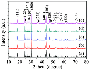 | ||
| Fig. 1 The XRD patterns of the as-prepared CdS/CdLa2S4 composites using different amounts of CdS: (a) 0, (b) 1 wt%, (c) 3 wt%, (d) 5 wt%, and (e) 10 wt%. | ||
| Sample | Weight ratio of CdS:CdLa2S4/wt% | Atomic molar ratioa of Cd2+:La3+ | Band gapb/eV | H2 production ratec/mmol h−1 | Quantum efficiencyd |
|---|---|---|---|---|---|
| a Calculated from ICP-AES and EDS results. b Calculated on the basis of the onset of the absorbance from UV-vis DRS. c Average production rate over 5 h of reaction time. d Quantum efficiency under 420 nm monochromatic light over 5 h of reaction time. | |||||
| S0 | 0 | 1.00![[thin space (1/6-em)]](https://www.rsc.org/images/entities/char_2009.gif) : :![[thin space (1/6-em)]](https://www.rsc.org/images/entities/char_2009.gif) 2 2 |
2.4–2.6 | 0.25 | 6 |
| S1 | 1 | 1.03![[thin space (1/6-em)]](https://www.rsc.org/images/entities/char_2009.gif) : :![[thin space (1/6-em)]](https://www.rsc.org/images/entities/char_2009.gif) 2 2 |
2.4–2.6 | 0.50 | 15 |
| S3 | 3 | 1.09![[thin space (1/6-em)]](https://www.rsc.org/images/entities/char_2009.gif) : :![[thin space (1/6-em)]](https://www.rsc.org/images/entities/char_2009.gif) 2 2 |
2.4–2.6 | 2.28 | 54 |
| S5 | 5 | 1.15![[thin space (1/6-em)]](https://www.rsc.org/images/entities/char_2009.gif) : :![[thin space (1/6-em)]](https://www.rsc.org/images/entities/char_2009.gif) 2 2 |
2.4–2.6 | 1.42 | 30 |
| S10 | 10 | 1.30![[thin space (1/6-em)]](https://www.rsc.org/images/entities/char_2009.gif) : :![[thin space (1/6-em)]](https://www.rsc.org/images/entities/char_2009.gif) 2 2 |
2.4–2.6 | 0.70 | 14 |
However, with increasing amounts of CdS nanocrystals, a gradual change of the intensity for several additional peaks at 2θ of 24.88, 28.28, 35.9 and 46.78° for the CdS/CdLa2S4 composites with different weight ratios of CdS to CdLa2S4, corresponding to the diffractions of the (100), (101), (102) and (103) planes of the hexagonal wurtzite phase CdS (JCPDS 89-2944) were observed in the CdS/CdLa2S4 composites, as shown in Fig. 1. In addition, the ICP and EDS results (Table 1) presented that the 3 wt% CdS nanocrystal decorated CdLa2S4 composite has a slight change in the metal composition (atomic molar ratio of Cd2+![[thin space (1/6-em)]](https://www.rsc.org/images/entities/char_2009.gif) :
:![[thin space (1/6-em)]](https://www.rsc.org/images/entities/char_2009.gif) La3+ = 1.09
La3+ = 1.09![[thin space (1/6-em)]](https://www.rsc.org/images/entities/char_2009.gif) :
:![[thin space (1/6-em)]](https://www.rsc.org/images/entities/char_2009.gif) 2) which was different with the CdLa2S4 samples. It is evident that there is nearly no change in the crystal structure of CdLa2S4 after the coating of CdS nanocrystals. Also no evident shift in the peak positions is observed in each of the as-prepared CdS/CdLa2S4 samples, suggesting the deposited CdS nanocrystals do not incorporate into the lattice of CdLa2S4.
2) which was different with the CdLa2S4 samples. It is evident that there is nearly no change in the crystal structure of CdLa2S4 after the coating of CdS nanocrystals. Also no evident shift in the peak positions is observed in each of the as-prepared CdS/CdLa2S4 samples, suggesting the deposited CdS nanocrystals do not incorporate into the lattice of CdLa2S4.
The morphologies of various samples were analyzed by TEM to directly observe the structure of the pristine CdLa2S4 and 3 wt% CdS decorated CdLa2S4 composites. It can be seen that the CdLa2S4 sample with uniform shape and size is composed of numerous submicrospheres with an average diameter of about 500 nm, as shown in Fig. 2a. Furthermore, the enlarged TEM image in Fig. 2b presented that the submicrosphere from the pristine CdLa2S4 sample was assembled with a great deal of nanoprisms, corresponding to the fairly uniform shape and size below 100 nm. The corresponding SAED pattern in Fig. 2c confirms the single-crystalline nature of the CdLa2S4 nanoprisms. The typical HRTEM image (Fig. 2d) reveals that the lattice spacing of a typical single-crystalline nanoprism from a submicrosphere is 0.293 nm. Thus, this clear lattice fringe also displays an indication of the good crystallinity of this sample.
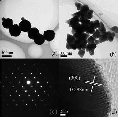 | ||
| Fig. 2 TEM images with low magnification (a) and high magnification (b), a SAED pattern recorded from a single nanoprism (c) and a HRTEM image for the pristine CdLa2S4 sample (d). | ||
Currently, it is obvious that CdS/CdLa2S4 submicrospheres presented that a number of the dispersed CdS nanocrystals are homogeneously coated on the surface of the CdLa2S4 spheres confirming the combination of CdS and CdLa2S4 composites, as shown in Fig. 3a. The enlarged image in Fig. 3b for the 3 wt% CdS decorated CdLa2S4 sample showed the size of the CdS nanocrystals in the composites is in the range of about 20 nm. In addition, the HRTEM images in Fig. 3c and Fig. 3d for this sample showed that the lattice fringes of individual CdS nanocrystals and CdLa2S4 nanoprisms with d spacings of ca. 0.245 nm and 0.293 nm, can be assigned to the (102) lattice plane of CdS and the (300) lattice plane of CdLa2S4, respectively. Therefore, the relatively small CdS nanocrystals with high crystallinity spread uniformly and tightly on the CdLa2S4 as perfect CdS/CdLa2S4 composites, indicating that CdLa2S4 is essentially interacting with CdS nanocrystals and thus inhibiting their aggregation in the hybridized composite.
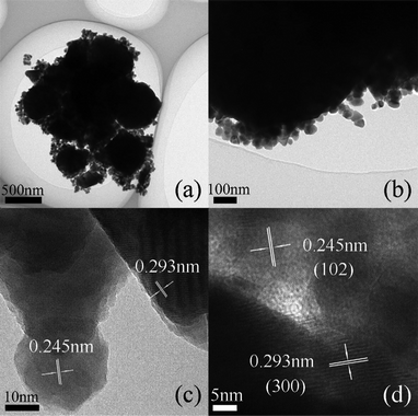 | ||
| Fig. 3 TEM images with low magnification (a) and high magnification (b), and HRTEM images for the CdS/CdLa2S4 samples (c, d). | ||
In order to reveal the very essential part of the CdS/CdLa2S4 architectures, the chemical states of the as-prepared CdS/CdLa2S4 samples were carefully checked with X-ray photoelectron spectroscopy (XPS). The XPS survey spectrum of the as-prepared CdS/CdLa2S4 composite was shown in Fig. 4a. A high-resolution XPS spectrum of the Cd 3d region was presented in Fig. 4b. XPS signals of Cd 3d were observed at binding energies of around 405.3 eV (Cd 3d5/2) and 412.0 eV (Cd 3d3/2) ascribed to Cd2+, which are consistent with the data on CdS and CdLa2S4.15,27 A high-resolution XPS spectra of the La 3d region of the catalyst was shown in Fig. 4c. The XPS signals of La 3d were observed at binding energies of around 835.5 eV (La 3d5/2), 838.8 eV (La 3d5/2) and 852.3 eV (La 3d3/2) as well as 856.0 eV (La 3d3/2), which are in good agreement with the previous work.15,28 Furthermore, XPS signals of S 2p were observed at binding energies at around 161.7 eV (S 2p3/2) and 162.8 eV (S 2p1/2) ascribed to S2−, which are consistent with the data of CdS and CdLa2S4.15–29 Besides, consistent with the ICP and EDS results, the surface ratio of Cd![[thin space (1/6-em)]](https://www.rsc.org/images/entities/char_2009.gif) :
:![[thin space (1/6-em)]](https://www.rsc.org/images/entities/char_2009.gif) La
La![[thin space (1/6-em)]](https://www.rsc.org/images/entities/char_2009.gif) :
:![[thin space (1/6-em)]](https://www.rsc.org/images/entities/char_2009.gif) S from XPS element quantitative analysis was kept unchanged for the as-prepared pristine CdLa2S4 samples and 3 mol% CdS nanocrystals decorated CdLa2S4 microspheres. Based on these observations, it is evident that a large number of nanocrystals of CdS were attached to CdLa2S4 microspheres.
S from XPS element quantitative analysis was kept unchanged for the as-prepared pristine CdLa2S4 samples and 3 mol% CdS nanocrystals decorated CdLa2S4 microspheres. Based on these observations, it is evident that a large number of nanocrystals of CdS were attached to CdLa2S4 microspheres.
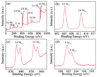 | ||
| Fig. 4 XPS spectra of a) survey spectrum, b) Cd 3d, c) La 3d and (d) S 2p for as-prepared 3 mol% CdS nanocrystal decorated CdLa2S4 submicrospheres. | ||
The UV-vis absorption spectra for CdS/CdLa2S4 samples with different amounts of CdS nanocrystals (1–10 wt%) shown in Fig. 5 were discussed. The hybridization of CdS nanocrystals with CdLa2S4 microspheres in the composites for the S0–S10 samples has resulted in absorption edge varying from 500 nm to nearly 600 nm within the visible light region. The direct band gaps of the as-prepared samples were determined according to the Kubelka–Munk method and their values are mainly distributed in the range of 2.4–2.6 eV. Light absorbance of the CdS/CdLa2S4 sample in the visible light region is of great importance for its photocatalytic application since it could be even activated by sunlight.
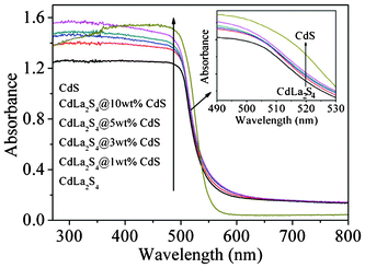 | ||
| Fig. 5 UV-vis spectra of the as-prepared CdS/CdLa2S4 composites decorated with different amounts of CdS nanocrystals. | ||
3.2 Photocatalytic activity and tentative mechanism
In this work, the CdS nanocrystal decorated CdLa2S4 composites were evaluated under visible-light irradiation for their photocatalytic H2-production activities in aqueous suspensions with Na2S and Na2SO3 as sacrificial agents. Platinum at a concentration of 0.4 wt% was employed as the electronically conducting catalyst in the redox process. As shown in Fig. 6, photocatalytic activities were confirmed for the CdS/CdLa2S4 composites among the S0–S10 samples. It is clear that the hydrogen evolution noticeably increased with the increasing content from 0 to 3 wt% of CdS nanocrystals in the CdS/CdLa2S4 composites, indicating that the 3 wt% CdS nanocrystal decorated CdLa2S4 samples exhibited the best photocatalytic hydrogen production from water splitting. However, it is worse for the photocatalytic hydrogen production when coating a large number of CdS nanocrystals above 3 wt% on the surface of the CdLa2S4 microspheres. Hence, the optimum CdS amount is about 3 wt% for the CdS/CdLa2S4 system.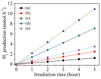 | ||
| Fig. 6 Comparison of the visible-light photocatalytic activity of the as-prepared CdS/CdLa2S4 composites decorated with different amounts of CdS nanocrystals: (a) 0, (b) 1 wt%, (c) 3 wt%, (d) 5 wt% and (e) 10 wt%. | ||
In order to obtain a comparison of photocatalytic activities, the hydrogen production rates of the as-prepared CdS/CdLa2S4 composites were shown in Fig. 7. The hydrogen production rates of the as-prepared CdS/CdLa2S4 composites for S0, S1, S3, S5 and S10 samples (Table 1), were observed for 0.25, 0.50, 2.25, 1.42 and 0.70 mmol h−1, respectively. The maximum H2 production rate was achieved for the CdS/CdLa2S4 composite (S3 sample) at a value of 2.25 mmol h−1. In addition, the apparent quantum efficiency of the as-prepared CdS/CdLa2S4 composite (S3 sample) reached the highest value of 54% at 420 nm monochromatic light and the rate exceeds that of the pristine CdLa2S4 (QE = 6%) by more than 9 times, as shown in Table 1. Therefore, the optimum content of CdS nanocrystals plays a pivotal role in the enhancement of photocatalytic performance for CdLa2S4 composites.
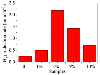 | ||
| Fig. 7 Hydrogen production rates of as-prepared CdS/CdLa2S4 composites decorated with different amounts of CdS nanocrystals. | ||
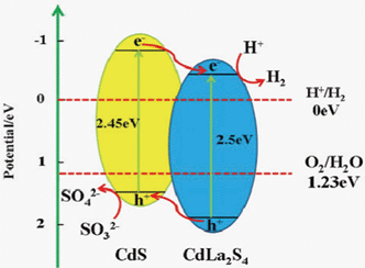 | ||
| Fig. 8 The proposed photocatalytic H2-evolution mechanism for the CdS/CdLa2S4 composite, and the calculated conduction band and valence band potentials of CdS and CdLa2S4, respectively. | ||
It is interesting to explore the possible reason for this significant increase. As schematically demonstrated in Fig. 8, charge carriers are produced when photons are irradiated onto the photocatalyst in the suspended solution. While the hole is scavenged by a mixing solution of Na2S and Na2SO3, the electron produced can be promoted to the conduction band as a result of photoexcitation. The positions of the valence band maximum (VBM) and the conduction band minimum (CBM) are critical variables in determining the feasibility of solar hydrogen production. Especially, it is important for the CB edge of a photocatalyst, to be more negative than the H+/H2 reduction potential. However, due to the large overpotential typically found in the water oxidation reaction, the band gap should be significantly larger than the theoretical redox gap. The CB and VB potentials (ECB and EVB) of CdS were determined to be ECB = −0.95 eV and EVB = 1.5 eV,8,30,31 as shown in Fig. 8. In addition, according to the following empirical equation,32,33 where EVB is the VB edge potential, X is the electronegativity of the semiconductor, which is the geometric mean of the electronegativity of the constituent atoms, Ee is the energy of free electrons on the hydrogen scale (∼4.5 eV), Eg is the band gap energy of the semiconductor, and ECB can be determined by ECB = EVB − Eg. The X value for CdLa2S4 is ca. 5.19 eV. The conduction band (CB) and valence band (VB) potentials of CdLa2S4 are -0.51 eV and 1.99 eV, respectively.
| ECB = X − Ee − 0.5Eg |
As a result, the photogenerated electrons are excited from the valence band (VB) to the conduction band (CB) of CdS, creating positive holes in the VB of CdS. As a result, the sacrificial reagents are oxidized by the positive holes in the VB of CdS and the photoexcited electrons in the CB of CdS can migrate and be injected into CdLa2S4, followed by transfer to the loaded Pt nanoparticles to generate hydrogen. Hence, the CdS/CdLa2S4 composites can increase photoactivity as a result of the efficient separation of the photogenerated electron-hole pairs, for which there is evidence in the photoluminescence spectra.
In addition, the CdS/CdLa2S4 composites containing a large number of the dispersed CdS nanocrystals might enhance the photosensitizing effect from CdS, leading to the higher absorbance for visible light. Especially, the composite exhibited a strong interaction between CdS and CdLa2S4, which could further improve the CdS photosensitization and also inhibit the recombination between photogenerated electrons and holes.
For semiconductors, the photoluminescence (PL) spectra is related to the transfer behavior of the photoinduced electrons and holes, so that it can reflect the separation and recombination of photoinduced charge carriers.34,35 The PL spectra of the CdLa2S4 and CdS/CdLa2S4 composites were shown in Fig. 9. The excitation wavelength is determined as 325 nm, and the pristine CdLa2S4 has a strong emission peak at about 518 nm. The PL intensities of CdS/CdLa2S4 composites decreased with addition of CdS nanocrystals, indicating that the electron–hole pair recombination is very slow. This is ascribed to the fact that the electrons are excited from the valence band to the conduction band of CdS and then migrate to CdLa2S4, which prevents the direct recombination of electrons and holes.
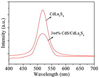 | ||
| Fig. 9 Photoluminescence spectra of CdLa2S4 and 3 wt% CdS decorated CdLa2S4 composites excited at the wavelength of 325 nm. | ||
4. Conclusions
In summary, we have successfully developed a simple hydrothermal route to reach the aim of large-scale photocatalytic hydrogen production with a high efficiency, which was achieved using CdS nanocrystal decorated CdLa2S4 microspheres. The obtained CdS/CdLa2S4 composite was characterized by XRD, EM, XPS, UV-vis and PL spectra. XRD demonstrated that highly crystalline hexagonal CdS was obtained in CdS/CdLa2S4. EM results revealed that CdLa2S4 microspheres assembled from a large number of nanoprisms, were intimately enwrapped by the surrounding CdS nanocrystals with a particle size below 20 nm. This unique architecture resulted in the appropriate dispersion of CdS nanocrystals and intimate multipoint contacts between the CdS nanocrystals and CdLa2S4, which led to significant enhancement of charge separation in CdS/CdLa2S4. Most importantly, the CdLa2S4 microspheres decorated with the homogeneously dispersed 3 wt% CdS nanocrystals containing 0.4 wt% of Pt showed a high rate of H2-production at 2.25 mmol h−1 with an apparent quantum efficiency of 54% under 420 nm monochromatic light. The rate of hydrogen evolution from water splitting was 9 times faster in comparison with the rate observed on pure CdLa2S4, which is ascribed to the presence of CdS nanocrystals that alter the energy levels of the conduction and valence bands in the coupled semiconductor system. Therefore, the present CdS/CdLa2S4 composite is promising in energy renewal, energy conversion, and environmental cleanup due to its high visible-light photoactivity.Acknowledgements
This work was supported by the National Science Foundation of China (No. 51102015, 51004008 and 21071014), the Fundamental Research Funds for the Central Universities (No. FRF-AS-11-002A and FRF-TP-12-023A), the China Postdoctoral Science Foundation (No. 20110490009), the Research Fund for the Doctoral Program of Higher Education of China (No. 20110006120027), the National Basic Research Program of China (973 Program, No. 2007CB613301) and the Program for New Century Excellent Talents in University (No. NCET-11-0577).References
- J. O. Bockris, Int. J. Hydrogen Energy, 2002, 27, 731 CrossRef CAS.
- R. M. Navarro Yerga, M. C. Alvarez Galvan, F. del Valle, J. A. Villoria de la Mano and J. L. G. Fierro, ChemSusChem, 2009, 2, 471 CrossRef CAS.
- D. Ravelli, D. Dondi, M. Fagnoni and A. Albini, Chem. Soc. Rev., 2009, 38, 1999 RSC.
- J. A. Turner, Science, 1999, 285, 687 CrossRef CAS.
- A. Fujishima and K. Honda, Nature, 1972, 238, 37 CrossRef CAS.
- J. H. Carey, J. Lawrence and H. M. Tosine, Bull. Environ. Contam. Toxicol., 1976, 16, 697 CrossRef CAS.
- (a) Y. G. Yu, G. Chen, Q. Wang and Y. X. Li, Energy Environ. Sci., 2011, 4, 3652 RSC; (b) E. Bellotti, K. rennan, R. Wang and P. Ruden, J. Appl. Phys., 1997, 82, 2961 CrossRef CAS.
- (a) W. T. Yao, S. H. Yu, S. J. Liu, J. P. Chen, X. M. Liu and F. Q. Li, J. Phys. Chem. B, 2006, 110, 11704 CrossRef CAS; (b) F. Zhang and S. S. Wong, Chem. Mater., 2009, 21, 4541 CrossRef CAS.
- T. Wu, X. G. Zhou, H. Zhang and X. H. Zhong, Nano Res., 2010, 3, 379 CrossRef CAS.
- N. Romeo, A. Dallaturca, R. Braglia and G. Sberveglieri, Appl. Phys. Lett., 1973, 22, 21 CrossRef CAS.
- W. S. Seo, R. Otsuka, H. Okuno, M. Ohta and K. Koumoto, J. Mater. Res., 1999, 14, 4176 CrossRef CAS.
- (a) Z. Lei, W. You, M. Liu, G. Zhou, T. Takata, M. Hara, K. Domen and C. Li, Chem. Commun., 2003, 2142 RSC; (b) Q. J. Xiang, J. G. Yu and M. Jaroniec, J. Am. Chem. Soc., 2012, 134, 6575 CrossRef CAS; (c) Q. Li, B. D. Guo, J. G. Yu, J. R. Ran, B. H. Zhang, H. J. Yan and J. R. Gong, J. Am. Chem. Soc., 2011, 133, 10878 CrossRef CAS; (d) J. G. Yu, J. Zhang and M. Jaroniec, Green Chem., 2010, 12, 1611 RSC.
- X. L. Gou, F. Y. Cheng, Y. H. Shi, L. Zhang, S. J. Peng, J. Chen and P. W. Shen, J. Am. Chem. Soc., 2006, 128, 7222 CrossRef CAS.
- (a) S. H. Shen, L. Zhao, Z. H. Zhou and L. J. Guo, J. Phys. Chem. C, 2008, 112, 16148 CrossRef CAS; (b) D. W. Jing, M. C. Liu and L. J. Guo, Catal. Lett., 2010, 140, 167 CrossRef CAS; (c) S. Shen, L. Zhao and L. J. Guo, Int. J. Hydrogen Energy, 2008, 33, 4501 CrossRef CAS.
- B. B. Kale, J. O. Baeg, K. J. Kong, S. J. Moon, L. K. Nikam and K. R. Patil, J. Mater. Chem., 2011, 21, 2624 RSC.
- (a) N. J. Borys, M. J. Walter, J. Huang, D. V. Talapin and J. M. Lupton, Science, 2010, 330, 1371 CrossRef CAS; (b) A. Mukherji, B. Seger, G. Q. Lu and L. Z. Wang, ACS Nano, 2011, 5, 3483 CrossRef CAS; (c) J. Zhang, J. G. Yu, Y. M. Zhang, Q. Li and J. R. Gong, Nano Lett., 2011, 11, 4774 CrossRef CAS; (d) J. Zhang, J. G. Yu, M. Jaroniec and J. R. Gong, Nano Lett., 2012 DOI:10.1021/nl301831h; (e) J. G. Hou, R. Cao, S. Q. Jiao, H. M. Zhu and R. V. Kumar, Appl. Catal. B, 2011, 101, 399 CrossRef; (f) J. G. Hou, Z. Wang, R. Cao, S. Q. Jiao and H. M. Zhu, Dalton Trans., 2011, 40, 4038 RSC; (g) J. G. Hou, Z. Wang, S. Q. Jiao and H. M. Zhu, CrystEngComm, 2012, 14, 5923 RSC.
- H. McDaniel and M. Shim, ACS Nano, 2009, 3, 434 CrossRef CAS.
- J. Y. Tang, Z. Y. Huo, S. Brittman, H. W. Gao and P. D. Yang, Nat. Nanotechnol., 2011, 6, 568 CrossRef CAS.
- (a) J. He, S. S. Lo, J. Kim and G. D. Scholes, Nano Lett., 2008, 8, 4007 CrossRef CAS; (b) Y. Y. Liang, Y. G. Li, H. L. Wang, J. G. Zhou, J. Wang, T. Regier and H. J. Dai, Nat. Mater., 2011, 10, 780 CrossRef CAS.
- L. F. Qi, J. G. Yu and M. Jaroniec, Phys. Chem. Phys. Chem., 2011, 13, 8915 CAS.
- Y. B. Chen, L. Z. Wang, G. Q. Lu, X. D. Yao and L. J. Guo, J. Mater. Chem., 2011, 21, 5134 RSC.
- X. W. Wang, G. Liu, Z. G. Chen, F. Li, L. Z. Wang, G. Q. Lu and H. M. Cheng, Chem. Commun., 2009, 3452 RSC.
- X. Zong, H. J. Yan, G. P. Wu, G. J. Ma, F. Y. Wen, L. Wang and C. Li, J. Am. Chem. Soc., 2008, 130, 7176 CrossRef CAS.
- J. G. Hou, Z. Wang, W. B. Kan, S. Q. Jiao, H. M. Zhu and R. V. Kumar, J. Mater. Chem., 2012, 22, 7291 RSC.
- J. Lee and H. H. Seliger, J. Chem. Phys., 1964, 40, 519 CrossRef CAS.
- W. S. Hummers and R. E. Offeman, J. Am. Chem. Soc., 1958, 80, 1339 CrossRef CAS.
- (a) S. K. Apte, S. N. Garaje, G. P. Mane, A. Vinu, S. D. Naik, D. P. Amalnerkar and B. B. Kale, Small, 2011, 7, 957 CrossRef CAS; (b) J. A. Villoria, R. M. N. Yerga, S. M. Al-Zahrani and J. L. G. Fierro, Ind. Eng. Chem. Res., 2010, 49, 6854 CrossRef CAS; (c) L. Schlapbach, J. Osterwalder and H. C. Siegmann, J. Less Common Met., 1982, 88, 291 CrossRef CAS.
- D. D. Sarma and C. N. R. Rao, J. Electron Spectrosc. Relat. Phenom., 1980, 20, 25 CrossRef CAS.
- Y. C. Zhang, J. Li, M. Zhang and D. D. Dionysiou, Environ. Sci. Technol., 2011, 45, 9324 CrossRef CAS.
- D. Meissner, R. Memming and B. Kastening, J. Phys. Chem., 1988, 92, 3476 CrossRef CAS.
- F. E. Osterloh, Chem. Mater., 2008, 20, 35 CrossRef CAS.
- M. A. Butler and D. S. Ginley, J. Electrochem. Soc., 1978, 125, 228 CrossRef CAS.
- X. P. Lin, J. C. Xing, W. D. Wang, Z. C. Shan, F. F. Xu and F. Q. Huang, J. Phys. Chem. C, 2007, 111, 18288 CAS.
- H. J. Huang, D. Z. Li, Q. Lin, W. J. Zhang, Y. Shao, Y. B. Chen, M. Sun and X. Z. Fu, Environ. Sci. Technol., 2009, 43, 4164 CrossRef CAS.
- (a) J. G. Hou, Z. Wang, S. Q. Jiao and H. M. Zhu, J. Hazard. Mater., 2011, 192, 1772 CrossRef CAS; (b) J. G. Hou, R. Cao, Z. Wang, S. Q. Jiao and H. M. Zhu, J. Mater. Chem., 2011, 21, 7296 RSC.
| This journal is © The Royal Society of Chemistry 2012 |
