Hierarchical branched Cu2O nanowires with enhanced photocatalytic activity and stability for H2 production†
Yuxin
Zhao
a,
Wentai
Wang
a,
Yanpeng
Li
a,
Ying
Zhang
a,
Zifeng
Yan
*a and
Ziyang
Huo
*b
aState Key Laboratory for Heavy Oil Processing, PetroChina Key Laboratory of Catalysis, China University of Petroleum, Qingdao 266580, China. E-mail: zfyancat@upc.edu.cn
bQueensland Micro- and Nanotechnology Centre, Brisbane 4111, Australia. E-mail: ziyanghuo@gmail.com
First published on 18th October 2013
Abstract
Hierarchical branched Cu2O nanowires were synthesized under mild conditions and exhibit remarkable performance for photocatalytic H2 generation from water. The obtained results open appealing perspectives for converting solar energy into storable chemical energy.
Cuprous oxide (Cu2O) is an attractive p-type oxide semi-conductor for photo-electrochemical (PEC) hydrogen production because of its direct band gap of 2.17 eV, a corresponding theoretical photocurrent of −14.7 mA cm−2 and an optimal light-to-hydrogen conversion efficiency of 18% based on the AM 1.5 spectrum.1 However, the practical application of Cu2O in the PEC process is still limited by two main drawbacks: (1) the incommensurability of the intrinsic carrier diffusion length (20–100 nm)2,3 with the light absorption depth near the band gap (approximately 10 μm)4 and (2) photo-instability in aqueous solution under illumination, as a result of self-photocorrosion.5–7 Structures based on nanowires (NWs) are known to offer a potential solution to these problems, allowing light absorption along the long axial direction and the simultaneous efficient carrier separation and collection in the nanometre-scale radial direction.8 Recent reports also found that forming complex 3-D hierarchical branched structures of 1-D systems could further improve the solar energy harvesting from that of simpler 1-D NWs, due to the major advantages of tremendously increased surface area and enhanced hetero-junction density.9,10 Up to now, extensive research efforts in photocatalytic H2 generation from water have focused on combining Cu2O with an appropriate n-type semiconductor such as TiO2, NiO, etc.,11–14 whereas the performance of Cu2O as a function of its nanoscale structural organization, has scarcely been addressed. In fact, the development of effective and low-cost preparation routes for this material, particularly with complex architectures based on NWs, is still an ongoing challenge.15,16
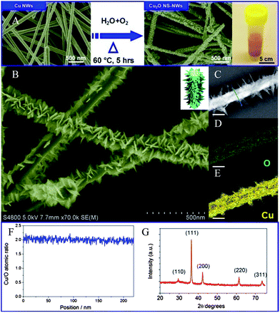
Herein we present an extremely simple strategy to synthesize a new type of hetero-structure that consists of 2-D nanosheets (NSs) and 1-D NWs, which builds on the success of the synthesis of NWs with Cu materials.17 This NS–NW hetero-structure is made by an epitaxial growth of NSs at pre-grown Cu NWs via proper oxidizing post-treatment (ambient atmosphere, 60 °C for 5 h) under humidity (65–70%), as illustrated in Fig. 1A. It exhibits a Euphorbia splendens-like structure with thin NWs as the backbone and NSs as the branches. As expected, such architectural Cu2O has shown a strong structure-induced enhancement of photocatalytic performance, including much higher photocatalytic activity as well much better durability for H2 evolution compared with the Cu2O nanoparticles (NPs) and NWs without branching structures. The as-prepared hierarchical branched Cu2O NWs could be a promising candidate for photocatalysis applications owing to its intrinsic low-cost, non-toxicity and scalability. Additionally, the primary finding of the superior photocatalytic performance of this architectural Cu2O can inspire us to further develop it in photocathode device designs.
Fig. 1B presents the high magnification SEM image of the product, which suggests that many NSs have decorated the entire NW surface, forming the hierarchical branched morphology. These on-wire NSs form sharpened irregular shapes. The lateral size of the NSs varies in a narrow range from 8 to 12 nm. However, all of the NWs show similar aspect ratios. Elemental mapping of the NS–NW was carried out using scanning transmission electron microscopy (STEM) as shown in Fig. 1C–E. Different colors indicate the presence of different elements, where yellow refers to the presence of copper and green to oxygen. Spatial distribution of the color verifies the branched structures with an inside filled nature, instead of core–shell structures or nanotubes. In addition, no obvious impurities are found on the surfaces of the samples, indicating that the as-prepared samples are relatively pure. Energy dispersive X-ray spectroscopy (EDX, Fig. S3†) confirms the presence of copper and oxygen. Using the EDX line-scanning in STEM to probe the spatial distribution of the Cu and O compositions across this single NW, we observed that the Cu/O atomic ratio of the whole NS–NW was nearly 2![[thin space (1/6-em)]](https://www.rsc.org/images/entities/char_2009.gif) :
:![[thin space (1/6-em)]](https://www.rsc.org/images/entities/char_2009.gif) 1 at all positions across the NW diameter and adjacent epitaxial NS branches (Fig. 1F). The powder X-ray diffraction (XRD) pattern of the as-obtained products confirms the material to be Cu2O, in which a set of Bragg peaks can be perfectly indexed as the pure cubic cuprite structure (Pn
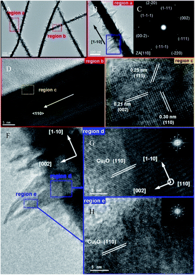
1 at all positions across the NW diameter and adjacent epitaxial NS branches (Fig. 1F). The powder X-ray diffraction (XRD) pattern of the as-obtained products confirms the material to be Cu2O, in which a set of Bragg peaks can be perfectly indexed as the pure cubic cuprite structure (Pn![[3 with combining macron]](https://www.rsc.org/images/entities/char_0033_0304.gif) m, JCPDF no. 78-2076) with lattice constant a = 4.267 Å (Fig. 1G). The corresponding transmission electron microscopy (TEM) image in Fig. 2A shows that the diameters of the Cu2O NWs are typically 90–130 nm and uniform along their length (6–8 μm). Burrs grow on the surfaces of NWs as demonstrated in the SEM characterization. Such additional branches are highly desirable for the improvement of photovoltaic performance owing to an increase in the wire surface area. Fig. 2C illustrates the corresponding selected area electron diffraction (SAED) pattern of a single NW from Fig. 2B, indicating that the Cu2O NWs are consistently single crystalline. High-resolution TEM (HRTEM) images reveal that most NWs have well-resolved (111), (110) and (002) lattice planes (Fig. 2D and E). Moreover, both HRTEM images and the assignments of SAED consistently reveal that the preferential growth direction for the Cu2O NWs is 〈110〉. The crystallographic relationship between the branched tips and the NW body were also investigated by further HRTEM imaging of the selected areas in Fig. 2F. It was found that lattice fringes mostly extend from the NW to the branched NS without any obvious lattice distortion (Fig. 2G and H). The corresponding FFT (fast Fourier transform) obtained from the junction and branch regions all show identical patterns (insets of Fig. 2G and H), suggesting that the branched hetero-structure is single crystalline throughout the entire structure. The FFT pattern also indicates that the growth direction of the NS is [002]. The consistently observed 90° angle between the branch and the body further demonstrates that the Cu2O NSs epitaxially grow from the NW along the (110) plane, resulting in single crystalline junctions with limited structural defects upon the crystal interface. The as-obtained high surface area NS–NWs and their high quality interface will significantly promote the efficiency of charge separation and consequent transition under illumination, which have been demonstrated by a photoreduction reaction.
m, JCPDF no. 78-2076) with lattice constant a = 4.267 Å (Fig. 1G). The corresponding transmission electron microscopy (TEM) image in Fig. 2A shows that the diameters of the Cu2O NWs are typically 90–130 nm and uniform along their length (6–8 μm). Burrs grow on the surfaces of NWs as demonstrated in the SEM characterization. Such additional branches are highly desirable for the improvement of photovoltaic performance owing to an increase in the wire surface area. Fig. 2C illustrates the corresponding selected area electron diffraction (SAED) pattern of a single NW from Fig. 2B, indicating that the Cu2O NWs are consistently single crystalline. High-resolution TEM (HRTEM) images reveal that most NWs have well-resolved (111), (110) and (002) lattice planes (Fig. 2D and E). Moreover, both HRTEM images and the assignments of SAED consistently reveal that the preferential growth direction for the Cu2O NWs is 〈110〉. The crystallographic relationship between the branched tips and the NW body were also investigated by further HRTEM imaging of the selected areas in Fig. 2F. It was found that lattice fringes mostly extend from the NW to the branched NS without any obvious lattice distortion (Fig. 2G and H). The corresponding FFT (fast Fourier transform) obtained from the junction and branch regions all show identical patterns (insets of Fig. 2G and H), suggesting that the branched hetero-structure is single crystalline throughout the entire structure. The FFT pattern also indicates that the growth direction of the NS is [002]. The consistently observed 90° angle between the branch and the body further demonstrates that the Cu2O NSs epitaxially grow from the NW along the (110) plane, resulting in single crystalline junctions with limited structural defects upon the crystal interface. The as-obtained high surface area NS–NWs and their high quality interface will significantly promote the efficiency of charge separation and consequent transition under illumination, which have been demonstrated by a photoreduction reaction.
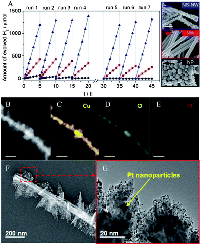
The photocatalytic properties of the as-obtained Cu2O NS–NWs and control samples (i.e. Cu2O NWs, Cu2O NPs) have been evaluated for their H2 production from aqueous solution under UV-vis light irradiation. To accelerate the H2 photogeneration process, a sacrificial agent (i.e. Na2S/Na2SO3) was used in the current work to achieve alternatively photogenerated hole suppression. Furthermore, we also employed platinum (Pt) as co-catalyst in this study (see ESI† for Pt loading details). The loading amount of Pt is fixed at 1 wt%, which has been optimized by a corresponding test with varied loading rate (see ESI†). During the whole test process the closed gas circulation system was vacuumed every 5 hours. The corresponding results are summarized in Fig. 3A. The NS–NWs show the highest H2 yield of up to ca. 263.8 μmol h−1 as compared to ca. 89.7 and 12.9 μmol h−1 of H2 generated by Cu2O NWs and NPs, respectively. It was also found that the Cu2O NS–NWs exhibit remarkably improved photostability and long lifetimes. Cycling experiments (see ESI†) further confirmed that such a steady H2 evolution rate can be maintained until 80 h of irradiation. By contrast, both of the Cu2O NWs and NPs underwent deactivation upon prolonged utilization. In particular the Cu2O NPs almost lost their photoactivity completely after 15 h of illumination, indicating the dramatic deactivation of the Cu2O photocatalyst due to photocorrosion. The intrinsic stability of Cu2O NS–NWs was examined by X-ray photoelectron spectroscopy (XPS) after the photocatalytic reaction (Fig. S9 and 10†). The results show that the Cu2p3/2 and Cu2p1/2 peaks still appear at binding energies of 932.6 and 952.9 eV, which can be assigned to Cu2O in accordance with data in the literature.18 This suggests that Cu2O was neither reduced nor oxidized after photocatalytic reaction. Correspondingly, there was no noticeable difference in the Cu LMM Auger spectra of the samples before and after irradiation. The Auger parameter value was determined to be 916.1 eV, revealing that only Cu2O was present on the surface of tested samples.19 It is well known that the activities of the semiconductor photocatalysts depend on their structural and electronic properties, which are further governed by their dimensions, crystallinity and surface properties. For the NS–NWs, the structures have numerous sharply tapered ends and needle-like burrs. These unique geometrical features facilitate the buildup of an appreciable concentration of charged species and the rapid carrier separation within a photoexcited sample, as a result of the accumulation of electrons at pointed domains of the branched Cu2O NWs and efficient carrier collection from the terminals to a central trunk. In addition, co-catalysts act as electron conductors to extract photogenerated electrons from the semiconductors, further enhancing charge separation efficiency and limiting the self-photoreduction process.20 However, the deactivation of electrocatalyst-decorated semiconductors still remains the fundamental issue to combine efficiency with cost. The main limiting factor is likely due to less efficient interfacial interaction between co-catalysts and semiconductors. Employing complex 3-D hierarchical branched NW structures may be ideal to solve this problem. In the current study, the addition of branches to the Cu2O NWs increases the surface area, which enhances the interface with Pt nanoparticles (NPs). In fact, sufficient contact between the co-catalyst Pt and Cu2O NS–NW can be clearly observed, as shown in Fig. 3B–G. As a consequence, the photoelectrons generated at Cu2O sites are more accessible for water reduction as the surface of Cu2O becomes densely covered by Pt NPs, improving the solar energy harvesting.
In summary, we have established a simple and facile strategy for the large-scale synthesis of hierarchical branched Cu2O NWs via a solution based method. This NS–NW heterostructure is supposed to be beneficial for the large surface area and efficient separation of the photoexcited electrons and holes, thus demonstrating significantly improved activity and stability for H2 production from water. We believe it not only holds great potential in applications for solar energy conversion, but also provides a novel architecture to integrate the extraordinary properties of 1-D NWs and 2-D NSs into a 3-D space.
The authors acknowledge the National Natural Science Foundation of China (no. 50901090, and no. 21106185) and China Scholarship Council (CSC, no. 201206450026) for their funding support.
Notes and references
- A. Paracchino, V. Laporte, K. Sivula, M. Grätzel and E. Thimsen, Nat. Mater., 2011, 10, 456–461 CrossRef CAS PubMed.
- S. Hacialioglu, F. Meng and S. Jin, Chem. Commun., 2012, 48, 1174–1176 RSC.
- P. E. de Jongh, D. Vanmaekelbergh and J. J. Kelly, J. Electrochem. Soc., 2000, 147, 486 CrossRef CAS PubMed.
- C. J. Engel, T. A. Polson, J. R. Spado, J. M. Bell and A. Fillinger, J. Electrochem. Soc., 2008, 155, 37–42 CrossRef PubMed.
- M. Hara, T. Kondo, M. Komoda, S. Ikeda, J. N. Kondo, K. Domen, M. Hara, K. Shinohara and A. Tanaka, Chem. Commun., 1998, 357–358 RSC.
- P. D. Tran, S. K. Batabyal, S. S. Pramana, J. Barber, L. H. Wong and S. C. J. Loo, Nanoscale, 2012, 4, 3875–3878 RSC.
- (a) Z. Zhang and P. Wang, J. Mater. Chem., 2012, 22, 2456–2464 RSC; (b) Z. Zhang, R. Dua, L. Zhang, H. Zhu, H. Zhang and P. Wang, ACS Nano, 2013, 7, 1709 CrossRef CAS PubMed.
- A. I. Hochbaum and P. D. Yang, Chem. Rev., 2010, 110, 527–546 CrossRef CAS PubMed.
- (a) J. Y. Tang, Z. Y. Huo, S. Brittman, H. W. Gao and P. D. Yang, Nat. Nanotechnol., 2011, 6, 568 CrossRef CAS PubMed; (b) M. J. Bierman, Y. K. A. Lau, A. V. Kvit, A. L. Schmitt and S. Jin, Science, 2008, 320, 1060–1063 CrossRef CAS PubMed.
- Z. Y. Huo, C. Chen, X. W. Liu, D. R. Chu, H. H. Li, Q. Peng and Y. D. Li, Chem. Commun., 2008, 3741 RSC.
- J. P. Yasomanee and J. Bandara, Sol. Energy Mater. Sol. Cells, 2008, 92, 348–352 CrossRef CAS PubMed.
- G. K. Mor, O. K. Varghese, R. H. T. Wilke, S. Sharma, K. Shankar, T. J. Latempa, K. S. Choi and C. A. Grimes, Nano Lett., 2008, 8, 1906–1911 CrossRef CAS PubMed.
- C. Y. Lin, Y. H. Lai, D. Mersch and E. Reisner, Chem. Sci., 2012, 3, 3482 RSC.
- S. David Tilley, et al. , Adv. Funct. Mater., 2013 DOI:10.1002/adfm201301106.
- (a) Y. Tan, X. Xue, Q. Peng, H. Zhao, T. Wang and Y. D. Li, Nano Lett., 2007, 7, 3723 CrossRef CAS; (b) X. L. Deng, S. Hong, I. Hwang, J. S. Kim, J. H. Jeon, Y. C. Park, J. Lee, S. O. Kang, T. Kawaia and B. H. Park, Nanoscale, 2012, 4, 2029 RSC.
- J. Shi, J. Li, X. Huang and Y. Tan, Nano Res., 2011, 4, 448–459 CrossRef CAS PubMed.
- F. Meng and S. Jin, Nano Lett., 2012, 12, 234 CrossRef CAS PubMed.
- K. Borgohain, N. Murase and S. Mahamuni, J. Appl. Phys., 2002, 92, 1292–1297 CrossRef CAS.
- J. Morales, J. P. Espinos, A. Caballero and A. R. Gonzalez-Elipe, J. Phys. Chem. B, 2005, 109, 7758–7765 CrossRef CAS PubMed.
- M. R. Hoffmann, S. T. Martin, W. Y. Choi and D. W. Bahnemann, Chem. Rev., 1995, 95, 69–96 CrossRef CAS.
Footnote |
| † Electronic supplementary information (ESI) available. See DOI: 10.1039/c3nr04280d |
| This journal is © The Royal Society of Chemistry 2014 |


