From 1D and 2D ZnO nanostructures to 3D hierarchical structures with enhanced gas sensing properties
Mohammad R.
Alenezi
ab,
Simon J.
Henley
a,
Neil G.
Emerson
a and
S. Ravi P.
Silva
*a
aNanoelectronics Center, Advanced Technology Institute, University of Surrey, Guildford, GU2 7XH, UK. E-mail: s.silva@surrey.ac.uk
bDepartment of Electronics, College of Technological Studies, PAAET, P.O. Box 42325 Shuwaikh, Kuwait
First published on 14th October 2013
Abstract
Facile and low cost hydrothermal routes are developed to fabricate three-dimensional (3D) hierarchical ZnO structures with high surface-to-volume ratios and an increased fraction of (0001) polar surfaces. Hierarchical ZnO nanowires (ZNWs) and nanodisks (ZNDs) assembled from initial ZnO nanostructures are prepared from sequential nucleation and growth following a hydrothermal process. These hierarchical ZnO structures display an enhancement of gas sensing performance and exhibit significantly improved sensitivity and fast response to acetone in comparison to other mono-morphological ZnO, such as nanoparticles, NWs, or NDs. In addition to the high surface-to-volume ratio due to its small size, the nanowire building blocks show the enhanced gas sensing properties mainly ascribed to the increased proportion of exposed active (0001) planes, and the formation of many nanojunctions at the interface between the initial ZnO nanostructure and secondary NWs. This work provides the route for structure induced enhancement of gas sensing performance by designing a desirable nanostructure, which could also be extended to synthesize other metal oxide nanostructures with superior gas sensing performance.
1 Introduction
Hierarchical nanostructures assembled from one-dimensional (1D) and two-dimensional (2D) nano-building blocks have stimulated great interest due to their exceptional physical and chemical properties.1–4 Such structures offer potential applications in the bottom-up fabrication of advanced functional devices, including sensors,5 photocatalysis,6 fuel cells,7 and drug release systems.8 Among these, gas sensors are of significant interest because of their essential role in a number of important fields, including industrial process control, safety systems, disease diagnoses, and environmental monitoring. For example, acetone is an effective biomarker for noninvasive diagnosis of type-I diabetes. For patients with type-I diabetes the acetone concentration in human breath increases from below 900 ppb for healthy individuals to higher than 1.8 ppm.9 Convenient and effective techniques for sensing acetone at low concentrations are highly desirable. Thus, for gas sensing materials to fit in these fields they need to have a high surface-to-volume ratio, low cost, and high chemical stability.A variety of hierarchical ZnO architectures including nanowire arrays,10 nanohelixes,11 nanopropellers,12 and tower-like nanocolumns13 have been successfully prepared via gas-phase growth.14–16 However, these synthetic methods usually induce impurities in the grown products, which is a disadvantage to the catalysts (poisoning of the catalyst) and templates in the reaction system. Practically, organic–inorganic hybrid hierarchical architectures are difficult to obtain because of this reason. Additionally, these methods typically require high temperatures (∼500 to 1100 °C) and vacuum conditions, which limit the economic viability for large scale production. These limitations have stimulated research on solution phase synthesis, which offers the potential for low cost, large scale manufacturing. Due to their low energy requirements, and safe and environmentally friendly processing conditions, the low temperature hydrothermal method is particularly attractive.
Regardless of all the advantages of the solution phase synthetic strategies in producing mono-morphological structures like nanoparticles, nanowires (NWs), nanorods, and nanodisks (NDs), it is still a challenge to use these strategies in the production of hierarchical architectures.
In this report, we develop an elegant nucleation and growth strategy to synthesize hierarchical ZnO nanowires (HZNWs) and hierarchical ZnO nanodisks (HZNDs). The two-step seeded growth approach allows stepwise control and optimization of experimental conditions and provides an opportunity for rational design and synthesis of controlled architectures in nanostructures.17,18 We also investigate the effect of morphology and structure on hierarchical ZnO nanostructures and on their gas sensing capabilities. The results show that the synthesized ZnO hierarchical nanostructures display better acetone sensing property than the initial ZnO mono-morphological nanostructures. Based on photoluminescence (PL) studies, the gas sensing response enhancement is attributed to more active centers that are obtained from the enhanced oxygen vacancy defects on the hierarchical nanostructures, which is due to several factors including the increased surface-to-volume ratio, the increased population of unconventional (0001) surface planes, and the formation of many nanojunctions at the interface between the initial ZnO nanostructure and secondary NWs.
2 Experimental details
2.1 Synthesis of ZnO nanostructures
All reagents in this work were analytical grade. To synthesize ZNWs, silicon (Si) substrates were cleaned by sonication in acetone, isopropyl alcohol (IPA), ethanol, and deionized water for 10 min each, sequentially. These were dried with nitrogen gas and baked on a hotplate at 150 °C for 5 min. The substrate was then spin coated with 5 mM zinc acetate dehydrate Zn(CH3COO)2·2H2O solution in ethanol at 1000 rpm for 30 s. The spin-cast layer on the silicon substrate was cured on a hot plate at 150 °C for 5 min to stabilize the film structure. The spin coating and curing processes were repeated five times in order to obtain a uniform film, which served as the seeding layer. Subsequently, the film was thermally annealed at 350 °C for 30 min, and then allowed to cool down. The thermal decomposition (of the zinc acetate) created ZnO nanocrystals on the substrate that act as a seed layer for subsequent ZnO array growth. The precursor solution for the hydrothermal reaction consists of 25–50 mM zinc nitrate, 12.5–25 mM hexamethylenetetramine (HMTA), and 0.35–0.45 M ammonium hydroxide. The seeded substrate was then placed in a vial that contains 15 mL of the growth solution. 5 mM polyethyleneimine (PEI) (end-capped, molecular weight 800 g mol−1 LS, Aldrich) was also added to the growth solution as a capping agent to control the diameter of the NWs. The vial was covered and then placed in an oven which had been preheated to 90 °C to start the growth of ZnO arrays. It takes several minutes for the growth solution to reach 90 °C. The vial was taken out of the oven after 24 h, and the silicon substrate transferred to a new vial containing only warm DI water for another 24 hours to dissolve PEI residuals. The substrate was then rinsed with DI water and dried in air at 150 °C for 30 min. Then, the ZNWs were uniformly suspended in deionized water (20 mL) in an ultrasonic bath.The suspension of ZNWs was mixed with fresh growth solution like the one used initially. The vial containing the mixture was kept at 90 °C for 5 h. Finally, upon completing the hydrothermal treatment a white precipitate was formed, which was washed thoroughly with ethanol and distilled water in sequence, and dried at 80 °C.
In the typical growth process for ZNDs, a mixture of 100 mM zinc sulphate (ZnSO4) and 100 mM HMTA is stirred at room temperature to make a homogeneous solution. The mixture is transferred to a vial and heated to 75 °C in an oven for 3 hours. After that the grown nanostructures are filtered and transferred to another vial containing water (20 mL).
The ZNDs were mixed with fresh growth solution like the one used to grow NWs. The vial containing the mixture was kept at 90 °C for 5 h. Finally, upon completion of the hydrothermal treatment a white precipitate was formed, which was washed thoroughly with ethanol and distilled water in sequence, and dried at 80 °C.
2.2 Characterization of the grown ZnO nanostructures
The crystal structures of the as-prepared products were analyzed by powder X-ray diffraction (XRD) using a Panalytical X-pert diffractometer with Cu Kα radiation. The morphology and crystal structure of as-prepared products were observed by SEM using a Philips XL-20 scanning electron microscope at 10 kV. Scanning transmission electron microscopy (STEM) and electron diffraction measurements were performed using a Hitachi HD2300A microscope, operating at 200 kV. STEM samples were prepared by depositing a drop of a diluted suspension of the nanostructure in ethanol on a carbon film coated copper grid. Photoluminescence (PL) spectroscopy was performed at room temperature using a Cary Eclipse spectrometer with an excitation wavelength of 325 nm. Nitrogen adsorption–desorption isotherms were measured using a surface area analyzer (QUADRASORB SI) at 77 K. The Brunauer–Emmett–Teller (BET) method was applied to calculate surface areas of ZnO nanostructures.2.3 Gas sensing properties of ZnO nanostructures
Gas sensors were fabricated by spin coating solutions containing ZnO nanostructures onto SiO2/Si substrates with pre-patterned gold electrodes. Before the measurement, the fabricated sensors were further aged at 300 °C for 2 days to improve the stability before testing. The gas sensing properties were measured using a home-made gas chamber attached to a Keithley 4200 semiconductor analyzer.The sensor response, Sg, is defined as Sg = (Ig − Ia)/Ia, where Ig is the sensor current value in the tested gas environment and Ia is the current value in air. The measurements were performed under fixed bias. The response time, tr, is defined as the time required for the current to reach 90% of the equilibrium value after injecting the gas, and the recovery time, td, is defined as the time necessary for the sensor to return to 10% above the original current value in air after releasing the gas from the test chamber.
3 Results and discussion
3.1 Morphology and structure
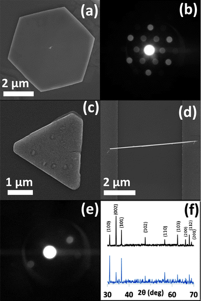
Fig. 1(a) and (b) show an SEM image and the corresponding selected area electron diffraction (SAED) pattern of a single ZND. A single ZnO nanotriangle (ZNT), a single ZNW bridging two gold electrodes and the SAED pattern of the as-grown ZNWs are shown in Fig. 1(c), (d), and (e), respectively. ZNWs are single crystals growing along the [0001] direction and their side surfaces are nonpolar {10![[1 with combining macron]](https://www.rsc.org/images/entities/char_0031_0304.gif) 0} planes. Additionally, the ZNDs are single crystals as well with their polar (0001) facet exposed. The XRD patterns of the as-grown ZNWs and ZNDs are shown in Fig. 1(f). It is found that all as-prepared structures are highly crystalline, and the diffraction peaks in every pattern can be indexed as hexagonal wurtzite-type ZnO (JCPDS no. 36-1451).
0} planes. Additionally, the ZNDs are single crystals as well with their polar (0001) facet exposed. The XRD patterns of the as-grown ZNWs and ZNDs are shown in Fig. 1(f). It is found that all as-prepared structures are highly crystalline, and the diffraction peaks in every pattern can be indexed as hexagonal wurtzite-type ZnO (JCPDS no. 36-1451).
In the hydrothermal process, ZnO tends to form 1D structures, since the crystal growth is faster along [0001] than along other directions.19 However, it was reported that changing the counter-ion for zinc often results in the production of a different crystallite morphology.20 Morphological changes may originate from the effects of the promoter species that obstructs nucleation and disrupts the growth processes. The term “crystal growth inhibition” simply refers to the change in the morphology of the crystal structure by obstructing growth on one or more facets. In the present case, the shape of the hexagonal disks and triangles is due to anisotropic growth, where the lateral growth rate is much greater than the growth rate in the c-axis direction. The (0001) and (000![[1 with combining macron]](https://www.rsc.org/images/entities/char_0031_0304.gif) ) facets of the ZnO crystal have equal reticular density but they are different in the composition of the outermost atomic layer. The effective charge is positive on the outermost layer of the (0001) facet, consisting of Zn2+ ions, while the outermost layer of the (000
) facets of the ZnO crystal have equal reticular density but they are different in the composition of the outermost atomic layer. The effective charge is positive on the outermost layer of the (0001) facet, consisting of Zn2+ ions, while the outermost layer of the (000![[1 with combining macron]](https://www.rsc.org/images/entities/char_0031_0304.gif) ) facet, consisting of O2− ions, has a negative charge of the same magnitude. Therefore, since there are no additives in our hydrothermal reaction, the counter-ions (SO42−) from the raw material could be adsorbed on the (0001) surface rather than (000
) facet, consisting of O2− ions, has a negative charge of the same magnitude. Therefore, since there are no additives in our hydrothermal reaction, the counter-ions (SO42−) from the raw material could be adsorbed on the (0001) surface rather than (000![[1 with combining macron]](https://www.rsc.org/images/entities/char_0031_0304.gif) ), substituting for hydroxyl anions and hindering the attachment of growth units of [Zn(OH)4]2− onto the (0001) surface. Consequently, the intrinsically anisotropic growth of ZnO along the (0001) direction is substantially suppressed and crystal growth then proceeds sideways forming the hexagonal disks (Fig. 1(a) and (c)). On the other hand, the effects of the other zinc counter-ions used in this work, Zn(NO3)2, were compared. The results, as expected, were 1D ZnO nanostructures as shown in Fig. 1(d).
), substituting for hydroxyl anions and hindering the attachment of growth units of [Zn(OH)4]2− onto the (0001) surface. Consequently, the intrinsically anisotropic growth of ZnO along the (0001) direction is substantially suppressed and crystal growth then proceeds sideways forming the hexagonal disks (Fig. 1(a) and (c)). On the other hand, the effects of the other zinc counter-ions used in this work, Zn(NO3)2, were compared. The results, as expected, were 1D ZnO nanostructures as shown in Fig. 1(d).
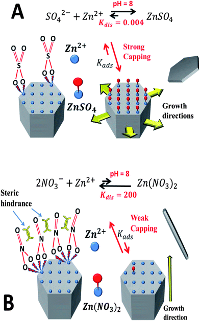
We postulate that the different morphologies that arise from the use of sulphate and nitrate are related to the ability of these counter-ions to cap the polar facet of the growing ZnO structures. The dissociation constant of ZnSO4 is much smaller than that of Zn(NO3)2 meaning that sulphate binds zinc much more energetically than two equivalent nitrate. Using the ChemEQL software, an estimate of the dissociation constants in water at a pH of 8 gives five orders of magnitude difference between the two (sulphate, Kdis = 0.004 versus nitrate, Kdis = 200) (Scheme 1).
Considering zinc terminated polar facets, it is reasonable to assume that sulphate ions will terminate much more strongly than nitrate, resulting in a strong capping effect and a slowing of the growth of the polar facet by sulphate. This effect will lead to the hexagonal disks observed. Additionally, the binding mechanism of the surface would be significantly different for sulphate and nitrate on this surface. While one sulphate ion can provide full charge balancing of the Zn2+ ion on the surface, two nitrate ions are needed to effect a similar outcome. In solution, these ions would bind the Zn2+ ion from opposite sides, but on the surface they would be forced to bind the Zn2+ ions co-facially, leading to significant steric hindrance between nitrate groups. The outcome will significantly reduce adsorption for nitrate compared to sulphate (KNO3,ad < KSO4,ad) and a poor coverage of the surface with nitrate ions. Further work will be conducted to support this theory using ab initio quantum mechanics and testing a range of counter-ions of zinc.
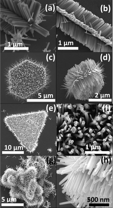
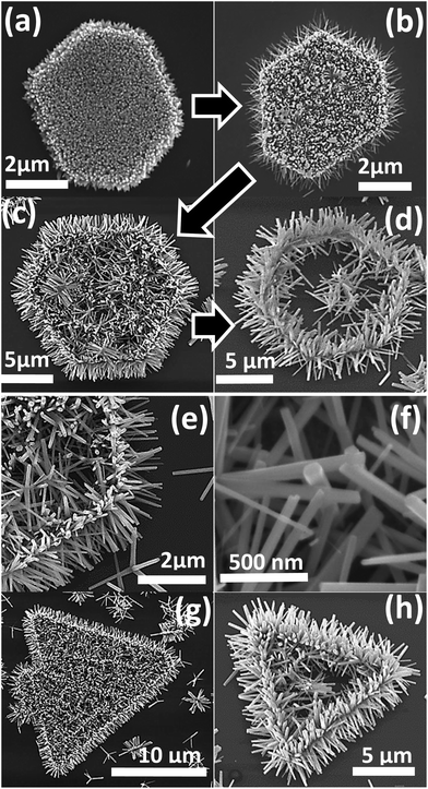
A variety of hierarchical ZnO nanostructures assembled from initial 1D and 2D ZnO nanostructures/seeds are shown in Fig. 2. The SEM images of HZNWs shown in Fig. 2(a)–(c) are observed at different magnifications. These SEM images show clearly that the secondary ZNWs are self-organized into very regular arrays forming a 6-fold symmetry. Looking closely into the morphology of the HZNWs, we observe that the secondary ZNWs grow on the side surface of the core NW. The hexagonal symmetry of the major core might be the reason for the secondary ZNWs to grow into 6-fold symmetry.21 In fact, the core NW provides its six crystal facets as growth platforms for branching of secondary NWs. Even though there are several reports on the synthesis of 6-fold ZnO nanostructures,12,21–23 the hydrothermal synthesis of these structures is rarely revealed. In the hydrothermal synthesis, heterogeneous nucleation is possible, and the interfacial energy between crystal nuclei and substrates is even smaller than that between crystal nuclei and solutions.17 Hence, secondary NWs can grow on the ZnO nanostructure central core.
Furthermore, 2D ZnO nanostructures, ZNDs and ZNTs, are used as seeds to grow hierarchical ZnO nanostructures. Top and side view SEM images of a single HZND are shown in Fig. 2(d) and (e), respectively. An SEM image of a HZNT is shown in Fig. 3(f) as well. These SEM images show that the secondary ZNWs are grown on both the top and the bottom of the initial 2D ZnO nanostructures as well as the sides. The secondary ZNWs are grown along the [0001] direction and their side surfaces are nonpolar {10![[1 with combining macron]](https://www.rsc.org/images/entities/char_0031_0304.gif) 0} planes as evident in the top view high resolution SEM image in Fig. 2(g). More careful observation of this SEM image shows that all secondary ZNWs have a flat bottom at the top, which is the polar (0001) facet. Fig. 2(h) shows low and high magnification SEM images of multiple HZNDs with high density and excellent uniformity of the secondary NWs, respectively.
0} planes as evident in the top view high resolution SEM image in Fig. 2(g). More careful observation of this SEM image shows that all secondary ZNWs have a flat bottom at the top, which is the polar (0001) facet. Fig. 2(h) shows low and high magnification SEM images of multiple HZNDs with high density and excellent uniformity of the secondary NWs, respectively.
3.2 Growth parameters
In order to meet the requirements of highly functional devices and to synthesize the best structures for gas sensing applications, we investigated the impact of the reaction conditions on the growth of hierarchical ZnO nanostructures. We started by studying the influence of the morphology of the initial ZnO nanostructures/seeds. It is found that the hierarchical ZnO nanostructures can be synthesized using seeds with a variety of different morphologies as shown in Fig. 2. Additionally, in our growth method the morphology of the initial ZnO nanostructures/seeds does not affect the aspect ratio of the secondary NWs or their density.Moreover, our studies suggest that the key factors in the growth process of the hierarchical ZnO structures are the concentration of the growth solution, growth time, and the quantity of the added PEI in the reaction system. Therefore, by understanding the influence of each one of these parameters, optimum conditions can be achieved to produce hierarchical ZnO structures that can meet the required application.
First, the concentration of the growth solution is found to control the density and average diameter of the grown secondary ZNWs. The growth solution concentration has similar effects in both cases when 1D and 2D initial ZnO nanostructures are used as seeds. However, the effect of changing the growth solution concentration is more noticeable in the case of HZNWs than in the case of HZNDs. The reason is that the 6-fold symmetry structure of the HZNWs, which is easy to observe, is very sensitive to the growth solution concentration and it can only be achieved under an optimized concentration of the growth solution (12.5–25 mM). Fig. 3(a)–(d) show SEM images of HZNWs grown at different concentrations of the growth solution. When the growth solution concentration dropped to 5 mM, only a low density of secondary ZNWs grew on each common central nucleus (Fig. 3(a)). As the growth solution concentration increased to 12.5 mM, the 6-fold brush-like hierarchical nanostructures can be seen clearly (Fig. 3(b)). Furthermore, when the solution concentration increased to around 25 mM, the amount of sub-branch ZNWs also increased, and HZNWs with high density branches could be obtained (Fig. 3(c)). It is obvious that HZNWs have lost their 6-fold brush-like structure. Clearly, this structure has a higher surface-to-volume ratio and more population of exposed polar facets than the HZNWs grown at lower growth solution concentrations.
In order to investigate the influence of the concentration of the growth solution on the density and average diameter of the secondary ZNWs grown on 2D ZnO seeds, HZNDs were grown for 2 h using different growth solution concentrations (5, 12.5, and 25 mM) which are shown in Fig. 3(e)–(g), respectively. PEI was not added to the growth solution of these HZNDs to avoid its stronger influence on the average diameter of the secondary ZNWs. It is evident from these SEM images that both the density and the average diameter increase as the growth solution concentration increases similar to the case of HZNWs.
The concentration of the growth solution (i.e., the concentration of Zn2+ and OH−) is crucial to the formation of the Zn(OH)42− precursor and hence controls the nucleation rate. At low concentrations (5 mM), only a few disordered secondary NWs grew on the most favorable nucleation sites on each common central nucleus (Fig. 3(a) and (e)). With an increase in the growth solution concentration (12.5 mM), the nucleation of ZnO was accelerated leading to more secondary NWs growing on the central nucleus (Fig. 3(b) and (f)). When the concentration was further increased (25 mM), the growth of secondary NWs was at the highest density at less optimal sites producing a more disordered morphology (Fig. 3(c) and (g)).
Moreover, the relative concentration of Zn2+ to OH− ions is also of great importance. For example when a high relative concentration of Zn2+ to OH− was used the result was similar to that of the low growth solution concentration. On the other hand, when there were excess OH− ions compared to Zn2+ ions, the OH− became not only a source of hydroxyl ions to form ZnO, but also a capping agent.24,25 The ZnO crystal is a polar solid with a positive polar plane (0001) rich in Zn and a negative polar plane (000![[1 with combining macron]](https://www.rsc.org/images/entities/char_0031_0304.gif) ) rich in O.26 At a high OH− concentration, OH− ions are preferably adsorbed on the (0001) plane of ZnO,24,27 and the growth of the ZnO nanocrystallite along the c axis is partially suppressed. It suggests that the OH− ion can act as a surface termination reagent, thus impeding the growth of the crystal face (0001).24
) rich in O.26 At a high OH− concentration, OH− ions are preferably adsorbed on the (0001) plane of ZnO,24,27 and the growth of the ZnO nanocrystallite along the c axis is partially suppressed. It suggests that the OH− ion can act as a surface termination reagent, thus impeding the growth of the crystal face (0001).24
The effect of the growth time was investigated by growing HZNWs and HZNDs for different periods of time. Fig. 4(a) and (b) show SEM images of HZNWs grown using a 12.5 mM solution concentration for 2 and 5 h, respectively. From the SEM images it can be seen that the length of the secondary ZNWs was extended, with no obvious change in their diameter. Due to the presence of PEI in our growth reaction system, the diameter is almost independent of all other factors in the reaction as discussed in the previous section. To make sure that our observations of the influence of growth time are independent of the concentration of the growth solution, the experiments were repeated with different concentrations. SEM images of HZNWs grown with 25 mM growth solution concentration for 2 and 5 h are shown in Fig. 4(c) and (d), respectively.
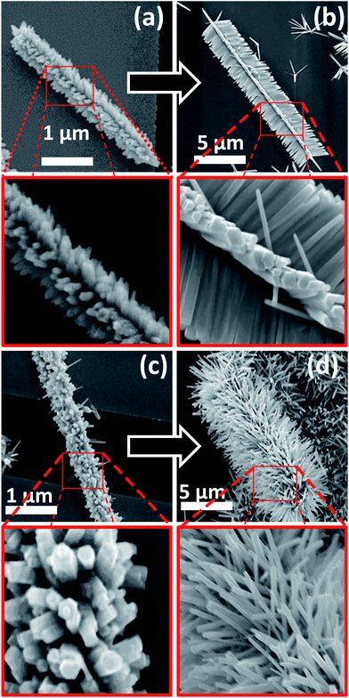 | ||
| Fig. 4 HZNWs grown with solution concentrations of (a) 12.5 mM for 2 h, (b) 12.5 mM for 5 h, (c) 25 mM for 2 h, and (d) 25 mM for 5 h. | ||
It is evident from the above SEM analysis that adjusting the growth time is an effective tool to control the length of the grown secondary NWs in the HZNW structures without affecting their density or shape. This is understood from the fact that the grown secondary NWs are covered with PEI from all exposed nonpolar facets except the top polar (0001) facet. Consequently, the growth will only continue at the exposed polar facet leading to the extension of the secondary NWs' length with no change in the diameter.
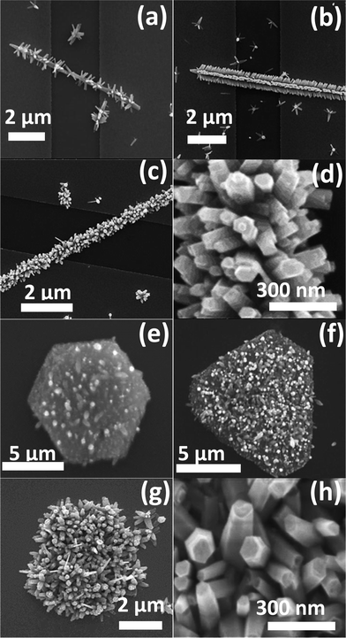
The effect of growth time on the morphology of the HZNDs can be seen from the SEM images in Fig. 5(a)–(d), where single HZNDs grown for 1, 4, 8, and 10 h are shown, respectively. The effect of growth time on the secondary NWs in this case is similar to that in the case of HZNWs. However, its influence on the HZNDs and HZNTs is not limited to the secondary NWs, but also affects the initial ZNDs and ZNTs. When the growth time is extended up to 8 h, the initial 2D ZnO seeds, ZNDs and ZNTs start to disappear as shown in Fig. 5(c) and (g), respectively, leaving behind only the grown secondary ZNWs as shown in the higher magnification SEM images in Fig. 5(e) and (f). From these images, it is clear that the secondary NWs have lost their alignment as their base is getting thinner and breaking down into pieces. Furthermore, extending the growth time beyond 8 h led to the complete disappearance of the initial seed layer and the HZNDs and HZNTs are transformed into hierarchical rings or fences as shown in Fig. 5(d) and (h).
Looking carefully into the SEM images in Fig. 5, one can see that there are two effects of the growth time on the HZNDs and HZNTs. The first effect is extending the length of the secondary NWs just like in the case of the HZNWs. The second one is dissolving the bases on which the secondary NWs are grown. Furthermore, from the SEM images of the growth process of a single HZND shown in Fig. 5(a)–(d), it is evident that only the exposed polar facets of the initial ZnO ND are affected by the dissolution process. This effect was also observed in our experiments on the transformation of ZnO NDs into ZnO nanorings by extending the growth time.
In our effort to synthesize ZnO nanostructures with an ultrahigh surface-to-volume ratio, PEI is introduced into the reaction system, and its impact on the synthesis of hierarchical ZnO structures is investigated. Our results indicate that the concentration of PEI has a significant influence on the average diameter of the secondary ZNWs grown on the hierarchical ZnO nanostructures which consequently affects the surface-to-volume ratio of the grown structures. SEM images of single HZNDs grown using different PEI concentrations of 0.5, 2, 5, and 10 mM are shown in Fig. 6(a), (c), (e) and (g), respectively. Higher resolution SEM images of the secondary NWs of the HZNDs in Fig. 6(b), (d) and (f) are also shown. It is clear that the average diameter of the secondary NWs decreases as the concentration of the PEI increases from 0.5 to 5 mM where the highest density is attained. When the PEI concentration is further increased to 10 mM, the initial ZNDs are totally encapsulated by PEI and no growth can occur on the surface due to the complete isolation from the growth solution.
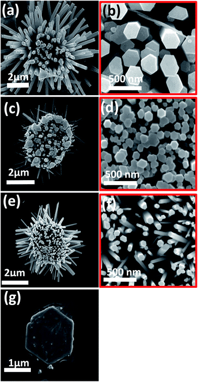 | ||
| Fig. 6 Low and high magnification SEM images of HZNDs grown with PEI concentrations of 0.5 mM (a) and (b); 2 mM (c) and (d); 5 mM (e) and (f); and 10 mM (g). | ||
It was reported in the literature that surfactants can control the morphology in the solution phase process.28–31 Among them, PEI and its ability to form nanostructures with ultrahigh aspect ratios have been studied extensively.32–34 Due to the Coulombic force between [Zn(OH)42−] and PEI, they interact to form complexes, which are adsorbed on the circumference of the ZnO nuclei. In the homogeneous nucleation case, the ZnO clusters initially formed due to thermal fluctuation are so small that the polymer chain of PEI adsorbed to certain crystal facets is long enough to cover other facets and, as a result, the steric hindrance of the PEI chain inhibits the crystal growth along all facets. Consequently, the clusters have a very small chance to grow to the critical size that thermodynamically favors the growth of crystals. On the seeded substrates, however, the preexisting seeds are large enough (5–20 nm) that despite PEI adsorption to certain crystal faces, the growing facets remain exposed to the reactants. Therefore, growth of ZnO NWs can normally occur on the seeded substrates.
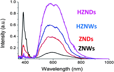
The room-temperature PL spectra of the as-grown ZnO structures with different morphologies are shown in Fig. 7. Two bands in the spectra are shown in the four cases: a luminescence band centered at 386 nm and a broadband in the region of 450–850 nm. The different structures clearly show the following intensity order for the broad luminescence band: HZNDs > HZNWs > ZNDs > ZNWs. For the peak centered at 386 nm, ZNWs have the relatively highest intensity, and the other three samples have a similar magnitude. In general, these PL spectra are similar to the ZnO PL spectra reported in the literature.35–38 The peak centered at 386 nm (3.22 eV) is generally attributed to the near band-edge emission of ZnO (3.37 eV) and the recombination of free excitons. On the other hand, it was reported that the broad band in the visible light region is a result of the oxygen vacancies at the surface of ZnO.35–38
It is well known that defects at metal oxide surfaces greatly affect the surface properties, including the reactivity of chemical adsorption, such as heterogeneous catalysis, corrosion inhibition and gas sensing.39,40 Theoretical calculations and experimental data addressing the impact of the intrinsic defects on the ZnO surface chemistry as well as the chemisorption effects have been reported.40–43 Furthermore, the mechanism of enhancing gas sensing properties of ZnO by the oxygen vacancies has been studied.44 A high density of oxygen vacancies results in a high surface adsorption of oxygen, and in turn enhances the chance of interaction with gases.
The intensity in the visible region ascribed to oxygen vacancy differs with different ZnO morphologies, HZNDs > HZNWs > ZNDs > ZNWs. This demonstrates that different ZnO morphologies have various amounts of oxygen vacancies, which decrease in turn from HZNDs, HZNWs, and ZNDs to ZNWs. Andelman et al. observed a dependency of the green band emission on ZnO morphology and suggested that the strongest green band intensity corresponded to the shape with the largest surface-to-volume ratio, which involved the largest amount of surface oxygen vacancies.38 The BET surface areas measured for the HZNDs, HZNWs, ZNDs, and ZNWs are 53.3, 41.6, 25, and 23.5 m2 g−1, respectively. Hence, based on the knowledge on the morphology and measured BET analysis, it can be noticed that the surface-to-volume ratio of the grown hierarchical ZnO structures is higher than that of their initial mono-morphological nanostructures. Interestingly, this order is consistent with the quantitative order of oxygen vacancy, suggesting there is a strong correlation between the density of oxygen vacancies and the surface-to-volume ratio of ZnO. Our observations in the current study strongly confirm the observations of Andelman et al.38
3.3 Gas sensing properties
Hierarchical metal oxide nanostructures are promising candidates as gas sensors. Their unique structures are capable of providing a large surface-to-volume ratio, which is most desirable for the diffusion of target gases in sensor materials. In addition, the formation of the initial NW–secondary NW junctions may increase the number of active sites that can enhance the response of the gas sensors. Furthermore, growing secondary NWs creates more exposed polar facets especially for the initial ZNWs with totally nonpolar exposed facets. Due to these advantages, the grown hierarchical nanostructures are expected to exhibit excellent gas sensing properties compared with those of their mono-morphological nanostructure counterparts.Four different types of gas sensors have been fabricated based on ZNWs, ZNDs, HZNWs, and HZNDs. Considering the significant influence of the operating temperature on the sensitivity of ZnO gas sensors, all fabricated sensors have been tested at different temperatures to find out the optimum operating conditions for acetone detection. Fig. 8 shows the responses of the four different sensors to 200 ppm acetone as a function of the operating temperature. The responses of sensors are found to increase with increasing the operating temperature, with the maximum responses for ZNW, ZND, HZNW, and HZND sensors being observed at 350, 375, 400, and 425 °C respectively, and then decrease with a further rise of the operating temperature. This behavior of the sensitivity as a function of the operating temperature is usually explained with regard to the kinetics and mechanics of gas adsorption and desorption on the surface of ZnO or similar semiconducting metal oxides.45 When the operating temperature is too low, the chemical activation of sensors is consequently small, leading to a very small response. When the operating temperature is increased beyond a threshold value, adsorbed gas molecules may escape before the charge transfer due to their enhanced activation, thus the response will decrease correspondingly. However, this explanation does not explain why different ZnO nanostructures have different optimum operating temperatures for the same tested gas.
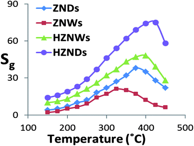 | ||
| Fig. 8 Responses of the four sensors to 200 ppm of acetone as a function of the operating temperature. | ||
The variation in the abilities of ZnO nanostructures to absorb oxygen species may be the reason behind the different optimum operating temperatures. At lower operating temperature our sensors display high resistance, which then is decreased as the operating temperature increases due to the thermal excitation of electrons. At operating temperatures above 175 °C, the resistance increases as a result of vigorous oxygen adsorptions on the ZnO surface. At this stage the oxygen chemisorption process starts competing with the thermal excitation of electrons. This competition continues until the complete coverage of the ZnO surface with chemisorbed oxygen species, where sensors show the highest sensitivity. Beyond this temperature the sensitivity starts to decrease due to the effect of the dominant thermal excitation of electrons and the saturation of oxygen adsorption on the resistance of the ZnO sensors. Fig. 8 shows that the order of the optimum operating temperature of the four sensors is temp(HZND) > temp(HZNW) > temp(ZND) > temp(ZNW), which is the same order of their ability to absorb oxygen species as confirmed by the PL analysis. Therefore, it is suggested that the optimum operating temperature of gas sensors depends significantly on the nanostructures ability to absorb oxygen species.
Curves of response versus acetone concentration of the four gas sensors are shown in Fig. 9. For acetone concentration levels of 100, 300 and 500 ppm, at its optimum operating temperature of 425 °C the HZND sensor records the highest responses of 42, 105, and 145, respectively. The HZNW sensor's responses at its optimum operating temperature of 400 °C to the same acetone levels are 25, 70 and 104, respectively, while the responses of the ZND sensor at 375 °C to the same acetone levels are 14.5, 40.5 and 61, respectively. At its optimum operating temperature of 325 °C, the sensor based on the ZNWs exhibits the weakest responses to the same levels of acetone concentration among all sensors which are 10.5, 28, and 44, respectively. It is evident that the response levels of the hierarchical ZnO structures are higher than those of the initial ZnO nanostructures over the entire range of acetone concentrations. Additionally, the sensitivity of the ZNDs is superior to that of the ZNWs.
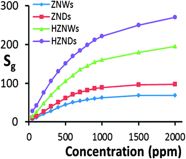 | ||
| Fig. 9 Curves of response vs. acetone concentration of the four sensors under optimum conditions (350 °C for ZNW, 375 °C for ZND, 400 °C for HZNW, and 425 °C for HZND). | ||
At acetone concentration levels above 1000 ppm, the sensitivity of the ZNW and ZND sensors shows evidence for saturation, while the sensors based on HZNDs and HZNWs are still not saturated even at 2000 ppm. This can be explained by a competition between the available adsorption sites on the surface of the ZnO nanostructure versus the concentration of acetone. When the acetone concentration level is low, the available adsorption sites are effectively infinite compared to the number of acetone molecules, and therefore the surface reaction between acetone molecules and ZnO surface is the rate-determining step. So, as long as there are enough adsorption sites, surface reactions are linearly dependent on the acetone concentration. Since the hierarchical nanostructures have a greater surface area than their initial nanostructures, they have more available adsorption sites. Consequently, the saturation of the hierarchical structure gas sensors should take place at a higher concentration level than that of their initial structures, as is observed.
Fig. 10 shows the response characteristics of the four types of ZnO sensors to an acetone concentration level of 100 ppm. The response times of ZNW, ZND, HZNW, and HZND sensors are 10, 9, 3, and 2 s, respectively, while the recovery times are 15, 14, 6, and 4 s, respectively. Clearly, the response times for the hierarchical structures are shorter than those of their initial nanostructures, and the HZND sensor has the shortest response time of all sensors. In the literature, the response time values of most oxide semiconductor gas sensors reported range from 30 to 500 s,46–49 and it is unusual to find a sensor with a response time below 10 s.
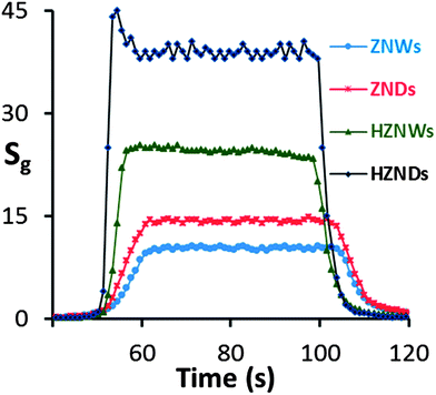 | ||
| Fig. 10 Responses of the four sensors to 100 ppm of acetone under optimum conditions (350 °C for ZNW, 375 °C for ZND, 400 °C for HZNW, and 425 °C for HZND). | ||
The response of the HZND sensor to acetone concentration levels from 1 ppm to 500 ppm is shown in Fig. 11. The HZND sensor shows an impressive performance compared not only to the other tested ZnO nanostructures in this study but also to those reported in the literature.46–50 The response time and recovery time of the HZND sensor to 5 ppm acetone are about 7 and 10 s, respectively. With the increase in acetone concentration, the response time decreases gradually for each sensor. The response times are calculated to be approximately 5 s for 20 ppm acetone and 2 s for 100 ppm. The decrease in response time can be explained by the variation of the saturation time (the time required for complete coverage of the sensor surface by the acetone molecules) and the mean residence period of acetone molecules on the HZND surface. At low levels of acetone concentration, it takes a relatively long time for acetone molecules to react with the oxygen species on the surface, leading to a longer response time. As the concentration increases, the reaction time decreases, and the response time decreases accordingly. No obvious change in recovery time can be found in our experiment, which may be due to the high operating temperature. Moreover, among the consecutive tests we realized a relatively constant base current (Ia), which demonstrates the high chemical stability.
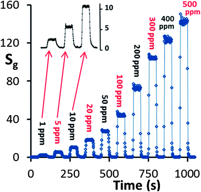 | ||
| Fig. 11 Response vs. time curve of the HZND sensor in the range of 1–500 ppm under the optimum conditions of 425 °C. | ||
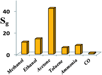
Furthermore, the selectivity of the HZND gas sensor is tested by recording its responses at the operating temperature of 425 °C to various testing gases at the concentration level of 100 ppm. Six different gases are tested, including methanol, ethanol, acetone, toluene, ammonia, and carbon monoxide. The results shown in Fig. 12 indicate that the HZND sensor exhibits low sensitivity toward toluene and ammonia and is almost insensitive toward carbon monoxide. The highest sensor response is about 42 to acetone. The sensor responses toward methanol and ethanol are about 11 and 14, respectively. It is obvious that the selectivity of the sensor to acetone against other gases is more than 3 times.
For almost all practical applications, the stability of the gas sensor device is of great importance. The HZND sensor stability has been investigated as shown in Fig. 13. It can be seen that the sensor exhibits a nearly constant sensor signal to 100, 300 and 500 ppm acetone during the test, confirming its good stability.
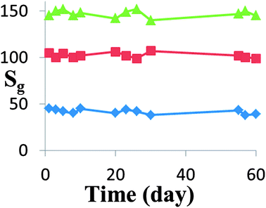 | ||
| Fig. 13 Stability of the HZND gas sensor responses to 100, 300, and 500 ppm of acetone under the optimum conditions of 425 °C. | ||
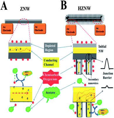
For ZnO gas sensors, the change in resistance is essentially controlled by the adsorption and desorption of gas molecules on the surface of ZnO. The mechanism of gas sensing of the single crystal ZnO nanostructures can be described by the depletion layer modulation model as depicted in part A of the schematic diagram in Scheme 2.51 When the ZnO nanostructure is in air, oxygen species are adsorbed on the surface of ZnO and capture free electrons from the conduction band forming chemisorbed oxygen species (O2−, O−, and O2−) as represented by eqn (1) and (2):
| ½O2 + e− ⇔ O− ads | (1) |
| ½O2 + 2e− ⇔ O2− ads | (2) |
When reducing gases such as acetone are introduced, the adsorbed oxygen on the ZnO surface takes part in the oxidation of acetone. The oxygen ions on the surface react with the acetone molecules and give up electrons to the conduction band and eventually increase the conductivity of the ZnO nanostructure. The overall reaction of acetone molecules with adsorbed oxygen is shown in eqn (3):52
| CH3COCH3 + 8O−(ads) ⇔ 3CO2 + 3H2O + 8e− | (3) |
However, for the hierarchical ZnO structures, there is an additional mechanism affecting the charge transport in the structure that is not available in the case of mono-morphological nanostructures. In the hierarchical ZnO structure, there are many secondary NW–initial nanostructure junctions, and electrons have to overcome the junction barrier in order to tunnel from the secondary NWs to the main ZnO nanostructure. The electron transfer barrier is formed by the surface depletion layers. The conductance of the ZNWs can be expressed as:53
| G = n0eμπ(D − 2W)2/4l | (4) |
| W = LD(eVS/kT)1/2 | (5) |
| LD = (εε0kT/e2n0)1/2 | (6) |
The enhancement in gas sensing properties of the hierarchical structures can be understood from the important aspect of surface defects. Hierarchical ZnO structures have more surface defects than their initial ZnO nanostructures, as confirmed by the PL analysis, due to the higher surface-to-volume ratio, increased population of exposed polar facets, and the formation of many secondary NW–initial NW junctions. These junctions are considered as the active sites that can enhance the response of the gas sensors.54 Therefore, a high concentration of electron donor induced oxygen vacancy defects, leading to a higher concentration of oxygen species formed on the surface of ZnO structures. This causes a larger number of electrons to be captured from the conduction band of the hierarchical ZnO structures and a thicker electron depletion layer to be formed. In other words, the resistance of the hierarchical ZnO structures is higher in air, which is a strong indication of the high sensitivity of the sensor, and the change in the resistance under acetone will be relatively larger (i.e. more sensitive).
The improvement in response time and recovery time in the hierarchical structure sensors can be attributed to the charge transport dominated by the secondary NW–initial nanostructure junction barriers. The oxygen diffusion and readsorption to deplete the ZnO nanostructure channel is a relatively slow process. The response time and recovery time will be relatively long if the device conductance is controlled by the nanostructure conductance only, while for the hierarchical structures, the conductance is controlled by the secondary NW–initial nanostructure junction barriers, which can be treated as two back-to-back tunnel barriers. The tunneling current across the junction barrier is exponentially related to the barrier height, and so is very sensitive to small changes in the barrier. Once the acetone gas is introduced the depletion layer width would decrease causing a decrease in the effective barrier due to the increased carrier density. The controlling role of the junction barrier would result in a fast current rise. Moreover, the presence of these barriers in the hierarchical structure gas sensors allows a more efficient way of blocking the electron flow compared with the mono-morphological nanostructure based gas sensors modulated only by the change in the surface depletion along the longitudinal direction.
Conclusions
In conclusion, novel hierarchical ZnO structures built by growing secondary ZNWs with controllable density on initial 1D and 2D ZnO nanostructures have been produced on a large scale through a simple and economical hydrothermal route. Control experiments reveal that the formation of these hierarchical structures depends significantly on the concentration of the growth solution as well as the growth time and PEI concentration. Essentially, the grown hierarchically structured ZnO has displayed a strong structure induced enhancement of gas sensing performance with a much better sensitivity toward acetone and fast response compared to other mono-morphological ZnO, such as ZnO nanoparticles, nanorods, and nanosheets. This is primarily attributed to their high surface-to-volume ratio, increased population of active (0001) exposed facets as well as the formation of the secondary NW–initial nanostructure junctions. These hierarchical ZnO structures are also expected to be useful for other applications such as dye-sensitized solar cells and photocatalysis.Acknowledgements
M. R. Alenezi thanks the Public Authority of Applied Education and Training (PAAET) and the Government of the State of Kuwait for their financial support. SRPS and SJH thank EPSRC for partial funding to conduct this research.Notes and references
- Z. Wang, J. Gong, Y. Su, Y. Jiang and S. Yang, Cryst. Growth Des., 2010, 10, 2455–2459 CAS
.
- M. Palumbo, T. Lutz, C. E. Giusca, H. Shiozawa, V. Stolojan, D. C. Cox, R. M. Wilson, S. J. Henley and S. R. P. Silva, Cryst. Growth Des., 2009, 9, 3432–3437 CAS
.
- K. D. G. I. Jayawardena, C. Opoku, J. Fryar, S. R. P. Silva and S. J. Henley, Appl. Surf. Sci., 2010, 257, 5274–5277 CrossRef PubMed
.
- M. McCune, W. Zhang and Y. Deng, Nano Lett., 2012, 12, 3656–3662 CrossRef CAS PubMed
.
- S. Chen and G. Sun, ACS Appl. Mater. Interfaces, 2013, 5, 6473–6477 CAS
.
- M. Zhang, C. Shao, Z. Guo, Z. Zhang, J. Mu, T. Cao and Y. Liu, ACS Appl. Mater. Interfaces, 2011, 3, 369–377 CAS
.
- Y. Qin, X. D. Wang and Z. L. Wang, Nature, 2008, 451, 809–813 CrossRef CAS PubMed
.
- H. Yang, L. Hao, N. Zhao, C. Du and Y. Wang, CrystEngComm, 2013, 15, 5760–5763 RSC
.
- M. Righettoni, A. Tricoli and S. E. Pratsinis, Anal. Chem., 2010, 82, 3581–3587 CrossRef CAS PubMed
.
- P. D. Yang, H. Q. Yan, S. Mao, R. Russo, J. Johnson, R. Saykally, N. Morris, J. Pham, R. R. He and H. Choi, Controlled Growth of ZnO Nanowires and Their Optical Properties, Adv. Funct. Mater., 2002, 12, 323–331 CrossRef CAS
.
- D. Moore, Y. Ding and Z. L. Wang, Angew. Chem., Int. Ed., 2006, 45, 5150–5154 CrossRef CAS PubMed
.
- P. X. Gao and Z. L. Wang, Appl. Phys. Lett., 2004, 84, 2883–2886 CrossRef CAS
.
- Z. R. R. Tian, J. A. Voigt, J. Liu, B. McKenzie, M. J. McDermott, M. A. Rodriguez, H. Konishi and H. F. Xu, Nat. Mater., 2003, 2, 821–826 CrossRef CAS PubMed
.
- S. H. Sun, G. W. Meng, G. X. Zhang, J. P. Masse and L. Zhang, Chem.–Eur. J., 2007, 13, 9087–9092 CrossRef CAS PubMed
.
- Q. Kuang, Z. Y. Jiang, Z. X. Xie, S. C. Lin, Z. W. Lin, S. Y. Xie, R. B. Huang and L. S. Zheng, J. Am. Chem. Soc., 2005, 127, 11777–11784 CrossRef CAS PubMed
.
- M. N. R. Ashfold, F. Claeyssens, G. M. Fuge and S. J. Henley, Chem. Soc. Rev., 2004, 33, 23–31 RSC
.
- X. P. Gao, Z. F. Zheng, H. Y. Zhu, G. L. Pan, J. L. Bao, F. Wu and D. Y. Song, Chem. Commun., 2004, 1428–1429 RSC
.
- T. L. Sounart, J. Liu, J. A. Voigt, J. W. P. Hsu, E. D. Spoerke, Z. Tian and Y. B. Jiang, Adv. Funct. Mater., 2006, 16, 335–344 CrossRef CAS
.
- X. Zhou, Z. X. Xie, Z. Y. Jiang, Q. Kuang, S. H. Zhang, T. Xu, R. B. Huang and L. S. Zheng, Chem. Commun., 2005, 5572–5574 RSC
.
- M. R. Alenezi, A. S. Alshammari, K. D. G. I. Jayawardena, M. J. Beliatis, S. J. Henley and S. R. P. Silva, J. Phys. Chem. C, 2013, 117, 17850–17858 CAS
.
- J. Y. Lao, J. G. Wen and Z. F. Ren, Nano Lett., 2002, 2, 1287–1291 CrossRef CAS
.
- J. G. Wen, J. Y. Lao, D. Z. Wang, T. M. Kyaw, Y. L. Foo and Z. F. Ren, Chem. Phys. Lett., 2003, 372, 717–722 CrossRef CAS
.
- B. Liu and H. C. Zeng, Chem. Mater., 2007, 19, 5824–5826 CrossRef CAS
.
- B. Q. Cao and W. P. Cai, J. Phys. Chem. C, 2008, 112, 680–685 CAS
.
- R. Viswanatha, H. Amenitsch and D. D. Sarma, J. Am. Chem. Soc., 2007, 129, 4470–4475 CrossRef CAS PubMed
.
- W. J. Li, E. W. Shi, W. Z. Zhong and Z. W. Yin, Growth mechanism and growth habit of oxide crystals, J. Cryst. Growth, 1999, 203, 186–196 CrossRef CAS
.
- A. Hegemann, K. Schwaebe and J. Fink, Adsorption of single Cu atoms at differently stabilized polar ZnO surfaces: An ab initio study, Comput. Chem., 2008, 29, 2302–2310 CrossRef PubMed
.
- C. L. Kuo, T. J. Kuo and M. H. Huang, J. Phys. Chem. B, 2005, 109, 20115–20121 CrossRef CAS PubMed
.
- Z. Q. Li, Y. J. Xiong and Y. Xie, Inorg. Chem., 2003, 42, 8105–8109 CrossRef CAS PubMed
.
- J. B. Liang, J. W. Liu, Q. Xie, S. Bai, W. C. Yu and Y. T. Qian, J. Phys. Chem. B, 2005, 109, 9463–9467 CrossRef CAS PubMed
.
- G. B. Sun, M. H. Cao, Y. H. Wang, C. W. Hu, Y. C. Liu, L. Ren and Z. F. Pu, Mater. Lett., 2006, 60, 2777–2782 CrossRef CAS PubMed
.
- C. K. Xu, P. Shin, L. L. Cao and D. Gao, J. Phys. Chem. C, 2010, 114, 125–129 CAS
.
- M. Law, L. Greene, J. C. Johnson, R. Saykally and P. Yang, Nat. Mater., 2005, 4, 455–459 CrossRef CAS PubMed
.
- L. E. Greene, B. D. Yuhas, M. Law, D. Zitoun and P. Yang, Inorg. Chem., 2006, 45, 7535–7543 CrossRef CAS PubMed
.
- Z. Y. Fan, P. C. Chang, J. G. Lu, E. C. Walter, R. M. Penner, C. H. Lin and H. P. Lee, Appl. Phys. Lett., 2004, 85, 6128–6131 CrossRef CAS
.
- B. Djurisic, W. C. H. Choy, V. A. L. Roy, Y. H. Leung, C. Y. Kwong, K. W. Cheah, T. K. G. Rao, W. K. Chan, H. F. Lui and C. Surya, Adv. Funct. Mater., 2004, 14, 856–864 CrossRef
.
- X. L. Wu, G. G. Siu, C. L. Fu and H. C. Ong, Appl. Phys. Lett., 2001, 78, 2285–2288 CrossRef CAS
.
- T. Andelman, Y. Y. Gong, M. Polking, M. Yin, I. Kuskovsky, G. Neumark and S. O'Brien, J. Phys. Chem. B, 2005, 109, 14314–14318 CrossRef CAS PubMed
.
- G. A. Gutierrez-Sosa, A. Baraldi, R. Larciprete and S. Lizzit, J. Am. Chem. Soc., 2002, 124, 7117–7122 CrossRef PubMed
.
- R. Lindsay, E. Michelangeli, B. G. Daniels, T. V. Ashworth, A. J. Limb and H. Geistlinger, J. Appl. Phys., 1996, 80, 1370–1381 CrossRef
.
- W. Göpel, J. Vac. Sci. Technol., 1978, 15, 1298–1311 CrossRef
.
- W. An, X. Q. Wu and X. C. Zeng, J. Phys. Chem. C, 2008, 112, 5747–5755 CAS
.
- S. Polarz, A. Roy, M. Lehmann, M. Driess, F. E. Kruis, A. Hoffmann and P. Zimmer, Adv. Funct. Mater., 2007, 17, 1385–1391 CrossRef CAS
.
- L. Liao, H. B. Lu, J. C. Li, H. He, D. F. Wang, D. J. Fu, C. Liu and W. F. Zhang, J. Phys. Chem. C, 2007, 111, 1900–1903 CAS
.
- M. Ghasdi and H. Alamdari, Sens. Actuators, B, 2010, 148, 478–485 CrossRef CAS PubMed
.
- Y. K. Jun, H. S. Kim, J. H. Lee and S. H. Hong, Sens. Actuators, B, 2006, 120, 69–73 CrossRef CAS PubMed
.
- K. Galatsis, Y. X. Li, W. Wlodarski, E. Comini, G. Faglia and G. Sberveglieri, Sens. Actuators, B, 2001, 77, 472–477 CrossRef CAS
.
- M. Kugishima, S. Sakai, K. Shimanoe and N. Yamazoe, Sens. Actuators, B, 2005, 108, 130–133 CrossRef CAS PubMed
.
- P. S. Cho, K. W. Kim and J. H. Lee, J. Electroceram., 2006, 17, 975–978 CrossRef CAS PubMed
.
- Y. Zeng, T. Zhanga, M. Yuan, M. Kang, G. Lu, R. Wang, H. Fan, Y. He and H. Yang, Sens. Actuators, B, 2009, 143, 93–98 CrossRef PubMed
.
- Z. H. Jing and J. H. Zhan, Adv. Mater., 2008, 20, 4547–4551 CrossRef CAS
.
- P. A. Murade, V. S. Sangawar, G. N. Chaudhari, V. D. Kapse and A. U. Bajpeyee, Curr Appl. Phys., 2010, 11, 451–456 CrossRef PubMed
.
- V. V. Sysoev, B. K. Button, K. Wepsiec, S. Dmitriev and A. Kolmakov, Nano Lett., 2006, 6, 1584–1588 CrossRef CAS PubMed
.
- D. H. Zhang, Z. Q. Liu, C. Li, T. Tang, X. L. Liu, S. Han, B. Lei and C. W. Zhou, Nano Lett., 2004, 4, 1919–1924 CrossRef CAS
.
| This journal is © The Royal Society of Chemistry 2014 |

