Controlled removal of monolayers for bilayer graphene preparation and visualization†
Lin Gan‡
a,
Haijing Zhang‡b,
Ruizhe Wua,
Yao Dinga,
Ping Shengb and
Zhengtang Luo*a
aDepartment of Chemical and Biomolecular Engineering, The Hong Kong University of Science and Technology, Clear Water Bay, Kowloon, Hong Kong, China. E-mail: keztluo@ust.hk
bDepartment of Physics and William Mong Institute of Nano Science and Technology, The Hong Kong University of Science and Technology, Clear Water Bay, Kowloon, Hong Kong, China
First published on 2nd March 2015
Abstract
Bilayer graphene, unlike monolayer graphene, provides a tunable electronic energy gap when an electrical field is applied across the layers, and therefore holds great potential in the semiconductor industry. Here, we demonstrate a facile technique to obtain bilayer graphene structures on the growth substrate by controlling oxidation to remove monolayers, while retaining the bilayer electronic properties. We found that this precise oxidation process selectively destructs monolayers while preserves the qualities of bilayers, evidenced by the expected quantum Hall effect and exceptional room temperature carrier mobilities of ∼3500 cm2 V−1 s−1 obtained from an electrical transport measurement. In addition, visualization of the bilayers, which serve as nuclei for graphene growth, opens the door to understanding the actual mechanism of the graphene growth process which eventually can lead to the optimized synthesis.
Introduction
Graphene is a promising material for electronic applications, but its intrinsic gapless semimetal nature hurdles its application in the semiconducting industry. On the other hand, bilayer graphene, in particular for AB Bernal stacking order, can provide a tunable bandgap when an electrical field is applied across the layers, hence forth attracting considerable attention for its potential application in logic circuits.1–3 To obtain large sized graphene thin films for practical applications, a Chemical Vapor Deposition (CVD) method4–6 was developed to synthesize monolayer graphene thin films, which was later extended for bilayers or few layer graphene preparation. However, current processes always produce graphene films that contain a significant portion of monolayer, which will have detrimental effects when used in semiconductor devices. Moreover, it would be also desirable to directly observe the structure and overall distribution of graphene nuclei during CVD growth, in order to understanding the underlying kinetics for graphene growth. Previously, a simple optical method has been developed to directly visualize monolayer graphene grains on Cu foil, taking advantage of their different contrast between graphene-covered and uncovered region after mild oxidation.7 However, visualizing bilayer graphene has not been reported so far, due to the difficulties of gaining contrast between bilayer and monolayer graphene. Consequently, characterization methods for bilayers on Cu substrate are mainly limited to localized methods such as scanning electron microscopy (SEM)8 and atomic force microscopy (AFM),9 which precludes us from obtaining a full map of graphene distribution on copper substrate, or limiting us to an optical method by transferring the post-synthesized graphene onto silicon wafer of 300 nm SiO2.10Here we show a simple method that enables us to solve the purification and direct visualization issue at the same time. This is achieved by controlling the oxidization of the post-growth monolayer and bilayer graphene/Cu substrate in air at a raised temperature, utilizing their different resistance to oxidation. Controlled oxidation renders the Cu metal covered by monolayer easily oxidized, while area covered by the bilayers are only insignificantly affected, and consequently leads to the contrast for the monolayer and bilayer covered region. Electron transport measurement on bilayer-based FET devices confirms that the quality of bilayers are well preserved during this controlled oxidation process.
Results and discussions
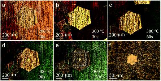
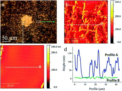
We firstly demonstrate a controlled oxidation method by showing the evolution of graphene grains during this process. Fig. 1 illustrates a sequence of optical images recorded at end of annealing at 200 °C for 30 s, followed by annealing in air at 300 °C for additional 30 s, 60 s, 90 s and 120 s, respectively. At the early stage of annealing, the contrast of monolayer to copper substrate gradually increases and reached a maximum after annealing at 300 °C for ∼60 s concurrent with the observation that copper substrate turning from red to light green in this process (for more images, see Fig. S1 of ESI†). Additional annealing at 300 °C for 90 s induces a sudden decrease in contrast between monolayers and copper substrate, while simultaneously reveals the bilayer nucleus in the center of the graphene grain. After additional annealing at 300 °C for 120 s, majority of the monolayers are broken into fragments and the nucleus stand out sharply. In addition, we note that a significant number of cracks emerge along the edges of nucleus, as shown in Fig. 1f, implying that the oxidation for nucleus may start from the edges. Similar result can be obtained if lower annealing temperature but longer duration is used, for example, after exposing the graphene/Cu sample in air for several months (Fig. S2 of ESI†), the nuclei also become visible.Fig. 2 illustrates the detailed surface morphology acquired by atomic force microscope (AFM). The after-oxidation morphology of regions that were previously covered by monolayer, i.e. in the outer part of the graphene (Fig. 2b and corresponding profile in Fig. 2d) shows that monolayer grain has been broken into fragments, possibly are damaged by the copper oxide particles or stripes formed after the oxidation, whereas the bilayer nucleus are intact with only a few insignificant damages (Fig. 2c and corresponding profile in Fig. 2d), consistent with the result shown in Fig. 1f. The formation of oxide particles or stripes after oxidation has been elaborately studied by many groups5,11,12 (also see XPS results in Fig. S6 of ESI†) and the size ranges from nanometer to micrometer scales, depending on degree of oxidation and temperature. As a result of nanoparticle's volume expansion, stress will be induced on the monolayer graphene, which also leads to their reactivity enhancement. Following the oxidation on those sites, defects and cracks will expand to larger cracks, which allows more exposure to oxygen for the Cu substrates. As shown in Fig. 2a, a crack are also occasionally seen on some bilayers regions, but typically has limited effect on electronic quality as will be shown in latter part of the discussion.
The method reported here provides insights on possible oxygen diffusion path during the oxidation. Previously study has shown that graphene is impermeable for most gas, including helium.13 Therefore, the most likely paths for oxygen to attack the graphene-covered region are (1) from above through defects or atom exchange mechanism,14 or (2) from bottom through the micro-space/ripples formed between grains and copper substrate. One would expect the former path is more common, as defective sites usually has high reactivity, as it was observed that the methane decomposition usually started at those defective sites which includes impurities,15 metal step16 or metal particles.5 This diffusion path, however, does not agree with our experimental observation that only insignificant damage were observed at the nucleus center, while the majority of cracks are near the edges. Instead, our observation supports that oxygen may attack the monolayers from underneath. Indeed, micrometer scale periodical ripples5,8 are widely seen for CVD-grown graphene due to the thermal expansion coefficient mismatch between graphene and copper substrate during cooling process. Those ripples form easy accessible channel for oxygen diffusion (Fig. S3 of ESI†). Nevertheless, the oxygen path may also dependent on the temperature, as crack and pits are also seen in the graphene terrace when the sample is placed in air at room temperature for an extended period (Fig. S2 of ESI†). In addition, electrochemical erosion may have also involved in this process.17
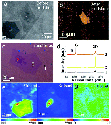
Fig. 3 depicts further characterization of the visualized bilayer/few layers graphene structure. Fig. 3a illustrates the scanning electron microscopy (SEM) image of a typical bilayer/few layers graphene flake synthesized by CVD,5 which were embedded at the center of a large single crystal graphene monolayer (inset of Fig. 3a). The monolayer graphene shows asymmetric structure of diameter ∼1 mm, consistent with our previous report. After annealing the sample in air under 300 °C for 2 minutes, intense contrast were obtained for the bilayer nucleus at the center, where the monolayer-covered region become less reflective and turned to dark color, as shown in Fig. 3b (see more images at Fig. S4 in the ESI†). As will be clarified later from Raman measurement, this originated from the destruction of the monolayer, concurrent with copper substrate oxidation. By using this method, the nucleus region stands out sharply against original graphene flake region, due to the contrast resulted from reduced reflectance. Interestingly from this visualization method, we observed some individual hexagonal shape grains have more than one nucleus in the center (ESI Fig. S2†), contrary to common belief that each graphene flake was grown from a single nucleus. More work is in progress to understand this phenomenon.
To understand the nature of graphene nucleus, we performed the Raman characterization on the sample after it was transferred onto 300 nm oxides thickness silicon wafer. As shown in Fig. 3c, the outer region of the original graphene flakes show mostly broken graphene fragments. Single point Raman spectrum at site 1, shown in Fig. 3d, displays an enhanced D peak (∼1350 cm−1) for monolayer graphene, with typical monolayer G and 2D bands appears at 1580 and 2680 cm−1, respectively. In contrast, Raman spectrum at sites 2 and 3 reveals bilayer characteristics, but with distinct 2D and G band intensity ratio (I2D/IG) of ∼2.89 and 0.51, respectively. These Raman features indicate that the bilayer graphene grains at sites 2 and 3 corresponds to AB Bernal stacking and non-AB twisted stacking respectively.18,19 We have also performed Raman mapping to get a full map of the nucleus structure, shown in Fig. 3e–g. Accordingly, the 2D peak intensity map shows only two main areas, corresponding to the Bernal stacking and non-AB twisted turbo-stacking modes, demonstrating high uniformity in those respective areas. It appears that the D band intensity is also weakly dependent on the stacking order,20 as we can clearly observe the outline of those two regions in the D band map in Fig. 3g. Those results confirm that our controlled oxidation process breaks monolayer graphene but has introduced only insignificant amount of defects on the bilayer nucleus.
Previous reports show that monolayer graphene are stable in air at temperature up to 400 °C on silicon substrate.21 The fact that we can “remove” the monolayers, i.e. to break continuous monolayer into discontinued fragments that disrupt their structure continuity, at only 300 °C suggests that it is possible to lower oxidation resistance of monolayers at appropriate conditions. The key feature in our method is that we utilized the intrinsic reactivity difference between various numbers of layers, which is further amplified by their curvatures induced by their supporting metal surface, which is larger for monolayers than multi-layer structures.22 Reactivity of carbon nanotube or fullerene, compare with flat graphene structures, was shown to enhance remarkably because of curvature.23,24 Other contributing factors may include enhancement from the underneath copper substrate and/or defects in CVD graphene.25 More recent work has shown that the reactivity of graphene can be greatly enhanced by the substrate.26 Other morphological features such as the graphene wrinkles, which enhances the reactivity due to curvature effect, can also play very important roles under oxidation environment.27 It would be difficult to completely remove all the resulted monolayer fragments, however, the small sizes of those fragments, normally within hundreds of nanometers, will disrupt the structure continuity and thus disrupt electrical/thermal connectivity, in contrast to the only insignificantly damaged bilayers.
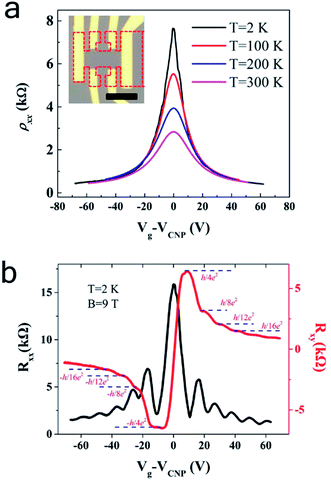
Electric transport measurement was conducted to investigate the electronic properties of the bilayer graphene structures obtained with this approach. We used Electron Beam Lithography (EBL) to fabricate bilayer graphene field effect transistor (FET) in a Hall bar geometry shown in Fig. 4a, after the post-oxidation bilayer graphene was transferred onto 300 nm oxide silicon wafer. Before electrodes (10 nm Ti and 40 nm Au) were deposited, the graphene sample was annealed in vacuum system to improve the contact between graphene and substrate. Fig. 4 illustrates the sheet resistance as a function of gate voltages measured under a vacuum of 10 Torr at temperature 2 K, 100 K, 200 K and 300 K. All four curves show typical ambipolar behavior of graphene FET devices, confirming the high quality of bilayer graphene prepared with this method. The mobility is determined to be μe = 3520 (μh = 3490) and μe = 3750 (μh = 3590) cm2 V−1 s−1 respectively at 300 K and 2 K, significantly higher than the reported RT value of ∼500 cm2 V−1 s−1 for LPCVD,3,28 and recent bilayer graphene in the range of 1400–4400,29 compared to defect-free mechanically exfoliated bilayer graphene.30 Here the carrier mobility was obtained by the equation μ = (1/Cg)∂σ/∂Vg, where σ = 1/ρxx is the sheet conductance and Cg = 1.15 × 10⁻¹⁸ F cm−2 is the back gate capacitance. Moreover, we investigated the Quantum Hall Effect (QHE) on the device to study the quality of the bilayer graphene. Fig. 4b plots the longitudinal resistance (Rxx) and Hall resistance (Rxy) as a function of the back gate voltage which was measured at 2 K with a perpendicular magnetic field B = 9 T. Pronounced plateaus can be clearly seen in the Hall resistance Rxy = ±h/4Ne2 with N ≥ 1, which are accompanied by the oscillations in the longitudinal resistance Rxx. The well-shaped and symmetric QHE indicates a high quality of our CVD bilayer graphene, comparable to the mechanically exfoliated bilayer graphene.31
Conclusions
In summary, here we developed a simple method to directly visualize bilayer graphene nucleus on the growth Cu substrate. With this method, we were able to visualize the structure of bilayer nucleus on copper by controlled oxidation in air. The key is that we utilize the lower oxidation resistance for monolayer graphene, which is further enhanced by the induced mechanical strain applied from the underneath oxidized Cu nanoparticles. On the other hand, the structure of bilayer graphene is less affected as confirmed by Raman and electronic transport measurement. The visualization technique reported here gives us a tool to fast observe the nucleation formation process in the chemical vapor deposition, and would enable fundamental study of graphene growth with controlled number of layers by providing statistically important information about graphene growth.Methods
Copper foil pretreatment
Here we use copper foil purchased from Alfa Aesar (Stock no. 13382) to synthesize graphene grains. Copper foil was cut into small size (around 2 cm × 8 cm) and then chemically polished with FeCl3 (5 g FeCl3, 10 mL HCl and 100 mL DI water) in ultrasonic for 10–15 seconds. After that, polished copper foil was rinsed with DI water for at least three times to remove residues. Finally, copper foil was blow-dried with nitrogen.Graphene synthesis by chemical vapor deposition
Polished copper foil was loaded into 1 inch diameter quartz tube and purge with 350 sccm high-purity argon gas for at least 20 minutes. The system temperature were then ramp to 1050 °C within 30 minutes, followed by charging with 15 sccm high-purity hydrogen and 15 sccm methane (500 ppm in Ar) and kept for 1 hour to grow large sized graphene grains.Graphene transfer
Graphene is transferred by electrochemical method, similar as previous report.32 1 M NaOH is used as electrolyte, while saturated calomel electrode and Pt are used as reference and counter electrodes, respectively.Characterizations
SEM was done using a JEOL 6390 scanning electron microscope operated at 20 keV. The Raman spectrum was recorded with a Renishaw Raman RM3000 scope using a 514 nm excitation argon laser. Mapping condition: 20× objectives lens, with 1.5 μm step in both X and Y axis. AFM was scanned under semi-contact mode using a NTEGRA probe NanoLaboratory (NT-MDT, Inc.) with ACTA tips from AppNano at 1.5 Hz scan rate and 512 × 512 resolutions. Optical images were taken by a LEICA DFC 290 optical microscope.Device fabrication and electronic measurement
Graphene layers, after being transferred onto the 300 nm oxide Si wafer, was first defined into the Hall bar geometry by using e-beam lithography (Raith e-LiNE, 10 kV) and then etched by oxygen plasma.33 Metal contacts were defined by a second e-beam lithography step followed by e-beam evaporation of 10 nm Ti and 40 nm Au. The contact resistance is usually on the order of several hundred Ohms. All the measurements were carried out in Physical Property Measurement System (PPMS, Quantum Design). Before measurement, graphene samples were heated in situ to 380 K in high vacuum for several hours to remove the adsorbed water molecules and PMMA residues. Electrical measurements were carried out by using a Keithley 6221 AC/DC source and a Keithley 2182A nanovoltmeter. Four-probe method was used during measurement to avoid contact resistance.Acknowledgements
This project is supported by the Research Grant Council of Hong Kong SAR of Project number 623512 and DAG12EG05, Grant no. SRFI11/SC02 and HKUST9/CRF/08. Technical assistance from the Materials Characterization and Preparation Facilities is greatly appreciated.References
- T. Ohta, A. Bostwick, T. Seyller, K. Horn and E. Rotenberg, Science, 2006, 313, 951–954 CrossRef CAS PubMed.
- L. X. Liu, H. L. Zhou, R. Cheng, W. J. Yu, Y. Liu, Y. Chen, J. Shaw, X. Zhong, Y. Huang and X. F. Duan, ACS Nano, 2012, 6, 8241–8249 CrossRef CAS PubMed.
- K. Yan, H. L. Peng, Y. Zhou, H. Li and Z. F. Liu, Nano Lett., 2011, 11, 1106–1110 CrossRef CAS PubMed.
- H. L. Zhou, W. J. Yu, L. X. Liu, R. Cheng, Y. Chen, X. Q. Huang, Y. Liu, Y. Wang, Y. Huang and X. F. Duan, Nat. Commun., 2013, 4, 2096 Search PubMed.
- L. Gan and Z. T. Luo, ACS Nano, 2013, 7, 9480–9488 CrossRef CAS PubMed.
- Y. F. Hao, M. S. Bharathi, L. Wang, Y. Y. Liu, H. Chen, S. Nie, X. H. Wang, H. Chou, C. Tan, B. Fallahazad, H. Ramanarayan, C. W. Magnuson, E. Tutuc, B. I. Yakobson, K. F. McCarty, Y. W. Zhang, P. Kim, J. Hone, L. Colombo and R. S. Ruoff, Science, 2013, 342, 720–723 CrossRef CAS PubMed.
- C. C. Jia, J. L. Jiang, L. Gan and X. F. Guo, Sci. Rep., 2012, 2, 707 Search PubMed.
- X. S. Li, W. W. Cai, J. H. An, S. Kim, J. Nah, D. X. Yang, R. Piner, A. Velamakanni, I. Jung, E. Tutuc, S. K. Banerjee, L. Colombo and R. S. Ruoff, Science, 2009, 324, 1312–1314 CrossRef CAS PubMed.
- K. S. Novoselov, A. K. Geim, S. V. Morozov, D. Jiang, Y. Zhang, S. V. Dubonos, I. V. Grigorieva and A. A. Firsov, Science, 2004, 306, 666–669 CrossRef CAS PubMed.
- P. Blake, E. W. Hill, A. H. C. Neto, K. S. Novoselov, D. Jiang, R. Yang, T. J. Booth and A. K. Geim, Appl. Phys. Lett., 2007, 91, 063124 CrossRef PubMed.
- X. C. Jiang, T. Herricks and Y. N. Xia, Nano Lett., 2002, 2, 1333–1338 CrossRef CAS.
- Y. C. Shin and J. Kong, Carbon, 2013, 59, 439–447 CrossRef CAS PubMed.
- J. S. Bunch, S. S. Verbridge, J. S. Alden, A. M. van der Zande, J. M. Parpia, H. G. Craighead and P. L. McEuen, Nano Lett., 2008, 8, 2458–2462 CrossRef CAS PubMed.
- P. Wu, X. F. Zhai, Z. Y. Li and J. L. Yang, J. Phys. Chem. C, 2014, 118, 6201–6206 CAS.
- G. H. Han, F. Gunes, J. J. Bae, E. S. Kim, S. J. Chae, H. J. Shin, J. Y. Choi, D. Pribat and Y. H. Lee, Nano Lett., 2011, 11, 4144–4148 CrossRef CAS PubMed.
- L. Gao, J. R. Guest and N. P. Guisinger, Nano Lett., 2010, 10, 3512–3516 CrossRef CAS PubMed.
- M. Schriver, W. Regan, W. J. Gannett, A. M. Zaniewski, M. F. Crommie and A. Zettl, ACS Nano, 2013, 7, 5763–5768 CrossRef CAS PubMed.
- K. Kim, S. Coh, L. Z. Tan, W. Regan, J. M. Yuk, E. Chatterjee, M. F. Crommie, M. L. Cohen, S. G. Louie and A. Zettl, Phys. Rev. Lett., 2012, 108, 246103 CrossRef.
- J. S. Hwang, Y. H. Lin, J. Y. Hwang, R. L. Chang, S. Chattopadhyay, C. J. Chen, P. L. Chen, H. P. Chiang, T. R. Tsai, L. C. Chen and K. H. Chen, Nanotechnology, 2013, 24, 015702 CrossRef PubMed.
- R. Rao, R. Podila, R. Tsuchikawa, J. Katoch, D. Tishler, A. M. Rao and M. Ishigami, ACS Nano, 2011, 5, 1594–1599 CrossRef CAS PubMed.
- L. Liu, S. M. Ryu, M. R. Tomasik, E. Stolyarova, N. Jung, M. S. Hybertsen, M. L. Steigerwald, L. E. Brus and G. W. Flynn, Nano Lett., 2008, 8, 1965–1970 CrossRef CAS PubMed.
- M. Yamamoto, T. L. Einstein, M. S. Fuhrer and W. G. Cullen, ACS Nano, 2012, 6, 8335–8341 CrossRef CAS PubMed.
- D. Srivastava, D. W. Brenner, J. D. Schall, K. D. Ausman, M. F. Yu and R. S. Ruoff, J. Phys. Chem. B, 1999, 103, 4330–4337 CrossRef CAS.
- S. Park, D. Srivastava and K. Cho, Nano Lett., 2003, 3, 1273–1277 CrossRef CAS.
- I. Wlasny, P. Dabrowski, M. Rogala, P. J. Kowalczyk, I. Pasternak, W. Strupinski, J. M. Baranowski and Z. Klusek, Appl. Phys. Lett., 2013, 102, 111601 CrossRef PubMed.
- Q. Wang, L. Wei, M. Sullivan, S.-W. Yang and Y. Chen, RSC Adv., 2013, 3, 3046 RSC.
- Y. H. Zhang, B. Wang, H. R. Zhang, Z. Y. Chen, Y. Q. Zhang, Y. P. Sui, X. L. Li, X. M. Xie, G. H. Yu, Z. Jin and X. Y. Liu, Carbon, 2014, 70, 81–86 CrossRef CAS PubMed.
- S. Lee, K. Lee and Z. H. Zhong, Nano Lett., 2010, 10, 4702–4707 CrossRef CAS PubMed.
- L. Liu, H. Zhou, R. Cheng, W. J. Yu, Y. Liu, Y. Chen, J. Shaw, X. Zhong, Y. Huang and X. Duan, ACS Nano, 2012, 6, 8241–8249 CrossRef CAS PubMed.
- K. Zou and J. Zhu, Phys. Rev. B: Condens. Matter Mater. Phys., 2010, 82, 081407 CrossRef.
- K. S. Novoselov, E. McCann, S. V. Morozov, V. I. Fal'ko, M. I. Katsnelson, U. Zeitler, D. Jiang, F. Schedin and A. K. Geim, Nat. Phys., 2006, 2, 177–180 CrossRef.
- L. B. Gao, W. C. Ren, H. L. Xu, L. Jin, Z. X. Wang, T. Ma, L. P. Ma, Z. Y. Zhang, Q. Fu, L. M. Peng, X. H. Bao and H. M. Cheng, Nat. Commun., 2012, 3, 699 CrossRef PubMed.
- H. Zhang, J. Lu, W. Shi, Z. Wang, T. Zhang, M. Sun, Y. Zheng, Q. Chen, N. Wang, J.-J. Lin and P. Sheng, Phys. Rev. Lett., 2013, 110, 066805 CrossRef.
Footnotes |
| † Electronic supplementary information (ESI) available. See DOI: 10.1039/c5ra00865d |
| ‡ These authors contributed equally to this work. |
| This journal is © The Royal Society of Chemistry 2015 |


