Nanostructured PEDOT:PSS film with two-dimensional photonic quasi crystals for efficient white OLED devices
Massimo
Rippa†
a,
Rossella
Capasso
a,
Lucia
Petti
*a,
Giuseppe
Nenna†
b,
Anna
De Girolamo Del Mauro
b,
Maria Grazia
Maglione
b and
Carla
Minarini
b
aInstitute of Cybernetics “E. Caianiello” of CNR,
Via Campi Flegrei 34, 80072 Pozzuoli, Italy. E-mail: L.petti@cib.na.cnr.it
bUTTP ENEA Portici Research Centre, Piazza E. Fermi 1, 80055 Portici, Italy. E-mail: giuseppe.nenna@enea.it
First published on 28th October 2014
Abstract
A polymeric PEDOT:PSS film nanostructured with Photonic Quasi Crystals that opens the path towards more efficient white OLEDs is presented. For the first time three different quasi crystal families were fabricated (octagonal, dodecagonal and Thue-Morse) onto a conductive polymeric film combining high-resolution electron beam lithography (EBL) and plasma etching techniques to improve light extraction and to control spectral tunability. The efficiency gain obtained in light extraction holds great promise for the use of quasi crystals as functional components in polymeric based White Organic Light Emitting Diode (WOLED) devices.
Introduction
WOLED (White Organic Light Emitting Diode) devices are attracting much attention from researchers all over the world because of their possible use in optoelectronics and in particular in lighting technology.1,2 The improvements in terms of their external quantum efficiency (EQE) in recent years have been tremendous but still a lot can be done to ensure a key role for this class of devices to save energy. In particular, the use of innovative optical structures such as microlenses, photonic crystals, diffusive films, and optical cavities can considerably reduce optical losses due to optical waveguide effects that usually affect multilayered devices.3–6 All these approaches are usually utilized on devices with a single narrow emission band because of their effect on the spectral emission and the consequent change of the CIE (Commission Internationale de l'Eclairage) diagram.As it is well known, organic LEDs have wide band emission and this is even more evident in white-emitting OLEDs in which there is usually more than one light emitting band. Lately, in order to tune the emission properties of the polymer within the CIE framework and to improve the device lifetime, it was useful to combine emitting polymers and luminescent dyes, i.e. quantum dots7 and small molecules.8 Polyfluorenes and oxadiazole–carbazole derivatives were widely used as the polymeric active matrix because of their strong blue emission.9,10
On the other hand, photonic quasi-crystals can be employed to help change the spectral emissions and to improve the efficiency in one or more spectral bands, thus, to contribute to designing innovative WOLED architectures. Several tiling geometries have been considered based on different ways of structuring the photonic crystal and engineering its band gap properties in view of its use as a practical solid-state light-emitting source.11–13 Recent studies14–16 on photonic quasicrystals (PQCs) with 8-fold (octagonal point group), 10-fold (decagonal), and 12-fold (dodecagonal) rotational symmetries have shown that, in general, higher order rotational symmetry results in an increase of the density of points in the reciprocal space which is important for designing efficient omni-directional outcouplers. Recently, a 12-fold PQC pattern was used to improve the efficiency of light extraction of polymer light-emitting diodes (PLEDs).17
In previous studies PQC patterns were also directly realized on the anodic electrode to simplify the PQC–OLED architecture. In particular, the ITO electrode was partially patterned by focused ion beam (FIB) covered by PEDOT:PSS achieving a good efficiency increase18 and the low refractive index of PEDOT:PSS19 gives a high refractive index jump for the ITO-PEDOT:PSS structure that is advantageous also on microstructured20 or nanostructured grids.21 Recently, an ITO-free electrode structure has been integrated into an OLED device utilizing the combination of EBL and PE techniques to fabricate a novel polymeric anode structure based on 2D nanopatterned conductive PEDOT:PSS layers.22
In this work, to the best of our knowledge, this is the first time that photonic quasi crystal patterns are realized directly on dimethylsulfoxide (DMSO) doped PEDOT:PSS polymeric films, and that PQC properties are deeply explored to investigate their potential applications in white OLED devices. Three different PQC families (octagonal, dodecagonal and Thue-Morse patterns)23–25 are compared to control the spectral emissions and enhance the lighting efficiency of WOLED devices.
Results and discussion
Photonic quasi crystals
Photonic quasi crystals26–30 are a class of structures that do not have translational symmetry, but obey local rotational symmetry, very often with symmetry axes forbidden for regular crystals, e.g., five-fold rotational symmetry. Originally discovered for rapidly annealed metallic alloys by Shechtman,26 photonic quasi crystals are man-made structures. As quasi crystals combine both long-range order as in photonic crystals (although not in a repeating fashion) and local arrangements of atoms in fixed positions but with different configurations of the surrounding atoms like in glasses, they promise to possess unusual optical transport properties. The structural complexity of PQCs is measured by their spatial Fourier spectra, which are discrete (singular) for quasiperiodic systems, singular-continuous, or absolutely continuous for pseudorandom structures of increasing complexity.The Thue-Morse (TM) sequence is an example of an aperiodic structure with a singular continuous contribution to the diffraction pattern. To construct the 2-D TM structure, a one-dimensional binary TM sequence is firstly constructed using the following rule. First of all, let us give an arbitrary sequence of two symbols, A = 0 and B = 1, and then a new sequence is formed by replacing each occurrence of A with the pair (A, B) and each occurrence of B with the pair (B, A).31 This sequence is neither periodic nor quasiperiodic. By inflation rules the one-dimensional aperiodic lattice can be generalized to the two-dimensional space introducing a substitutional matrix obtained as the Cartesian product of 1D TM sequences.25,32,33
In this work, 2D TM structures have been experimentally obtained by removing particular lattice points from a regular square array with lattice constant a by EBL as described in the Experimental section. The selected units are chosen in agreement with the inflation rules encoded into the substitutional matrix of the 2D TM sequence. The centres of the air filled rods were located at the vertices of a 2D TM lattice of order N = 10.
The fabricated octagonal structure was determined by simulating the quasi periodic transverse irradiance distribution given by the 8-beam interference process and was theoretically analyzed through finite difference time domain (FDTD) simulations of the transmittance spectra.34
The 12-fold quasicrystal structure proposed by Zoorob in 2000 grown by the use of the random Stampfly inflation method is based on a dodecagon composed of an inner hexagon consisting of six equilateral triangles surrounded by a ring of squares and equilateral triangles. Our structure is a “triangle–triangle” crystal configuration with a rod radius to pitch length ratio (r/a) of 0.25.
Nanopatterned PEDOT:PSS film fabrication
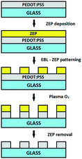
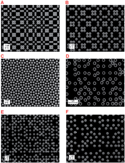
Our method to directly pattern the highly conductive22 PEDOT:PSS films together with the whole fabrication process is described in Fig. 1. PEDOT:PSS-quasi periodic nanostructured arrays were fabricated by electron-beam lithography (EBL) on glass substrates. The realized two-dimensional photonic quasi crystals are made of air rods embedded into the organic matrix of a styrene methyl acrylate based polymer (ZEP) with lattice parameters calculated with numerical simulations.Such nanostructured ZEP films were used as a lithographic mask during the anisotropic plasma etching process. Through this process, six PQC nanostructures were realized using the following arrangements: (A) octagonal, (B) dodecagonal, and (C) Thue-Morse of order M = 10.
In particular the fabricated structures are: octagonal patterns with air rods of diameters d = 250 nm, d = 500 nm and d = 750 nm, a dodecagonal pattern with air rods of diameter d = 500 nm and lattice constant a = 1000 nm, and Thue-Morse patterns of order M = 10 with air rods of diameters d = 500 nm and d = 750 nm and lattice constants a = 720 nm and a = 1080 nm respectively.
White polymer fabrication
In order to establish the contribution of the PQC structures to white OLED devices we prepared organic white-light-emitting blend materials and then spinned them on the nanostructured anodes. These polymers were selected also because they have already been used in polymer light emitting diodes.35 Initially, thin films (∼70 nm) with different concentrations of poly[2-methoxy-5-(3′,7′-dimethyloctyloxy)-1,4-phenylenevinylene] (MDMO-PPV) in a polyfluorene oxadiazole (PFO) polymer were prepared by spin-coating on glass substrates in order to optimize the concentration of MDMO-PPV to obtain white emission. It was observed that the optimal concentration to obtain white emission is with 2 wt% of MDMO-PPV in a PFO polymer. Fig. 2 shows the photoluminescence intensity of films containing PFO and PFO with 2 wt% of MDMO-PPV.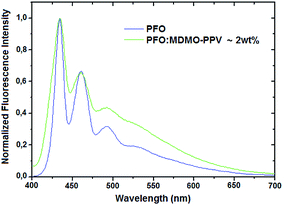 | ||
| Fig. 2 Fluorescence spectra of pure PFO (blue curve), and PFO:MDMO-PPV (green curve) films with an excitation at 380 nm. | ||
Morphological and optical characterization
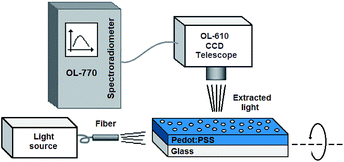
The PQC polymeric nanostructures realized were characterized in the direct space through metrological measurements by scanning electron microscopy (SEM) (Fig. 3).An optical set-up was adopted to evaluate the PQC properties at room temperature and to have an estimation about the extracted spectrum36,37 of the different lattices which better matches the desired properties of the final OLED. The set-up to measure the light propagating in the glass substrate which is extracted by diffraction is reported in Fig. 4. The PQC-based polymeric structures were tested introducing white light from the edge of the glass substrate that propagated inside the glass due to total internal reflection phenomena.
Study of light extraction
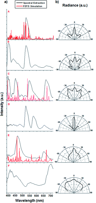
The vertical extracted spectra (0 degree) of the nanostructured films are shown in Fig. 5a. All the spectra have an extracted background into the whole visible region and different extraction bands can be distinguished in the analyzed signal for all the samples realized. The full width half maximum was mainly between 30 and 50 nm for each band observed. Fig. 5b shows the radial properties of the emission pattern for the different PQCs. Lattice symmetry not only has an important effect on extraction efficiency and beam directionality but also on the quality of the far field emission pattern.In order to achieve the enhancement of out-coupling efficiency through an appropriate chip design, we performed the calculation of the resonant frequencies for a single pattern belonging to each family of the quasi-crystals considered by 3D numerical simulations (red line in Fig. 5a). The results obtained have provided indications concerning the possibility to get extracted peaks in the visible region. We employed a finite difference time-domain numerical method (FDTD) performed with a commercial software (Full Wave simulation tool, RSoft Design Group, Ossining, NY). We have assumed that the glass substrate (corning eagle 2000) and air are semi-infinite with constant refractive indices nglass = 1.51 and nair = 1, whereas the dispersion relationship in the spectral region of interest has been used for the PEDOT:PSS film. The thickness of the polymer and depth of the holes used is tpedot:pss = tholes = 160 nm. During the calculations, we used a time step (in units of ct) of 10–2 μm and a spatial grid with a step size of 20 nm for each direction. Periodic boundary conditions on the x–z plane of the nanostructure and perfectly matched layer (PML) boundary conditions on the y direction were used for the dodecagonal and Thue-Morse structures while PML conditions were used in all directions for the octagonal structure, since it is difficult to design a periodic cell on this kind of pattern. In particular, we used a rhombic unit supercell for the dodecagonal pattern and an M4 order supercell for the Thue-Morse pattern.31 The simulated structures were excited from air by a short impulse with a broad spectrum and plane wavefront. It can be noticed that the experimental resonances exhibit a good match with the simulated peaks.
Starting from the simulated data, we scaled octagonal and Thue-Morse patterns in order to have more and different extracted bands in the region of interest. In particular, for the Thue-Morse structure we increased the size of the holes trying to obtain more peaks in the visible region, while, referring to the octagonal structure, we have both increased and decreased the hole size to evaluate the displacement of the two peaks highlighted by the first structure realized.
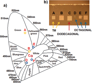
The dodecagonal pattern shows many extracted pathways with the selected lattice parameters. Fig. 5b shows how the geometrical parameters affect both the extracted spectra and the angular radiance profiles. In particular, the background of the extracted light increases as the sizes of the pattern increase and make the structure more diffusive with a more isotropic angular profile extraction. Moreover, the CIE diagram (Fig. 6a), associated with A, C and E spectra in Fig. 5a, shows that the dodecagonal photonic structure has an extracted spectrum well localized in the white region, close to x = 0.33 and y = 0.33 coordinates, while the octagonal and the Thue-Morse nanostructures could be further optimized.
Fig. 6a shows the spectrally integrated light intensity characteristics related to all the realized structures and gives us the opportunity to select the appropriate structures to be used to enhance efficiency in a white OLED device. In this regard, it is possible to observe that the structures B (Thue-Morse d = 500 nm, a = 1080 nm), C (dodecagonal) and F (octagonal, d = 750 nm) are closer to the white point.
The image in Fig. 6b obtained with an optical microscope shows the extracted light by PQC areas while white light propagates into the glass substrate. The PQC areas were seen almost white for all the fabricated structures because of the wavelength-selective diffraction by the quasi-periodic nanopatterns. In the case of white sources, to achieve a large enhancement of light extraction, it is important to explore all the physical parameters that modify the light propagation via diffraction on nanometric patterns and relate them to the emission bands of the white source. The experimental results demonstrate that the realized photonic structures are then perfectly transferred onto the PEDOT:PSS films and that our method may offer the possibility to exploit a large variety of new functionalities of the innovative nanostructures.
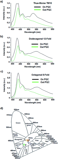
We repeated the experiment on the structures B, C and F after covering them with the organic white-light-emitting blend material (PFO/MDMO-PPV) by the spin coating process.
We used a UV LED as the light probe (wavelength peak 360 nm) to stimulate the fluorescence of the polymer. We analyzed the fluorescence spectra coming from the nanostructured areas (straight lines, Fig. 7) and from the nearby non-structured areas (dot lines, Fig. 7). In this way we can predict the enhancement resulting from the use of PQC structures in combination with an emitting polymer that might be used in WOLED stacked devices. In particular, we observed an enhancement in the light extracted of 55%, 66% and 68% related to the octagonal, Thue-Morse and dodecagonal structures, respectively, calculated by the formula [(RoutPQC − RinPQC)/RinPQC] × 100, where R is the measured spectral radiance.
It is worthwhile noting that with the use of the proposed architectures for a WOLED device it is also very important to achieve holes in the designed patterns of depth that do not affect the electrical continuity, thus avoiding reaching the glass.38 Moreover, the radiation emitted by the device is further affected by the presence of the cathode.39
In summary, we demonstrated the possibility to realize a PQC directly on the polymeric film surface combining EBL and a Plasma Etching (PE) process to partially structure PEDOT:PSS. We performed several measurements and simulations to elude the trial and error approach and to investigate the quasi-photonic structures according to the fluorescence spectra of the emitter polymer, to easily achieve a real enhancement of light extraction. Thus this kind of characterization allows us to compare and evaluate the enhancement of the extracted light in different quasi periodic/deterministic aperiodic patterns in white OLED applications without necessarily producing a great number of test devices.
Experimental section
Nanopatterned organic film fabrication
Our method to directly pattern the organic films together with the whole fabrication process is described in Fig. 1. PEDOT:PSS-quasi periodic nanostructured arrays were fabricated by electron-beam lithography (EBL) on glass substrates. Highly conductive PEDOT:PSS (160 nm) was spin coated onto a corning glass substrate. Such a highly conductive film was obtained by doping the PEDOT:PSS with DMSO as described in a previous paper.40 Then, a 200 nm thick layer of a styrene methyl acrylate based polymer (ZEP), which is electron-sensitive, was spin-coated on top of the cleaned PEDOT-PSS surfaces. Thereafter, the resulting films were dried in an oven at 170 °C for 5 min. An e-beam direct writing system (Raith150) was used to define the pattern operating at 10 keV with an electron dosage of 24 pA. Finally, nanostructured arrays were formed after developing in n-amyl acetate for two minutes. Such nanostructured ZEP films were used as a lithographic mask during the anisotropic plasma etching process performed using a high-vacuum Plasma Enhanced Chemical Vapor Deposition (PECVD) system (Plasmalab800+, Oxford Inst.) operating at 13.56 MHz with these parameters: power density around 270 mW cm−2, 200 sccm for O2, and pressure 400 mTorr for 10 minutes of treatment at 100 °C. As the final step, the anisole solvent was used to remove the ZEP without damaging the underlying PEDOT:PSS film.Functionalization of nanostructures with the white polymer
Organic white-light-emitting blend materials were prepared by mixing PFO and MDMO-PPV as the blue host and the red guest emitting materials, respectively. PFO was dissolved in chlorobenzene with a material content of 15 mg ml−1 and MDMO-PPV was added at various concentrations (1, 2 and 5 wt%) in the same solvent.PFO films with 2 wt% of MDMO-PPV were deposited by spin coating on the nanopatterned DMSO-PEDOT:PSS substrates. These films were then annealed at 120 °C in an oven for 2 hours.
Measurement set-up
The nanostructured substrates have been characterized by Scanning Electron Microscopy and out-of-plane diffraction measurements. The set-up to measure the light propagating in the glass substrate which is extracted by diffraction (Fig. 4) is composed of a multimode fiber, a CCD imaging telescope (OL610), and a CCD-based spectroradiometer (OL770-LED). The sample is placed on a rotating holder which allows the angular resolved measurements. The PQC-based polymeric structures were tested introducing white light from the edge of the glass substrate that propagated inside the glass due to total internal reflection phenomena.Conclusions
In conclusion, we have demonstrated PQC polymeric film properties experimentally and numerically. As a result, spectral modifications and emission enhancement of polymeric WOLED based devices can be optimized with the present study. We demonstrated that the PQCs can be designed to match the properties of the active photonic material by changing both the arrangement and the geometrical parameters of the structures to obtain, eventually, enhanced performances of the PQC based device. We simulated and then selected three different arrangements of photonic quasi-crystals exhibiting a good enhancement in light extraction in the wavelength range overlapping the photoluminescence emission of the fluorescent polymeric layer. Finally, it has been shown that using PQC nanostructures in a highly conductive PEDOT:PSS polymeric film a remarkable efficiency gain is obtained with an improvement higher than 60% for white light emission.Acknowledgements
This work has been financially supported by the Italian Ministry of Education, University and Research (MIUR) through the National Project entitled Relight (PN: PON02 00556 3306937).Notes and references
- W. Mróz, C. Botta, U. Giovanella, E. Rossi, A. Colombo, C. Dragonetti, D. Roberto, R. Ugo, A. Valore and J. A. G. Williams, J. Mater. Chem., 2011, 21, 8653 RSC.
- L. Murphy, P. Brulatti, V. Fattori, M. Cocchi and J. A. G. Williams, Chem. Commun., 2012, 48, 5817 RSC.
- S. Moller and S. R. Forrest, J. Appl. Phys., 2002, 91, 3324 CrossRef CAS PubMed.
- G. Nenna, A. De Girolamo Del Mauro, E. Massera, A. Bruno, T. Fasolino and C. Minarini, J. Nanomater., 2012, 319398 Search PubMed.
- Y. J. Lee, S.-H. Kim, J. Huh, G.-H. Kim, Y.-H. Lee, S.-H. Cho, Y.-C. Kim and Y. Rag Do, Appl. Phys. Lett., 2003, 82, 3779 CrossRef CAS PubMed.
- W. Li, R. A. Jones, S. C. Allen, J. C. Heikenfeld and A. J. Steck, J. Disp. Technol., 2006, 2, 143 CrossRef CAS.
- S. Coe-Sullivan, W. K. Woo, J. S. Steckel, M. Bawendi and V. Bulovic, Org. Electron., 2003, 4, 123 CrossRef CAS PubMed.
- B. W. D'Andrade, M. E. Thompson and S. R. Forrest, Adv. Mater., 2002, 14, 147 CrossRef.
- H. Wanga, Y. Xua, T. Tsuboi, H. Xua, Y. Wua, Z. Zhanga, Y. Miaoa, Y. Haoa, X. Liua, B. Xua and W. Huang, Org. Electron., 2013, 14, 827 CrossRef PubMed.
- S. Concilio, V. Bugatti, P. Iannelli and S. Piotto, Int. J. Polym. Sci., 2010, 2010, 581056 Search PubMed.
- A. David, H. Benisty and C. Weisbuch, J. Disp. Technol., 2007, 3, 2 CrossRef.
- A. David, T. Fujii, E. Matioli, R. Sharma, S. Nakamura, S. P. DenBaars, C. Weisbuch and H. Benisty, Appl. Phys. Lett., 2006, 88, 073510 CrossRef PubMed.
- A. David, H. Benisty and C. Weisbuch, Rep. Prog. Phys., 2012, 75, 126501 CrossRef PubMed.
- M. Florescu, S. Torquato and P. J. Steinhardt, Phys. Rev. B: Condens. Matter Mater. Phys., 2009, 80, 1551121 CrossRef.
- D. N. Chigrin and A. V. Lavrinenko, in Metamaterials Handbook, ed. F. Capolino, Boca Raton, Fl, USA, 2004, ch. 28 Search PubMed.
- X. Zhang, Z.-Q. Zhang and C. T. Chan, Phys. Rev. B: Condens. Matter Mater. Phys., 2001, 63, 081105 CrossRef.
- J. H. Lin, W. L. Chang, H.-Y. Lin, T.-H. Chou, H.-C. Kan and C. Chen, Opt. Express, 2013, 21, 22090 CrossRef PubMed.
- C. Tsai, L. Liao, Y. Luo, P. C. Chao, E. Chen, H. Meng, W. Chen, S. Lin and C. Lin, Microelectron. Eng., 2010, 87, 1331 CrossRef CAS PubMed.
- D. Zhu, W. Shen, H. Ye, X. Liu and H. Zhen, J. Phys. D: Appl. Phys., 2008, 41, 235104 CrossRef.
- T.-W. Koh, J.-M. Choi, S. Lee and S. Yoo, Adv. Mater., 2010, 22, 1849 CrossRef CAS PubMed.
- L. Petti, M. Rippa, R. Capasso, G. Nenna, A. De Girolamo Del Mauro, V. La Ferrara, A. P. Madathil and C. Minarini, JEOS-RP, 2013, 8, 13002 CrossRef.
- L. Petti, M. Rippa, R. Capasso, G. Nenna, A. De Girolomo Del Mauro, G. Pandolfi, M. Maglione and C. Minarini, ACS Appl. Mater. Interfaces, 2013, 5, 4777 CAS.
- L. Petti, M. Rippa, J. Zhou, L. Manna, M. Zanella and P. Mormile, Nanoscale Res. Lett., 2011, 6(371), 1 Search PubMed.
- M. Rippa, R. Capasso, P. Mormile, S. De Nicola, M. Zanella, L. Manna, G. Nenna and L. Petti, Nanoscale, 2013, 5, 331 RSC.
- M. Rippa, S. De Nicola, R. Capasso, P. Mormile, J. Zhou and L. Petti, Sci. Adv. Mater., 2014, 6, 320 CrossRef CAS PubMed.
- D. Shechtman, I. Blech, D. Gratias and J. W. Cahn, Phys. Rev. Lett., 1984, 53, 1951 CrossRef CAS.
- D. Levine, T. C. Lubensky, S. Ostlund, S. Ramaswamy, P. J. Steinhardt and J. Toner, Phys. Rev. Lett., 1985, 54, 1520 CrossRef CAS.
- P. J. Steinhardt and S. Ostlund, The Physics of Quasicrystals, World Scientific, Singapore, 1987 Search PubMed.
- C. Janot, Quasicrystals, Clarendon Press, Oxford, 1992 Search PubMed.
- L. Bindi, P. J. Steinhardt, N. Yao and P. J. Lu, Science, 2009, 324, 1306 CrossRef CAS PubMed.
- L. Moretti and V. Mocella, Opt. Express, 2007, 15, 15314 CrossRef.
- V. Matarazzo, S. De Nicola, G. Zito, P. Mormile, M. Rippa, G. Abbate, J. Zhou and L. Petti, J. Opt., 2011, 13, 015602 CrossRef.
- Y. Ming-yang, J. Zhou, L. Petti, S. De Nicola and P. Mormile, Optoelectronics Letters, 2011, 7 Search PubMed.
- L. Petti, V. Matarazzo, M. Rippa, G. Zito, S. De Nicola, G. Abbate and P. Mormile, AIP Conf. Proc., 2009, 1176, 146 CrossRef CAS PubMed.
- R. Bauer, W. J. Finkenzeller, U. Bogner, M. E. Thompson and H. Yersin, Org. Electron., 2008, 9, 641 CrossRef CAS PubMed.
- A. David, H. Benisty and C. Weisbuch, Rep. Prog. Phys., 2012, 75, 126501 CrossRef PubMed.
- A. David, T. Fujii, R. Sharma, K. McGroddy, S. Nakamura, S. P. DenBaars, E. L. Hu, C. Weisbuch and H. Benisty, Appl. Phys. Lett., 2006, 88, 061124 CrossRef PubMed.
- A. O. Altun, S. Jeon, J. Shim, J.-H. Jeong, D.-G. Choi, K.-D. Kim, J.-H. Choi, S.-W. Lee, E.-S. Lee, H.-D. Park, J. R. Youn, J.-J. Kim, Y.-H. Lee and J.-W. Kang, Org. Electron., 2010, 11, 711 CrossRef CAS PubMed.
- L. Petti, M. Rippa, R. Capasso, G. Nenna, A. De Girolamo Del Mauro, M. Maglione and C. Minarini, Nanotechnology, 2013, 24, 315206 CrossRef PubMed.
- A. De Girolamo Del Mauro, G. Nenna, F. Villani and C. Minarini, Thin Solid Films, 2012, 520, 5386 CrossRef CAS PubMed.
Footnote |
| † These authors contributed equally to this work. |
| This journal is © The Royal Society of Chemistry 2015 |

