
Interface modification strategy based on a hybrid cathode buffer layer for promoting the performance of polymer solar cells†
Feng Yeabc,
Zhaobin Chenb,
Xiaoli Zhaoa,
Zidong Liabc and
Xiaoniu Yang*a
aState Key Laboratory of Polymer Physics and Chemistry, Changchun Institute of Applied Chemistry, Chinese Academy of Sciences, 5625 Renmin Street, Changchun 130022, P. R. China. E-mail: xnyang@ciac.jl.cn; Fax: +86-0431-85262028; Tel: +86-0431-85262206
bPolymer Composites Engineering Laboratory, Changchun Institute of Applied Chemistry, Chinese Academy of Sciences, 5625 Renmin Street, Changchun 130022, P. R. China
cUniversity of Chinese Academy of Sciences, 19 Yuquan Road, Shijingshan District, Beijing 100049, P. R. China
First published on 17th December 2015
Abstract
An interface modification strategy based on a hybrid cathode buffer layer (HCBL) is proposed and demonstrated through blending the interface modifier (4-fluoro-1,2-phenylenediamine, FPDA) with the host material (poly[(9,9-dioctyl-2,7-fluorene)-alt-(9,9-bis(3′-(N,N-dimethylamino)propyl)-2,7-fluorene)], PFN). By introducing FPDA, the carrier generation and extraction processes are regulated through the inhibition of interface exciton quenching, enhancement of hole blocking and passivation of electron transport, which are elaborated through steady-state and transient fluorescence spectra, frequency and bias related impedance analysis, and current density–voltage response. It is found that these three factors change simultaneously with the variation of FPDA content in HCBL, and the trade-off between the first two positive factors and the last one negative factor determines the final device performance. For instance, when the FPDA![[thin space (1/6-em)]](https://www.rsc.org/images/entities/char_2009.gif) :PFN weight ratio is 0.16, the power conversion efficiency of the device increases to 6.24%, which is promoted by almost 20% in comparison with 5.22% of the pristine device. Thanks to the effectiveness, controllability and processability, this interface modification strategy offers a general method to provide an electrode buffer layer with multiple functions and a device with improved performance.
:PFN weight ratio is 0.16, the power conversion efficiency of the device increases to 6.24%, which is promoted by almost 20% in comparison with 5.22% of the pristine device. Thanks to the effectiveness, controllability and processability, this interface modification strategy offers a general method to provide an electrode buffer layer with multiple functions and a device with improved performance.
1. Introduction
Polymer solar cells have been seen as potential options for sustainable energy sources due to their flexibility and solution-processing compatibility, and thus offer the prospect of reducing the costs of large-scale production.1–3 In the popular bulk heterojunction devices, the electrodes are in contact with both donor and acceptor components, leading to the necessity of inserting buffer layers with suitable charge selectivity for the respective carrier extraction.4–6The carrier selectivity of an electrode buffer layer is usually achieved through the interface charge redistribution upon the contact establishment and subsequent Fermi level alignment.7–9 However, achieving a desired electrical contact is still somewhat not easy due to the influence of the defective interface states in real case, which brings about the uncertainty of interface charge distribution.10–13 It is well known that the interface states, which are derived from the factors such as chemical bond formation, structural imperfection, thermal damage and diffusion phenomena, locate in the band gap, and the defective ones not only disrupt the energy level configuration for smooth charge transport, but also facilitate energy dissipation by over-consuming the excitons and carriers.14–16 For example, the interface states may provide excitons with quenching centers or charge carriers with recombination sites.17,18 Furthermore, when the density of interface states reaches a certain level, the consequent interface charge accumulation and energy band bending would dominate the electrical contact quality by screening the bulk properties, which is also called “Fermi level pinning”.19–21 In some cases, these non-regulated natures of the interface could hinder the effectiveness obtained by the energy level matching method for desired electrical contact properties.
Although the approach towards the mitigation of energy band disturbances from the aspect of interface states is still challenging,22–25 the introduction of surface modifiers has been proved to be effective in the modification of conductor work function.26 For example, the small molecules containing amine structure have exhibited the ability to reduce the electrode surface work function with significant effectiveness.27–29 For more complicated case of electrode buffer layer regulation, however, it is expected to obtain a variety of functions for device performance improvement.30,31 For cathode buffer layer, the interface states that may hinder the formation of hole-blocking barrier are presumed to be the trap states at the active layer donor surface, which would accommodate electrons and shift the donor energy band upward, thus inhibit the formation of thicker depletion region. From this point of view, the key to optimizing the cathode buffer layer is to exclude the impact of the interface states on the charge distribution while maintain the charge selectivity for electron conducting and hole blocking. However, using a single material to achieve such multiple purposes is difficult in controlling the buffer layer regulation and results in limited efficacy.
In this study, a strategy of hybridizing cathode buffer layer is proposed, in which the Lewis base of 4-fluoro-1,2-phenylenediamine (FPDA) is selected as the interface modifier and blended with the host material of poly[(9,9-dioctyl-2,7-fluorene)-alt-(9,9-bis(3′-(N,N-dimethylamino)propyl)-2,7-fluorene)] (PFN) to form the hybrid cathode buffer layer (HCBL). The HCBL exhibits systematic constituent-related natures including inhibition of interface exciton quenching, enhancement of hole-blocking ability and the passivation of electron transport capability, which have direct impacts on the carrier generation and extraction process. Among them, the first two factors are favorable while the later one should be avoided for the effective carrier extraction. The power conversion efficiency (PCE) of the photovoltaic devices containing HCBL is dominated by the combined contribution of these three factors, which is promoted in a wide range of FPDA content (<0.2 of FPDA:PFN weight ratio) and reaches 6.24% of the highest value for the device with HCBL containing 0.16 of FPDA:PFN weight ratio (20% increase in comparison with 5.22% of the pristine device without FPDA).
2. Experimental
2.1. Materials
Poly{4,8-bis(2′-ethylhexyloxy)-benzo[1,2-b:4,5-b′]-dithiophene-alt-[5,8-bis(5′-thiophen-2′-yl)-6,7-difluoro-2,3-bis-(3′′-hexyloxyphenyl)quinoxaline]} (PBDT-TFQ) (Mn = 35 kg mol−1, PDI = 2.0) and 4-fluoro-1,2-phenylenediamine (FPDA) were synthesized according to the previous literatures.32,33 1,8-Diiodooctane (DIO), chlorobenzene (CB, anhydrous, 99%) and o-dichlorobenzene (ODCB, anhydrous, 99%) were purchased from Sigma-Aldrich. MoO3 (99.9995%) and silver (99.999%) were obtained from Alfa Aesar. PC71BM (99.0%) and poly[(9,9-dioctyl-2,7-fluorene)-alt-(9,9-bis(3′-(N,N-dimethylamino)propyl)-2,7-fluorene)] (PFN) were acquired from American Dye Source Inc. and Derthon Optoelectronic Materials Co., Ltd., respectively. All materials were used as received.2.2. Device fabrication
PBDT-TFQ and PC71BM were dissolved in ODCB in the weight ratios of 1:1 with PBDT-TFQ concentration of 10 mg mL−1, and 3% volume fraction of DIO was added as the additive prior to the spin-coating process. Patterned indium tin oxide (ITO) coated glass substrate with sheet resistance of 10 Ω per square was cleaned in ultrasonic bath with deionized water, acetone and isopropanol alcohol for 20 min each and dried with nitrogen flow. The pre-cleaned substrate was treated in UV-ozone for 20 min and then transferred into a glove box with nitrogen atmosphere, after which the 5 nm thick HCBL was accomplished through spin coating FPDA:PFN blend film from chlorobenzene solution with 1 mg mL−1 of constant PFN concentration and varied FPDA content (represented by FPDA:PFN weight ratio). Afterwards, a 100 nm thick PBDT-TFQ:PC71BM (1:1, w/w) blend film was spin coated followed by a 10 min annealing treatment at 150 °C. The anode buffer layer of a 10 nm thick MoO3 layer and a 100 nm silver electrode layer were deposited sequentially under vacuum of ca. 5 × 10⁻⁴ Pa. The active area of each square device was 0.09 cm2. For the electron only device, a 30 nm thick calcium layer and a 100 nm aluminum electrode layer were thermally deposited under the same condition instead of MoO3 and silver.
2.3. Characterization
UV-Vis absorption spectra were recorded on a Lambda 750 spectrometer (Perkin-Elmer, Wellesley, MA).Cyclic voltammetry was conducted on a CHI instrument (model 600H) in a standard one-compartment configuration equipped with silver wire pseudo reference electrode, platinum wire counter electrode and glassy carbon working electrode.
Fluorescence measurements were carried out on a combined steady state and lifetime fluorescence spectrometer (FLSP920, Edinburgh Instruments Ltd., U.K.). The steady state PL spectra were recorded with the excitation wavelength of 500 nm. The fluorescence decay measurement was carried out under the excitation of a picosecond pulsed diode laser with wavelength of 473.4 nm and pulse width of 86 picoseconds. The pulse repetition rate was 50 nanoseconds.
The impedance spectroscopy (IS), capacitance–frequency (C–f) and capacitance–voltage (C–V) measurements were performed using a 4294A Precision Impedance Analyzer (Agilent Technologies Company). The impedance spectra and C–f plots were recorded by applying alternating current (AC) signal with varied frequency ranging from 40 Hz to 1 MHz. The C–V measurement was recorded at a frequency of 1 kHz for extracting the flat band voltage (Vb) and space charge density (NA). All the AC oscillating amplitudes were set as low as 10 mV (rms) to maintain the linearity of the response.
Current density–voltage (J–V) characteristic measurement was performed in nitrogen atmosphere using a computer-controlled source-measure-unit (Keithley 2400) in the glove box in the dark and under illumination with AM1.5G simulated solar light at intensity of 100 mW cm−2 generated from a 300 W xenon light source (XES-70S1, San-Ei. Electric Co. Ltd., Osaka, Japan).
3. Results and discussion
3.1. Selection of interface modifier for HCBL
As a classical organic buffer layer material, PFN (chemical structure shown in Fig. 1a) has a good solution processability and has been proved to be effective for a wide range of organic photovoltaic active materials.4,6,34 Thus, if possible, the elegant modification through blending method would grant PFN with more functions and further performance enhancements while maintaining its original properties.25 FPDA (Fig. 1a) is a Lewis base and can be obtained by simple synthesis method.33 The amine-containing molecules have been reported to be capable of reducing the surface work function of conductors,27–29 and thus are expected to be a kind of effective interface modifiers for the interface trap states. In addition, due to the nature of small molecular weight and excellent solubility, the FPDA would be compatible with a wide range of material systems. Therefore, in this study, the FPDA was selected as the interface modifier to blend with PFN host material, and thus the resultant HCBL was used as the buffer layer in the inverted device structure (Fig. 1b) based on the PBDT-TFQ:PC71BM blend film to investigate the effect of this interface modification strategy.
 | ||
| Fig. 1 (a) Chemical structure of PFN host material and FPDA interface modifier. (b) Schematic illustration of the inverted device structure. “D:A” refers to the donor–acceptor blend film. | ||
For the device structure shown in Fig. 1b, as expected, if the hole-blocking effect between the PBDT-TFQ donor and HCBL do exist, it should be achieved by the depletion region that is formed through the charge transfer process upon contact. While, the interface trap states may accommodate large quantities of surface charges, which would contribute to the offset of the energy level mismatch and consequently reduce the depletion region thickness. From the cyclic voltammetry shown in Fig. 2a, the Lewis base of FPDA has 4.74 eV of an ionization energy, which is well above 5.74 eV of the highest occupied molecular orbital (HOMO) level of PFN. This electron affinity difference is expected to be able to avoid the electron detaching from the PFN host material upon the addition of FPDA interface modifier, which is vital for the maintenance of the host material performance.
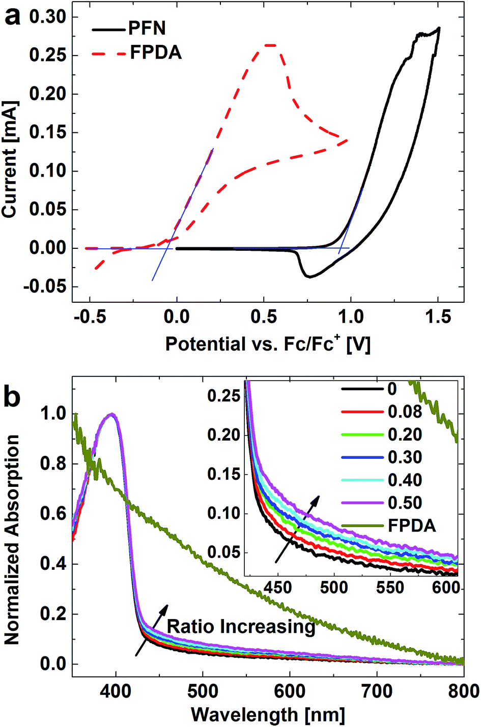 | ||
| Fig. 2 (a) Cyclic voltammetry of FPDA and PFN. (b) Normalized absorption spectra of FPDA and FPDA:PFN blend films. The zoom-in curves around 450 nm are shown in the inset, and the number represents the FPDA:PFN weight ratio. | ||
When used as the buffer layer at the bottom electrode, which is the “window material” transmitting light in a certain range of wavelength for adequate absorption of active layer, the HCBL should maintain the absorption of the host material (PFN) and not cause additional light consumption. According to Fig. 2b, the normalized FPDA absorption has a decreasing trend from 350 nm to 800 nm, and the absorption of HCBL with different FPDA content could be regarded as the superposition of the absorptions of PFN host material and FPDA modifier. Although the absolute absorption value of FPDA is much lower than that of PFN, the slightly gradual increase in absorption with FPDA content still could be observed at wavelength higher than 400 nm.
From above it can be seen that, in principle, the ionization and absorption characteristics of FPDA Lewis base could satisfy the requirements for the interface modification of inverted device structure, implying its suitability in improving the electrical contact. The feasibility of these two selection criteria for the interface modifier will be demonstrated in the following text.
3.2. Inhibition of interface exciton quenching
In order to investigate the modification effect of FPDA on the interface between active layer and cathode buffer layer, the 5 nm thickness HCBL with different FPDA content in PFN was first spin coated on the glass substrate, which was then covered by the spin-coated PBDT-TFQ film with 80 nm of thickness. The absorption spectra shown in Fig. S1† indicate no significant difference in the light absorptions, implying the negligible impact of occasional film geometric discrepancy.The steady-state PL spectra were collected through the same film-stacking configuration (the inset of Fig. 3a) and the excitation wavelength was set at 500 nm to avoid the fluorescence activity range of PFN (Fig. S2†). In addition, the FPDA modifier does not show observable fluorescent activity in the involved wavelength range. Therefore, the spectra shown in Fig. 3a are purely derived from the PL signal of PBDT-TFQ layer, which indicate that the PL intensity of PBDT-TFQ layer exhibits a positive correlation with FPDA content in HCBL. Since the only variable in the PL measurement is the FPDA content, it is speculated that the variation in the PL intensity is related to the interface states at the contact, the passivation of which could inhibit the exciton quenching.
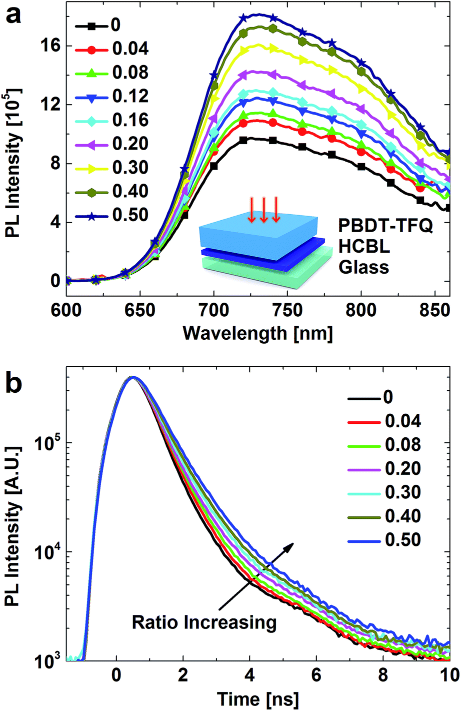 | ||
| Fig. 3 (a) PL spectra of PBDT-TFQ films deposited on FPDA:PFN blend films with weight ratio ranging from 0 to 0.50. The film stacking sequence is depicted in the inset. (b) Time resolved luminescence decay of the corresponding PBDT-TFQ films. | ||
The inhibition of exciton quenching resulted from FPDA interface modifier could be demonstrated by the time resolved luminescence. The decay curves in Fig. 3b show a stepwise tilt towards the longer time direction, indicating the extended PL lifetime with increased FPDA content in HCBL. In combination with the steady-state PL data (Fig. 3a), it is reasonable to deduce that the addition of FPDA interface modifier could passivate the interface quenching centres and thus decrease the possibility of the exciton non-radiative recombination. For photovoltaic devices, these effects could provide the excitons with longer lifetime for their diffusion toward the donor–acceptor heterojunction, which could facilitate the carrier generation process, result in higher short circuit current, and thus promote the device performance.
3.3. Enhancement of HCBL hole-blocking ability
Generally, the promotion of the photoelectric properties at the presence of the cathode buffer layer is achieved through its hole-blocking effect, which ensures the carrier collection at the respective electrodes and inhibits carrier recombination at cathode interface.5 In this study, the device with the stacking sequence of Ag/MoO3/PBDT-TFQ/HCBL/ITO (inset in Fig. 4a) was fabricated, and the hole-blocking capability between the pure donor and the HCBL could be deduced from the corresponding impedance characteristics.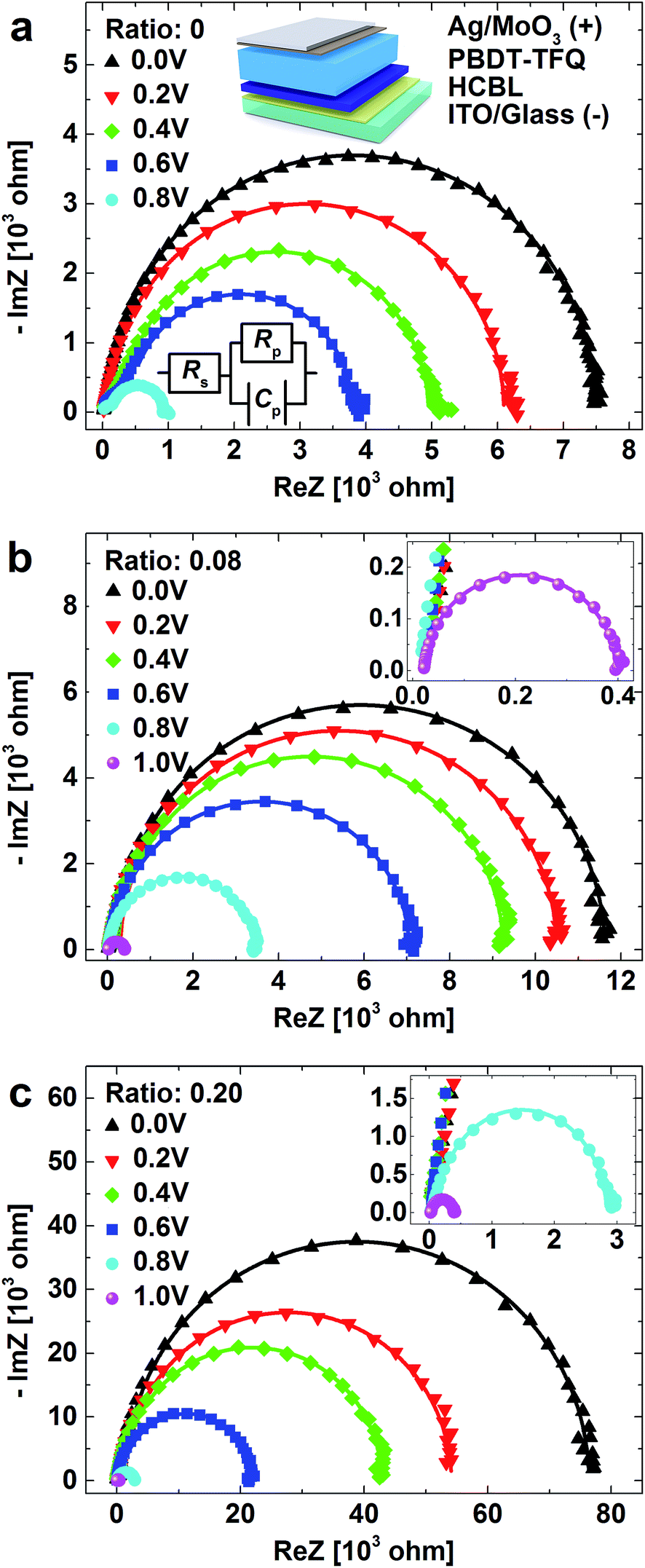 | ||
| Fig. 4 Nyquist plots under various applied bias for the devices with (a) 0, (b) 0.08, and (c) 0.2 of FPDA:PFN weight ratio in HCBL. The solid lines are the fit results. The insets in (a) are the schematic illustrations of the film stacking configuration and the equivalent circuit, respectively. The insets in (b) and (c) are the corresponding zoom-in curves at higher bias range. | ||
Fig. 4 is the Nyquist plots of the devices (structure illustrated in the inset of Fig. 4a) based on HCBL with 0, 0.08 and 0.20 of FPDA:PFN ratio. It can be seen that all the plots present “semicircular” shape, indicating homogeneous carrier transport pathway without discernible multiple interfacial boundaries. This characteristic ensures the feasibility of the proposed simplified equivalent circuit model, as shown in the inset of Fig. 4a, in which the capacitance Cp parallel connected with resistance Rp is in series with the resistance Rs.35 In the simplified model, Rs is mainly derived from the circuit parasitic ohmic resistances, including the wire resistance, the contact resistance between the probe and the electrodes, and the sheet resistance of electrodes. Cp is associated with the depletion region of the hole-blocking barrier, and Rp is mostly contributed from the leakage current across the barrier. The fitted parameters (Rs, Rp, Cp) based on the stacking configuration with different FPDA content are summarized in Table S1.† Since the tests were conducted under similar conditions, all the devices show the similar Rs (relative to Rp with ∼103 Ω), which could also be reflected from the plots at high frequencies (near the origin). The important finding is that as the bias rises, the Rp decreases while Cp increases, which is attributed to the bias-induced offset of the built-in electric field across the space charge region. Under the same bias, it could also be observed that the Cp and Rp take significant variations for the devices with different FPDA content in HCBL. For example, when the FPDA:PFN weight ratio rises from 0 and 0.08 to 0.20 under 0 V of bias, the Rp increases by an order of magnitude from 7.40 kΩ and 11.40 kΩ to 75.00 kΩ, which could be reflected from the plots at low frequencies (away from the origin) and implies the increased barrier resistance. Correspondingly, the Cp decreases from 7.27 nF and 6.23 nF to 5.37 nF, indicating gradually increased thickness of the depletion region. The above discussion demonstrates that the adjustment of the thickness of the depletion region and the barrier resistance could be effectively implemented by adding FPDA interface modifier with different amount, and thus the enhanced hole-blocking capability of the HCBL could be realized.
The effect of the FPDA modifier could be supported in terms of the capacitance–frequency (C–f) and capacitance–voltage (C–V) tests. As shown in Fig. S3,† the systematic decrease in capacitance with increasing FPDA:PFN weight ratio is observed and the capacitance of the devices responds promptly to the AC signal in the range of 102 to 105 Hz. It can also be deduced from Fig. S3† that the frequency of 1 × 10³ Hz is appropriate to differentiate the capacitances of the devices with different FPDA content. Therefore, the following response of capacitance to the AC signal was conducted with this frequency under direct current (DC) bias sweep.
Fig. 5 is the result of the C–V measurement, and the standard Mott–Schottky analysis is applied to the C–V curves for the extraction of space charge density (NA) and flat band voltage (Vb). The slope of the Mott–Schottky plots in the linear region of the curves could be fitted with linear dash lines, and thus the NA could be estimated by the equation:
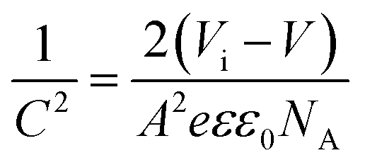 | (1) |
 | ||
| Fig. 5 Mott–Schottky plots of the devices structured as Ag/MoO3/PBDT-TFQ/HCBL/ITO with various FPDA:PFN ratio. | ||
The flat band voltage (Vb) derived from Fig. 5 is significantly shifted by the introduction of FPDA interface modifier (Table S2†), which demonstrates that the hole-blocking barrier height has been adjusted through the varied FPDA content. This is attributed to the regulated depletion region thickness in PBDT-TFQ, which indicates that interface states do influence the charge redistribution at the contact and results in the lower built-in field at electrostatic equilibrium. The Vb increases from 0.33 V of 0 FPDA:PFN weight ratio to 0.5 V of 0.20 that ratio, which is believed to be the main cause of the hole-blocking enhancement. In other words, the increased amount of FPDA could effectively suppress the influence of the interface states on the charge redistribution, and thus induces the thicker depletion region and consequent higher hole-blocking barrier.
The above discussion concerning the mechanism of the FPDA modification could be concisely illustrated in Fig. 6a and b, in which the interface states and energy level diagrams of PBDT-TFQ, PFN and HCBL layers are schematically shown (energy level diagrams for all components in the inverted photovoltaic devices are shown in Fig. S4†). Before the addition of FPDA, the deep located trap states at the PBDT-TFQ surface accommodate a certain number of electrons, which stimulate the additional electrical field and thus downward shift the band edges across the interface interval. Consequently, the Fermi level at the buffer layer side shifts to a relatively lower position, and a thinner depletion region in PBDT-TFQ is induced upon the electrostatic equilibrium establishment, indicating a lower hole-blocking barrier and serious interface carrier recombination. After introducing the interface modifier, part of the interface trap states is deactivated (Fig. 6b). As a result, the Fermi level is unpinned by reducing the interface charge accumulation and the attendant band edge shift, which induces a thicker depletion region in PBDT-TFQ for the electrostatic equilibrium, i.e. a higher hole-blocking barrier and the suppressed interface carrier recombination.
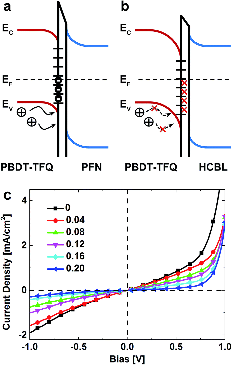 | ||
| Fig. 6 (a) and (b) are the schematic diagrams of energy level and surface states at the contact between PBDT-TFQ and PFN, and PBDT-TFQ and FPDA:PFN layers, respectively. EC, EF and EV are conduction band edge, Fermi level and valence band edge. (c) J–V plots of the devices with HCBL containing different FPDA:PFN ratio. | ||
The hole-blocking enhancement of FPDA interface modifier was further characterized through the J–V response of the same device configuration shown in Fig. 4a to simulate the loading variation in photovoltaic device tests. In Fig. 6c, it can be seen that the leakage current density, which is directly associated with the interface carrier recombination rate, varies nonlinearly with the increased bias, indicating the bias dependence of the hole-blocking ability. As the FPDA:PFN ration increases, the J–V curves gradually approach the lateral axis, indicating increased barrier resistance, which implies stronger suppression of interface charge recombination. However, it is noted that when the FPDA:PFN weight ratio is further increased to 0.50, the J–V response sharply subsides into the form of short circuit (shown in Fig. S5†). The above discussion demonstrates that the introduction of the FPDA in PFN layer could enhance the device PCE from the aspect of decreasing charge recombination at the cathode.
3.4. Passivation of HCBL electron-transport capability
From above it can be seen that the addition of FPDA could optimize the carrier generation process and enhance the HCBL hole-blocking ability. Based on these, one could easily deduce that the FPDA interface modifier should also influence the electron transport from the acceptor component of the active layer to the cathode. Fig. 7 gives the current response to the bias sweep of the devices with stacking configuration of Al/Ca/PBDT-TFQ:PC71BM/HCBL/ITO (inset of Fig. 7), which shows that as the FPDA content increases, the current density gradually decreases. This is especially obvious at higher bias and implies the passivation of the electron extraction capability. For photovoltaic devices, this passivation effect is unfavourable because it will exacerbate the interface carrier accumulation and induce local potential distortion. As a result, the carrier recombination is promoted and the built-in electrical field for the carrier extraction is partially consumed by the increased resistance, both of which give a worse fill factor (FF).
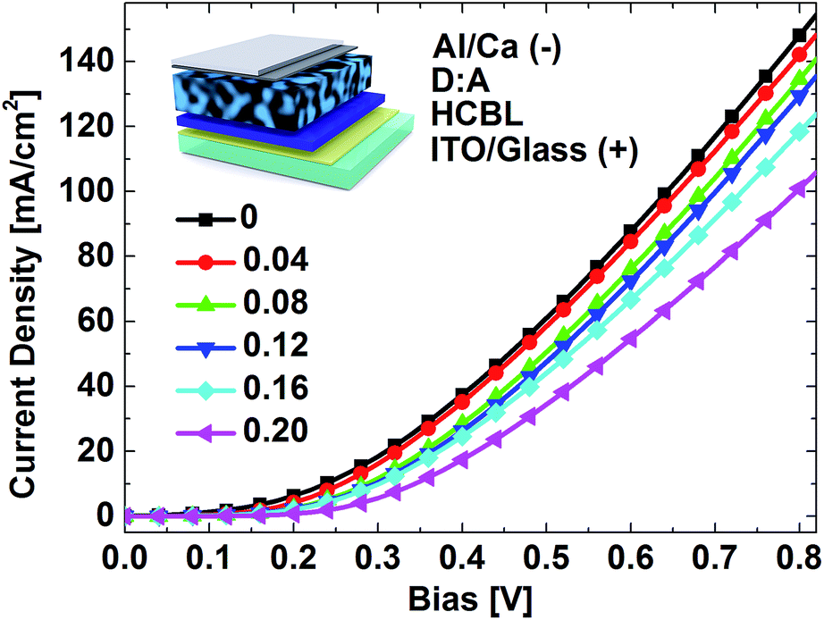 | ||
| Fig. 7 J–V characteristics of the electron only devices with and without FPDA. | ||
3.5. Joint contribution of HCBL modification effects to device performance
The above discussions elucidate that the HCBL containing FPDA interface modifier could regulate the carrier generation and extraction process, which exerts influence through inhibiting the interface exciton quenching, enhancing the hole-blocking capability, and passivating the electron transport behaviour. In order to estimate the overall effect of these factors, photovoltaic devices were fabricated based on the inverted configuration of Ag/MoO3/PBDT-TFQ:PC71BM/HCBL/ITO/glass which is schematically depicted in the inset of Fig. 8a (the corresponding cross-section SEM image is shown in Fig. S6†).
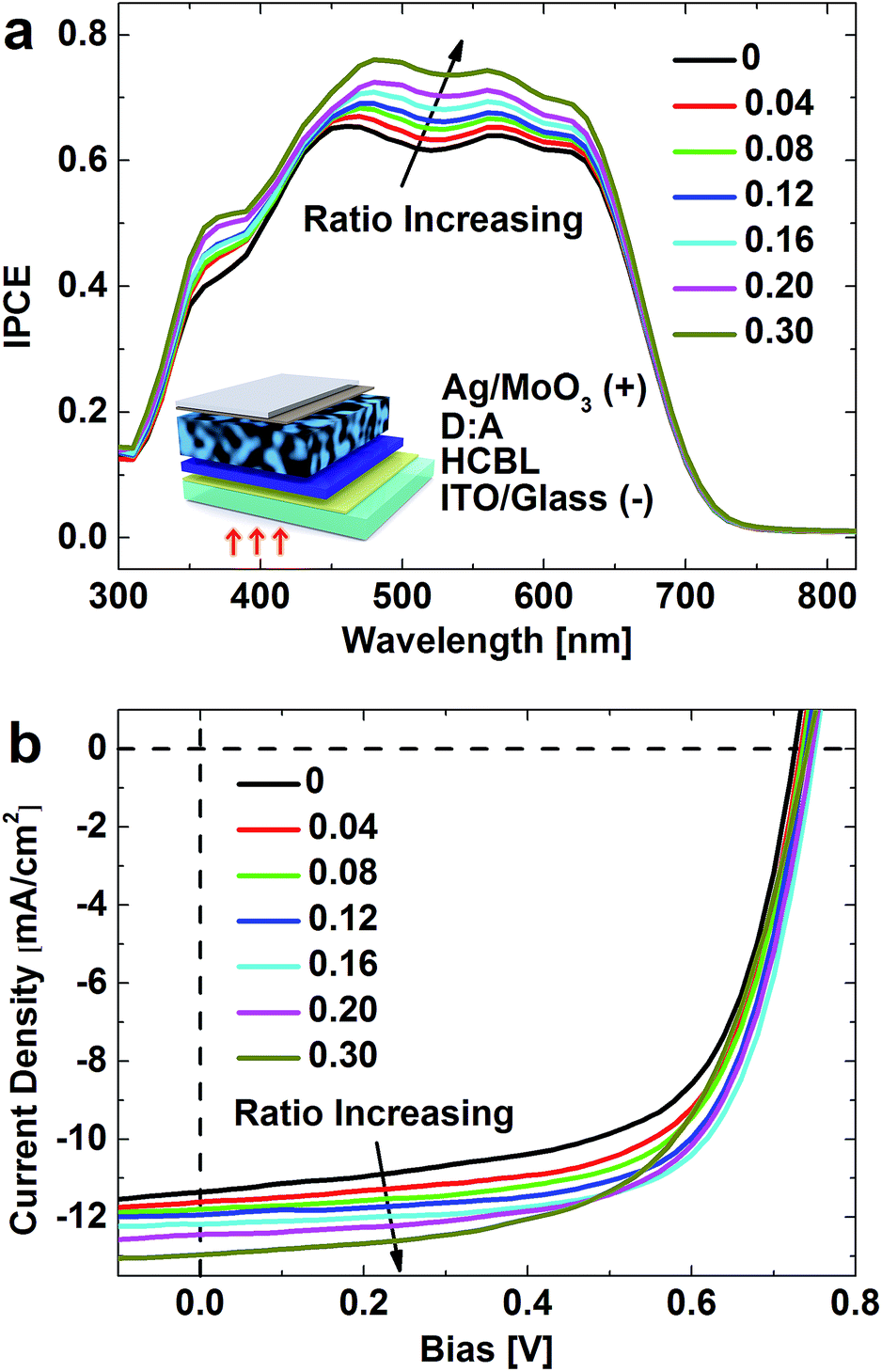 | ||
| Fig. 8 (a) IPCE of the devices with inverted structure depicted in the inset. (b) Device J–V response under illumination conditions in the bias range of carrier extraction. | ||
The extraction of photogenerated carriers under zero bias can be deduced from the incident photon-to-current efficiency (IPCE) spectra shown in Fig. 8a. The increased intensity of the spectra with FPDA:PFN ratio means the effectiveness of FPDA in boosting the photogenerated carriers. Previous discussions have demonstrated that this effect is partially derived from the modifier-induced inhibition of the interface exciton quenching, which facilitates the dissociation of a large amount of excitons, and partially from the enhanced hole-blocking capability through the suppression of the charge recombination at cathode, which thus achieves more efficient carrier extraction. Fig. 8a shows that the factor of passivating electron transport does not reverse the order of the spectra, indicating that a good trade-off is achieved in the FPDA:PFN ratio range of 0 to 0.30, at least under zero bias condition. It is noteworthy that the addition of the FPDA also brings the right shift of the peak in the range of 450 nm to 500 nm (from 460 nm to 490 nm), which involves the HCBL light shielding effect as discussed before and should also be taken into consideration for the interface modifier selection.
The joint contributions of inhibiting exciton quenching, enhancing hole-blocking and passivating electron transport were further characterized in terms of the maintenance of carrier extraction intensity against dynamic load under illumination of simulated AM1.5G condition. The obtained J–V characteristics are shown in Fig. 8b (the corresponding J–V curves under dark condition are shown in Fig. S7†), in which the negative and positive current density represent the carrier extraction and carrier injection dominant stages, respectively.
First of all, Fig. 8b shows a positive relationship between short circuit current (Jsc) and modifier content at zero-bias point, which is consistent with the IPCE results. As the bias increases (<0.4 V), the relationship remains. The addition of the interface modifier increases the shunt resistance (Rsh) and the open circuit voltage (Voc) of the devices (Table 1), suggesting a reduced leakage current caused by the enhanced hole-blocking ability, which is effective in reducing the carrier recombination and thus improving the rectification of the J–V response. It should be noted that the electron transport passivation induced by the FPDA do exist and increases with PFDA:PFN ratio, which could be reflected from the curves in the carrier injection region shown in Fig. S8† and confirmed by the device series resistance (Rsr) listed in Table 1. The J–V behaviour of the devices is actually the result of the joint contributions of hole-blocking enhancement and the electron transport passivation. As the FPDA content increases to 0.20, it is found from Fig. 8b that the onset of the drastic variation of the J–V curve around 0.6 V shifts to lower bias, which becomes obvious when the FPDA content reaches 0.30. Correspondingly, the device FF and PCE decrease sequentially after this composition point. In other words, when the FPDA content is higher than 0.16, the negative impact of the electron transport passivation becomes the dominant factor that determines the device performance.
:PFN weight ratioa
| Ratio | Voc [V] | Jsc [mA cm−2] | FF [%] | PCE [%] | Rsr [Ω cm2] | Rsh [Ω cm2] |
|---|---|---|---|---|---|---|
| a Statistical analysis and the average parameters for 8 devices are presented in Fig. S9. | ||||||
| 0 | 0.726 | 11.35 | 63.33 | 5.22 | 3.40 | 574.2 |
| 0.04 | 0.734 | 11.61 | 65.40 | 5.57 | 3.73 | 736.9 |
| 0.08 | 0.736 | 11.79 | 66.02 | 5.73 | 3.92 | 886.7 |
| 0.12 | 0.740 | 11.94 | 67.93 | 6.00 | 3.97 | 1046.0 |
| 0.16 | 0.750 | 12.18 | 68.34 | 6.24 | 4.04 | 1904.5 |
| 0.20 | 0.746 | 12.44 | 65.94 | 6.12 | 4.64 | 1318.6 |
| 0.30 | 0.742 | 12.97 | 60.82 | 5.85 | 6.90 | 928.8 |
It is known from above discussions that three factors, i.e. the inhibition of interface exciton quenching, hole-blocking enhancement and electron-transport passivation, are induced by introducing FPDA interface modifier. Among them, the inhibition of interface exciton quenching facilitates the carrier generation process, the enhanced hole-blocking ability is effective in reducing the interface carrier recombination, and these two factors are positive for device performance. The passivation of electron-transport capability is negative and it could exacerbate the interface charge accumulation. The final device performance depends on the trade-off between these three factors. As listed in Table 1, when the FPDA content is lower than 0.16, the interface exciton quenching and hole-blocking enhancement are the two dominant and favourable factors, and thus the device PCE increases from 5.22% to 6.00%. The best PCE of 6.24% is realized for 0.16 FPDA:PFN ratio, which is increased by almost 20% in comparison to the original PCE (5.22%) and indicates that the optimal trade-off between these three factors is reached. However, if the FPDA content further increases, the negative effect of the electron transport passivation emerges to be the dominant factor and thus the device PCE deteriorates. The variation in the device efficiency with the FPDA content could be directly observed from the power density–voltage (P–V) curves, as shown in Fig. S10,† in which the optimum power-output point shows the trend of first increase and then decrease with the highest value at 0.16 of FPDA:PFN weight ratio.
In this study, FPDA, which is one of the Lewis bases and possesses lower ionization energy, is selected as the interface modifier to blend with the PFN host material, and thus resultant HCBL is demonstrated to could effectively mitigate the disturbance of the interface states. Although more studies need to be conducted, in principle, the interface modification strategy based on HCBL should also be applicable for other small molecule compounds with similar structures and properties and for the cases where the interface states create significant disturbance for a desired energy band configuration at the contacts. In addition, the wide loading window of the interface modifier also provides the photoelectric devices with flexibly regulated interface electrical properties.
4. Conclusions
In conclusion, interface modification strategy based on the HCBL composed of FPDA as the interface modifier and PFN as the host material is proposed and demonstrated. By introducing FPDA, the carrier generation is systematic promoted through the inhibition of interface exciton quenching. Moreover, the hole-blocking ability of HCBL is gradually enhanced with increased FPDA:PFN ratio, which is proved to be caused by the unpinning of Fermi level. The introduction of FPDA also passivates the electron transport capability of the HCBL, suggesting the necessity of elegant adjustment of the FPDA:PFN ratio. The joint contribution of these three factors shows significant effect on the carrier generation and extraction processes. As a result, the PCE reaches 6.24% for the device with HCBL of 0.16 FPDA:PFN ratio, which is much higher than 5.22% of the pristine one. In addition, the improved device performance is realized for the device with HCBL containing FPDA:PFN weight ratio lower than 0.16, demonstrating the wide loading range of the interface modifier. This interface modification strategy is effective, controllable, and easy to solution processing, which is expected to could be used in the effort to promote the performances of both the buffer layers and the photovoltaic devices.
Acknowledgements
This work was supported by the National Natural Science Foundation of China (Grant No. 21574132, 21504090).References
- L. Lu, T. Zheng, Q. Wu, A. M. Schneider, D. Zhao and L. Yu, Chem. Rev., 2015, 150807151721002 Search PubMed.
- F. C. Krebs, N. Espinosa, M. Hösel, R. R. Søndergaard and M. Jørgensen, Adv. Mater., 2014, 26, 29–39 CrossRef CAS PubMed.
- L. Dou, J. You, Z. Hong, Z. Xu, G. Li, R. A. Street and Y. Yang, Adv. Mater., 2013, 25, 6642–6671 CrossRef CAS PubMed.
- C. Duan, W. Cai, B. B. Y. Hsu, C. Zhong, K. Zhang, C. Liu, Z. Hu, F. Huang, G. C. Bazan, A. J. Heeger and Y. Cao, Energy Environ. Sci., 2013, 6, 3022 CAS.
- W. Tress, K. Leo and M. Riede, Phys. Rev. B: Condens. Matter Mater. Phys., 2012, 85, 155201 CrossRef.
- H.-L. Yip and A. K.-Y. Jen, Energy Environ. Sci., 2012, 5, 5994 CAS.
- W. E. Ford, D. Gao, N. Knorr, R. Wirtz, F. Scholz, Z. Karipidou, K. Ogasawara, S. Rosselli, V. Rodin, G. Nelles and F. von Wrochem, ACS Nano, 2014, 8, 9173–9180 CrossRef CAS PubMed.
- Y. J. Lee, J. Wang, S. R. Cheng and J. W. P. Hsu, ACS Appl. Mater. Interfaces, 2013, 5, 9128–9133 CAS.
- A. Guerrero, L. F. Marchesi, P. P. Boix, S. Ruiz-Raga, T. Ripolles-Sanchis, G. Garcia-Belmonte and J. Bisquert, ACS Nano, 2012, 6, 3453–3460 CrossRef CAS PubMed.
- J.-H. Lee and J.-J. Kim, Phys. Status Solidi, 2012, 209, 1399–1413 CrossRef CAS.
- F. Bussolotti, J. Yang, A. Hinderhofer, Y. Huang, W. Chen, S. Kera, A. T. S. Wee and N. Ueno, Phys. Rev. B: Condens. Matter Mater. Phys., 2014, 89, 115319 CrossRef.
- J. Song, K. Goh, N. Chandrasekhar and C. Troadec, Phys. Rev. B: Condens. Matter Mater. Phys., 2009, 79, 165313 CrossRef.
- Z. Jia, V. W. Lee, I. Kymissis, L. Floreano, A. Verdini, A. Cossaro and A. Morgante, Phys. Rev. B: Condens. Matter Mater. Phys., 2010, 82, 125457 CrossRef.
- J. A. Carr and S. Chaudhary, Energy Environ. Sci., 2013, 6, 3414 CAS.
- M. Hartel, S. Chen, B. Swerdlow, H.-Y. Hsu, J. Manders, K. Schanze and F. So, ACS Appl. Mater. Interfaces, 2013, 5, 7215–7218 CAS.
- M. T. Greiner and Z.-H. Lu, NPG Asia Mater., 2013, 5, e55 CrossRef CAS.
- O. J. Sandberg, M. Nyman and R. Österbacka, Phys. Rev. Appl., 2014, 1, 024003 CrossRef.
- M. Hirade and C. Adachi, Appl. Phys. Lett., 2011, 99, 153302 CrossRef.
- S. Yogev, R. Matsubara, M. Nakamura, U. Zschieschang, H. Klauk and Y. Rosenwaks, Phys. Rev. Lett., 2013, 110, 036803 CrossRef CAS PubMed.
- P. Amsalem, J. Niederhausen, A. Wilke, G. Heimel, R. Schlesinger, S. Winkler, A. Vollmer, J. P. Rabe and N. Koch, Phys. Rev. B: Condens. Matter Mater. Phys., 2013, 87, 035440 CrossRef.
- M. Oehzelt, N. Koch and G. Heimel, Nat. Commun., 2014, 5, 1–8 Search PubMed.
- D. Belaineh, J.-K. Tan, R.-Q. Png, P.-F. Dee, Y.-M. Lee, B.-N. N. Thi, N.-S. Ridzuan and P. K. H. Ho, Adv. Funct. Mater., 2015, 25, 5504–5511 CrossRef CAS.
- B. Ray, A. G. Baradwaj, M. R. Khan, B. W. Boudouris and M. A. Alam, Proc. Natl. Acad. Sci. U. S. A., 2015, 112, 11193–11198 CrossRef CAS PubMed.
- M. L. Tietze, P. Pahner, K. Schmidt, K. Leo and B. Lüssem, Adv. Funct. Mater., 2015, 25, 2701–2707 CrossRef CAS.
- Y.-M. Chang, R. Zhu, E. Richard, C.-C. Chen, G. Li and Y. Yang, Adv. Funct. Mater., 2012, 22, 3284–3289 CrossRef CAS.
- Y. Zhou, C. Fuentes-Hernandez, J. Shim, J. Meyer, A. J. Giordano, H. Li, P. Winget, T. Papadopoulos, H. Cheun, J. Kim, M. Fenoll, A. Dindar, W. Haske, E. Najafabadi, T. M. Khan, H. Sojoudi, S. Barlow, S. Graham, J.-L. Bredas, S. R. Marder, A. Kahn and B. Kippelen, Science, 2012, 336, 327–332 CrossRef CAS PubMed.
- L. Lindell, M. P. de Jong, W. Osikowicz, R. Lazzaroni, M. Berggren, W. R. Salaneck and X. Crispin, J. Chem. Phys., 2005, 122, 1–12 CrossRef PubMed.
- W. Osikowicz, X. Crispin, C. Tengstedt, L. Lindell, T. Kugler and W. R. Salaneck, Appl. Phys. Lett., 2004, 85, 1616–1618 CrossRef CAS.
- Z. A. Page, Y. Liu, V. V. Duzhko, P. Thomas, T. Emrick, T. P. Russell and T. Emrick, Science, 2014, 346, 441 CrossRef CAS PubMed.
- B. Qi, Z.-G. Zhang and J. Wang, Sci. Rep., 2015, 5, 7803 CrossRef CAS PubMed.
- A. Savva, F. Petraki, P. Elefteriou, L. Sygellou, M. Voigt, M. Giannouli, S. Kennou, J. Nelson, D. D. C. Bradley, C. J. Brabec and S. A. Choulis, Adv. Energy Mater., 2013, 3, 391–398 CrossRef CAS.
- H. C. Chen, Y. H. Chen, C. C. Liu, Y. C. Chien, S. W. Chou and P. T. Chou, Chem. Mater., 2012, 24, 4766–4772 CrossRef CAS.
- J.-B. Baek and F. W. Harris, Macromolecules, 2005, 38, 297–306 CrossRef CAS.
- W. Zhao, L. Ye, S. Zhang, B. Fan, M. Sun and J. Hou, Sci. Rep., 2014, 4, 6570 CrossRef CAS PubMed.
- T. J. Savenije, E. Moons, G. K. Boschloo, A. Goossens and T. J. Schaafsma, Phys. Rev. B: Condens. Matter Mater. Phys., 1997, 55, 9685–9692 CrossRef CAS.
Footnote |
| † Electronic supplementary information (ESI) available: UV-Vis spectra of PBDT-TFQ/FPDA:PFN films; PL spectra of PFN film; C–f plots of the film configuration for impedance measurement; film J–V characteristics with excessive FPDA content; device J–V curves under dark condition; device J–V curves and P–V curves under illumination; statistical analysis of device parameters; fitted data of the Nyquist plots and the C–V plots. See DOI: 10.1039/c5ra23163a |
| This journal is © The Royal Society of Chemistry 2016 |