CdS–phenanthroline derivative hybrid cathode interlayers for high performance inverted organic solar cells†
Xiaohui
Liu‡
ab,
Yulei
Wu‡
a,
Xiaodong
Li
ab,
Wenjun
Zhang
a,
Lixiao
Zhao
a,
Hai-Qiao
Wang
*a and
Junfeng
Fang
*a
aNingbo Institute of Materials Technology and Engineering, Chinese Academy of Sciences, Ningbo 315201, China. E-mail: hqwang@nimte.ac.cn; fangjf@nimte.ac.cn
bUniversity of Chinese Academy of Sciences, Beijing 100049, China
First published on 9th November 2015
Abstract
Phenanthroline based organic semiconductors (BCP, Bphen, Mphen, and Phen) are used to hybrid with CdS as cathode interlayers in inverted organic solar cells (OSCs). We observed that selecting the polar solvent and hydrophobic interlayers with a diphenyl group could improve the performance of the organic photovoltaic devices. The modification to CdS can effectively improve its electron mobility, film morphology, interfacial contact, and energy level alignment, which finally leads to a significant enhancement of device performance. Through incorporating the CdS–P hybrids (CdS–BCP, CdS–Bphen, CdS–Mphen, and CdS–Phen) as cathode buffer layers, the device PCE (PTB7![[thin space (1/6-em)]](https://www.rsc.org/images/entities/char_2009.gif) :
:![[thin space (1/6-em)]](https://www.rsc.org/images/entities/char_2009.gif) PC71BM as the active layer) is greatly improved from 3.09% to 8.36, 7.84, 6.69, and 6.57%, respectively, compared with devices fabricated on the pristine CdS interlayer. These results indicate that the common inorganic semiconductor like CdS can be modified using some organic semiconductors to produce general applicable electron transport layers applied in OSCs. Our work puts forward new insights for the development of new interface modification materials and fabrication of high efficiency devices.
PC71BM as the active layer) is greatly improved from 3.09% to 8.36, 7.84, 6.69, and 6.57%, respectively, compared with devices fabricated on the pristine CdS interlayer. These results indicate that the common inorganic semiconductor like CdS can be modified using some organic semiconductors to produce general applicable electron transport layers applied in OSCs. Our work puts forward new insights for the development of new interface modification materials and fabrication of high efficiency devices.
Introduction
Solution-processed bulk heterojunction organic solar cells (OSCs) have attracted considerable attention due to their advantages of low cost, lightweight, flexibility and potential for large-scale manufacturing.1–3 In the past decades, enormous progress has been achieved in improving the performance of OSCs and a promising power conversion efficiency (PCE) of ∼10% has been reported by several research groups based on different active blends.4–8 Besides active materials, the interfacial layers between the active layer and electrodes play an important role as well in delivering a high power conversion efficiency for organic solar cells.9,10 The contact of the organic/electrode interface can significantly affect the parameters like open-circuit voltage (Voc), short-circuit current (Jsc) and fill factor (FF) due to its abilities to tune the energy level alignment,11,12 improve charge transport at the interface,13 promote the adhesion between the electrode and active layer and enhance light-trapping by the optical spacer effect.14,15 Until now, different p-/n-type interfacial materials including conjugate polyelectrolytes,10,16 crosslinkable materials,17 small molecules,18 inorganic materials like metal oxides,19–21 and even ultra-thin/monolayer organic molecule modified metal oxides22–24 have been utilized in organic solar cells, and most of them can deliver fair device performance. However, challenges are still there and more effort is needed in this field to promote the device performance.Recently, as a further development of the thin organic molecule modifying interlayer strategy, a new type of organic–inorganic bulk-hybrid interlayer comes into the focus of this research field and some significant advances have been made in the corresponding solar cells. These interlayers are composed of hybrid materials synthesized with corresponding organic and inorganic components and hence they combine the advantages of both part like good conductivity and compatibility. In 2013, by using the Zn–C60 hybrid electron transport layer, Chen et al. achieved much improved performance for the P3HT![[thin space (1/6-em)]](https://www.rsc.org/images/entities/char_2009.gif) :
:![[thin space (1/6-em)]](https://www.rsc.org/images/entities/char_2009.gif) IC60BA (5.29–6.6%), PTB7
IC60BA (5.29–6.6%), PTB7![[thin space (1/6-em)]](https://www.rsc.org/images/entities/char_2009.gif) :
:![[thin space (1/6-em)]](https://www.rsc.org/images/entities/char_2009.gif) PC71BM (6.65–8.21%) and PTB7-Th
PC71BM (6.65–8.21%) and PTB7-Th![[thin space (1/6-em)]](https://www.rsc.org/images/entities/char_2009.gif) :
:![[thin space (1/6-em)]](https://www.rsc.org/images/entities/char_2009.gif) PC71BM (7.64–9.35%) blend-based devices, compared to the pristine ZnO interfacial layer device.25 In 2014, they developed a new dual-doped ZnO interfacial material InZnO-BisC60, with which a new record PCE of 10.31% was achieved for single junction polymer solar cells based on the PTB7-Th
PC71BM (7.64–9.35%) blend-based devices, compared to the pristine ZnO interfacial layer device.25 In 2014, they developed a new dual-doped ZnO interfacial material InZnO-BisC60, with which a new record PCE of 10.31% was achieved for single junction polymer solar cells based on the PTB7-Th![[thin space (1/6-em)]](https://www.rsc.org/images/entities/char_2009.gif) :
:![[thin space (1/6-em)]](https://www.rsc.org/images/entities/char_2009.gif) PC71BM blend with the same device architecture.26 In the same year, a similar functionality was demonstrated for a poly(9,9-bis-(6′-diethoxylphosphorylhexyl) fluorene) (PFEP) conjugated ZnO hybrid interlayer (ZnO–PFEP) in P(IID-DTC)
PC71BM blend with the same device architecture.26 In the same year, a similar functionality was demonstrated for a poly(9,9-bis-(6′-diethoxylphosphorylhexyl) fluorene) (PFEP) conjugated ZnO hybrid interlayer (ZnO–PFEP) in P(IID-DTC)![[thin space (1/6-em)]](https://www.rsc.org/images/entities/char_2009.gif) :
:![[thin space (1/6-em)]](https://www.rsc.org/images/entities/char_2009.gif) PC70BM based polymer solar cells by Xie et al.27 Enhanced PCE up to 7.56% for the ZnO–PFEP buffered device was achieved compared to the PCE of 5.24% with the pure ZnO interlayer device. Besides that, the conductive ZnO–PFEP allows a much larger thickness as the interfacial layer, benefiting the device reproducibility in large-scale printable techniques. In our previous work, we also reported an organic–inorganic hybrid interfacial material CdS/2,9-dimethyl-4,7-diphenyl-1,10-phenanthroline (CdS–BCP).28 The hybrid chemical structure was demonstrated by the chemical bond between the two units verified by the X-ray photoelectron spectroscopy (XPS) analysis. As the electron transporting layer, it delivered a high PCE of 7.47% for the inverted PTB7
PC70BM based polymer solar cells by Xie et al.27 Enhanced PCE up to 7.56% for the ZnO–PFEP buffered device was achieved compared to the PCE of 5.24% with the pure ZnO interlayer device. Besides that, the conductive ZnO–PFEP allows a much larger thickness as the interfacial layer, benefiting the device reproducibility in large-scale printable techniques. In our previous work, we also reported an organic–inorganic hybrid interfacial material CdS/2,9-dimethyl-4,7-diphenyl-1,10-phenanthroline (CdS–BCP).28 The hybrid chemical structure was demonstrated by the chemical bond between the two units verified by the X-ray photoelectron spectroscopy (XPS) analysis. As the electron transporting layer, it delivered a high PCE of 7.47% for the inverted PTB7![[thin space (1/6-em)]](https://www.rsc.org/images/entities/char_2009.gif) :
:![[thin space (1/6-em)]](https://www.rsc.org/images/entities/char_2009.gif) PC71BM device compared to the PCE of 4.77% and 6.57% of the reference devices with CdS and BCP as the interlayer, respectively, and improved the device stability very much compared to the conventional PEDOT:PSS buffered device. Furthermore, the hybrid-interlayer strategy has also been utilized in other types of photovoltaic devices like perovskite solar cells and has shown great potential.29,30 Although hybrid interfacial layers present promising potential in solar cells and remarkable improvements have been achieved, still there are very limited studies and most of them have focused on ZnO-based hybrid systems especially on organic solar cells. We believe it is worth putting more effort in this hybrid interlayer technique to understand the underlying fundamental mechanism, explore and develop more efficient hybrid interlayers and even its application in other types of photovoltaic devices.
PC71BM device compared to the PCE of 4.77% and 6.57% of the reference devices with CdS and BCP as the interlayer, respectively, and improved the device stability very much compared to the conventional PEDOT:PSS buffered device. Furthermore, the hybrid-interlayer strategy has also been utilized in other types of photovoltaic devices like perovskite solar cells and has shown great potential.29,30 Although hybrid interfacial layers present promising potential in solar cells and remarkable improvements have been achieved, still there are very limited studies and most of them have focused on ZnO-based hybrid systems especially on organic solar cells. We believe it is worth putting more effort in this hybrid interlayer technique to understand the underlying fundamental mechanism, explore and develop more efficient hybrid interlayers and even its application in other types of photovoltaic devices.
Considering that BCP and 4,7-diphenyl-1,10-phenanthroline (Bphen) have been widely utilized in luminescent and photovoltaic devices as the hole blocking/electron transport layer, excellent electrical properties of the CdS inorganic semiconductor, and promising performance of the CdS–BCP hybrid interlayer solar cells achieved in our previous work, in this study, we systematically investigate the use of CdS-organic hybrid interlayer systems in PTB7![[thin space (1/6-em)]](https://www.rsc.org/images/entities/char_2009.gif) :
:![[thin space (1/6-em)]](https://www.rsc.org/images/entities/char_2009.gif) PC71BM solar cells. Phenanthroline and its derivatives Bphen, 2,9-dimethyl-1,10-phenanthroline (Mphen) and 1,10-phenanthroline (Phen) are utilized as substitutes for BCP to modify CdS, forming hybrid interfacial materials CdS–Bphen, CdS–Mphen, and CdS–Phen. All of them outperform the pristine CdS when incorporated into PTB7
PC71BM solar cells. Phenanthroline and its derivatives Bphen, 2,9-dimethyl-1,10-phenanthroline (Mphen) and 1,10-phenanthroline (Phen) are utilized as substitutes for BCP to modify CdS, forming hybrid interfacial materials CdS–Bphen, CdS–Mphen, and CdS–Phen. All of them outperform the pristine CdS when incorporated into PTB7![[thin space (1/6-em)]](https://www.rsc.org/images/entities/char_2009.gif) :
:![[thin space (1/6-em)]](https://www.rsc.org/images/entities/char_2009.gif) PC71BM blend solar cells. And the CdS–BCP hybrid interlayer delivers the best power conversion efficiency of 8.36%.
PC71BM blend solar cells. And the CdS–BCP hybrid interlayer delivers the best power conversion efficiency of 8.36%.
Experimental
Materials and methods
CdCl2, KS2COEt and pyridine were bought from Aladdin Reagent. BCP, Bphen, Mphen and Phen were obtained from Alfa Aesar. PTB7 and PC71BM were purchased from 1-Material and ADS, respectively. All the available materials were used as received without any further purification.The detailed preparation of cadmium xanthate (Cd(S2COEt)2) is described in the literature.28,31 BCP was added into a stirring suspension solution of Cd(S2COEt)2 in chloroform. The suspension immediately changed to yellow solution after being stirred for 2 hours and then filtered. The obtained clear filtrate was left to crystallize by slow evaporation of the solvent. And then the crude product of Cd(S2COEt)2·(BCP) was purified by recrystallization from chloroform twice. Cd(S2COEt)2·(Bphen), Cd(S2COEt)2·(Mphen), Cd(S2COEt)2·(Phen), and Cd(S2COEt)2·(C5H5N)2 crystals were prepared with the same route.
Device fabrication
Pre-patterned indium tin oxide (ITO)-coated glass with a sheet resistance of 10 Ω per square was used as the substrate. It was cleaned by sequential sonication in detergent, deionized water, acetone, and isopropanol for 15 min at each step. After ultraviolet-ozone treatment for 30 min, the CdS–phenanthroline derivative (CdS–P) precursors were spin-coated onto ITO substrates at 5000 rpm and then annealed at 175 °C for 30 min. The thicknesses of the CdS–P layers and CdS layer after annealing were about 20 nm. Then the photoactive layer was deposited on top of the hybrid interlayers by spin-coating from the blend solution of PTB7![[thin space (1/6-em)]](https://www.rsc.org/images/entities/char_2009.gif) :
:![[thin space (1/6-em)]](https://www.rsc.org/images/entities/char_2009.gif) PC71BM dissolved in chlorobenzene/1,8-diiodoctane (97
PC71BM dissolved in chlorobenzene/1,8-diiodoctane (97![[thin space (1/6-em)]](https://www.rsc.org/images/entities/char_2009.gif) :
:![[thin space (1/6-em)]](https://www.rsc.org/images/entities/char_2009.gif) 3 vol%) under 2000 rpm for 120 seconds, and the ratio of PTB7
3 vol%) under 2000 rpm for 120 seconds, and the ratio of PTB7![[thin space (1/6-em)]](https://www.rsc.org/images/entities/char_2009.gif) :
:![[thin space (1/6-em)]](https://www.rsc.org/images/entities/char_2009.gif) PC71BM was 1
PC71BM was 1![[thin space (1/6-em)]](https://www.rsc.org/images/entities/char_2009.gif) :
:![[thin space (1/6-em)]](https://www.rsc.org/images/entities/char_2009.gif) 1.5 by weight (25 mg mL−1). The device fabrication was finished by thermally evaporating a 10 nm MoO3 layer and a 100 nm Al anode at a vacuum level of 2 × 10⁻⁶ Torr. All the devices were fabricated under the same conditions and with an effective device area of 0.06 cm2. The electron-only devices were made as the structure of ITO/CdS or CdS–P/PTB7
1.5 by weight (25 mg mL−1). The device fabrication was finished by thermally evaporating a 10 nm MoO3 layer and a 100 nm Al anode at a vacuum level of 2 × 10⁻⁶ Torr. All the devices were fabricated under the same conditions and with an effective device area of 0.06 cm2. The electron-only devices were made as the structure of ITO/CdS or CdS–P/PTB7![[thin space (1/6-em)]](https://www.rsc.org/images/entities/char_2009.gif) :
:![[thin space (1/6-em)]](https://www.rsc.org/images/entities/char_2009.gif) PC71BM/LiF/Al.
PC71BM/LiF/Al.
Characterization
J–V characteristics of photovoltaic cells were measured using a Keithley 2440 sourcemeter under the irradiation of a simulated AM1.5G solar spectrum with an Oriel Sol3A solar simulator. External quantum efficiency (EQE) was measured by using a Newport quantum efficiency measurement system (ORIEL IQE 200 TM) with a lock-in amplifier and a 150 W xenon lamp under ambient atmosphere at room temperature. The light intensity at each wavelength was calibrated with a standard single-crystal Si/Ge photovoltaic cell.Ultra-violet photoelectron spectroscopy (UPS) and XPS were performed using a Kratos AXIS ULTRA DLD XPS/UPS system. UPS was carried out using He I radiation at 21.21 eV from a discharge lamp operated at 20 mA, a pass energy of 5 eV, and a channel width of 25 meV. A −7.35 V bias was applied to the samples in order to separate the sample and analyze low-kinetic-energy cutoffs. For XPS, survey scans to identify the overall surface composition were carried out using a monochromatic Al Kα X-ray source (1486.6 eV). High-resolution scans to identify bonding states were performed at 20 eV pass energy and 50 meV channel width. All the spectra were adjusted according to the standard value of C 1s peak at 284.8 eV. The surface morphology of the hybrid buffer layers was investigated using a field-emission scanning electron microscope (FE-SEM) (Hitachi S-4800). Droplet images were recorded on a contact-angle system (model OCA20) and the film thickness was measured under a Veeco Dektak 150.
Results and discussion
In our previous work, based on the solution-processable precursor Cd(S2COEt)2·(BCP) (dissolved in acetone, 10 mg mL−1), the hybrid CdS–BCP cathode interlayer was prepared by thermal annealing. The hybrid molecule structure was confirmed by the chemical bond of Cd–N verified by the XPS analysis (Fig. S1†). And a power conversion efficiency of 7.47% has been achieved in inverted OSCs.28To further investigate this hybrid interlayer system and optimize the device performance, in this study, we firstly investigated the influence of the solvent on the hybrid interlayer. Various polar solvents like chloroform (CF), acetone (AT), tetrahydrofuran (THF), and N,N-dimethylformamide (DMF) with concentration gradients of 10 mg mL−1, 20 mg mL−1, and 30 mg mL−1 were applied to fabricate the hybrid interlayer CdS–BCP. Fig. S2† presents the current–voltage (J–V) characteristics of the obtained OSCs measured under AM 1.5G irradiation. The detailed parameters including short circuit current density (Jsc), open circuit voltage (Voc), fill factor (FF) and PCE are summarized in Table S1.† When processed using acetone with a concentration of 10 mg mL−1, the CdS–BCP hybrid interlayer delivered a PCE of 7.46%, with a Voc of 0.709 V, a Jsc of 16.81 mA cm−2 and a FF of 62.58%, which are consistent with our previously reported results.28 Obviously, processed with higher polar solvents (DMF, THF, AT), the hybrid interlayers deliver comparatively superior performances than that spin-cast from non-polar solvent CF. In more detail, the polar solvent DMF processed hybrid interlayer elevated the device performance to 7.76%, compared with AT (7.46%) with the same concentration of 10 mg mL−1, probably due to the higher boiling point and slower evaporation speed of DMF than AT, leading to a better film morphology, and hence better device performance (Fig. S3†).
Hence we chose the optimal solvent DMF to process all the different CdS–phenanthroline/derivative hybrid interlayers with a fixed concentration of 10 mg mL−1. Here, besides BCP, the organic parts such as Bphen, Mphen and Phen are selected to coordinate with Cd(S2COEt)2 to prepare cadmium chelate compound precursors Cd(S2COEt)2·(P) (P: BCP, Bphen, Mphen and Phen). The inverted OSCs configuration studied in this work and the molecular structure of BCP, Bphen, Mphen and Phen are shown in Fig. 1. The crystals of Cd(S2COEt)2·(P) are formed by slow evaporation of CF and purified by recrystallization twice. And the acquired precursors Cd(S2COEt)2·(P) were dissolved in DMF with a concentration of 10 mg mL−1 and spin-cast at 5000 rpm onto the ITO surface and annealed at 175 °C for 30 minutes to form the CdS–P hybrid electron transport interlayer, as depicted in Fig. 1. The characteristic J–V curves of the optimized OSCs with the device structure of ITO/CdS–P/PTB7![[thin space (1/6-em)]](https://www.rsc.org/images/entities/char_2009.gif) :
:![[thin space (1/6-em)]](https://www.rsc.org/images/entities/char_2009.gif) PC71BM/MoO3/Al are presented in Fig. 2a and Table 1. For comparison, a control device with the interlayer of pristine CdS decomposed from its precursor Cd(S2COEt)2·(pyridine)2 was fabricated and tested as well. The devices based on the hybrid materials of CdS–BCP exhibit the best performance, with PCE increased from 3.09% to 8.36%, and the main parameters of Voc, Jsc and FF improved from 0.404 V, 15.27 mA cm−2, and 50.13% to 0.722 V, 17.42 mA cm−2, and 66.44%, respectively, compared to that with CdS. The CdS–Bphen devices present remarkably increased performance as well relative to that with CdS, with PCE increased from 3.09% to 7.84%. Besides that, Voc, Jsc, and FF are increased by 76%, 12.8%, and 27.7%, respectively. While for the devices fabricated with CdS–Mphen and CdS–Phen, relatively lower performances are obtained. As presented in Table 1, relatively low series resistances (Rs) and high shunt resistances (Rsh) are determined for the CdS–Bphen and CdS–BCP devices compared to the other hybrid and pure CdS interlayer devices, due to their different interfacial properties because of their different organic ligands, which are consistent with their corresponding obtained performance parameters (Fig. 2a).
PC71BM/MoO3/Al are presented in Fig. 2a and Table 1. For comparison, a control device with the interlayer of pristine CdS decomposed from its precursor Cd(S2COEt)2·(pyridine)2 was fabricated and tested as well. The devices based on the hybrid materials of CdS–BCP exhibit the best performance, with PCE increased from 3.09% to 8.36%, and the main parameters of Voc, Jsc and FF improved from 0.404 V, 15.27 mA cm−2, and 50.13% to 0.722 V, 17.42 mA cm−2, and 66.44%, respectively, compared to that with CdS. The CdS–Bphen devices present remarkably increased performance as well relative to that with CdS, with PCE increased from 3.09% to 7.84%. Besides that, Voc, Jsc, and FF are increased by 76%, 12.8%, and 27.7%, respectively. While for the devices fabricated with CdS–Mphen and CdS–Phen, relatively lower performances are obtained. As presented in Table 1, relatively low series resistances (Rs) and high shunt resistances (Rsh) are determined for the CdS–Bphen and CdS–BCP devices compared to the other hybrid and pure CdS interlayer devices, due to their different interfacial properties because of their different organic ligands, which are consistent with their corresponding obtained performance parameters (Fig. 2a).
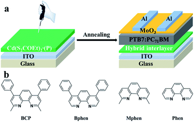 | ||
| Fig. 1 (a) Device structure of the inverted OSCs fabricated with different CdS–P hybrid interlayers, and (b) the molecular structures of BCP, Bphen, Mphen and Phen. | ||
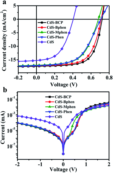 | ||
Fig. 2 (a) Illuminated and (b) dark J–V characteristic curves of devices, with the architecture of ITO/interlayer/PTB7![[thin space (1/6-em)]](https://www.rsc.org/images/entities/char_2009.gif) : :![[thin space (1/6-em)]](https://www.rsc.org/images/entities/char_2009.gif) PC71BM/MoO3/Al and with hybrid CdS–P or pure CdS as the interlayer. PC71BM/MoO3/Al and with hybrid CdS–P or pure CdS as the interlayer. | ||
| Interlayer | V oc V | J sc mA cm−2 | FF % | PCE | R s Ω cm2 | R sh kΩ cm2 |
|---|---|---|---|---|---|---|
| Best(Avg) | ||||||
| CdS–BCP | 0.722 | 17.42 | 66.44 | 8.36(8.23) | 4.21 | 1.04 |
| CdS–Bphen | 0.711 | 17.23 | 64.02 | 7.84(7.72) | 6.17 | 2.23 |
| CdS–Mphen | 0.681 | 16.98 | 57.86 | 6.69(6.55) | 9.30 | 0.85 |
| CdS–Phen | 0.707 | 17.19 | 54.08 | 6.57(6.49) | 14.74 | 0.88 |
| CdS | 0.404 | 15.27 | 50.13 | 3.09(2.96) | 7.43 | 0.31 |
Fig. 2b presents the dark J–V curves of the devices. With hybrid interlayers, the devices exhibit a turn-on voltage of about 0.7–0.8 V while it is only 0.5–0.6 V for the CdS interlayer device, suggesting the built-in potential across the device, which is the upper limit of the attainable Voc in OSCs,32 and considerably increases upon utilization of the hybrid cathode interlayers. In addition, the leakage current in the devices with hybrid interlayers is significantly restrained, and the diode rectification ratio characterized at ±2.0 V is 2–3 orders higher than that of the control device, indicating a greatly suppressed carrier recombination.33 Obviously, hole blocking and electron collecting become more efficient when the hybrid CdS–P cathode buffer layers are used. Thus, higher photocurrent is accomplished by using hybrid interlayers. Furthermore, the hybrid interlayer devices show a higher EQE value on average than the CdS based device in the wavelength range between 350 and 700 nm (Fig. S4†), which could have been resulted from the more efficient electron transport and collection at the electrode after modification of the CdS by organic ligands, since no obvious contribution derived from interlayer absorption to the photocurrent is observed as demonstrated by the absorption spectra of devices with the CdS–BCP or CdS interlayer (Fig. S5†).
To evaluate the charge carrier mobility in the devices incorporated with the hybrid interlayers CdS–P, the apparent charge transport mobilities were tested by using electron-only devices with the structure of ITO/CdS or CdS–P/PTB7![[thin space (1/6-em)]](https://www.rsc.org/images/entities/char_2009.gif) :
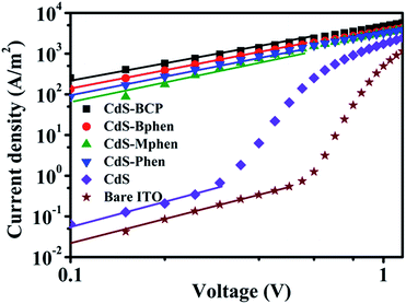
:![[thin space (1/6-em)]](https://www.rsc.org/images/entities/char_2009.gif) PC71BM/LiF/Al (Fig. S6†), according to the space charge limited current (SCLC) model (Fig. 3).25,32,34 As fitted by the SCLC model, apparent electron mobilities are determined to be 3.42 × 10⁻³, 2.58 × 10⁻³, 1.37 × 10⁻³, 1.80 × 10⁻³ cm2 V−1 s−1 for CdS–BCP, CdS–Bphen, CdS–Mphen, and CdS–Phen based devices, which are three orders of magnitude higher compared to that of the pristine CdS interlayer devices (1.61 × 10⁻⁶ cm2 V−1 s−1). And this enhanced charge carrier mobility could account for the Jsc improvement of the hybrid interlayer based devices compared to the CdS based device.
PC71BM/LiF/Al (Fig. S6†), according to the space charge limited current (SCLC) model (Fig. 3).25,32,34 As fitted by the SCLC model, apparent electron mobilities are determined to be 3.42 × 10⁻³, 2.58 × 10⁻³, 1.37 × 10⁻³, 1.80 × 10⁻³ cm2 V−1 s−1 for CdS–BCP, CdS–Bphen, CdS–Mphen, and CdS–Phen based devices, which are three orders of magnitude higher compared to that of the pristine CdS interlayer devices (1.61 × 10⁻⁶ cm2 V−1 s−1). And this enhanced charge carrier mobility could account for the Jsc improvement of the hybrid interlayer based devices compared to the CdS based device.
In addition, the surface morphologies of CdS and different hybrid interfacial films were investigated by SEM, as displayed in Fig. 4. The CdS film presents an island shaped morphology when deposited on a bare ITO substrate as shown in Fig. 4e, while the BCP and Bphen modified CdS films show dense black dots (in the scale of 10 μm) well distributed on the surface of ITO (Fig. 4a and b), and the CdS–Mphen and CdS–Phen films show a reticulated surface morphology on ITO (Fig. 4c and d), all of which are distinct from the pure CdS film. The difference in the surface morphology of the different hybrid CdS–P films could partly explain the different improvement of their performance,35–37 indicating that these hybrid CdS–P films can play an important role in delivering a high device performance. Furthermore, we conducted the AFM test in a tapping mode for the photoactive layer (PTB7![[thin space (1/6-em)]](https://www.rsc.org/images/entities/char_2009.gif) :
:![[thin space (1/6-em)]](https://www.rsc.org/images/entities/char_2009.gif) PC71BM) on different hybrid interlayers (Fig. S7†). The PTB7
PC71BM) on different hybrid interlayers (Fig. S7†). The PTB7![[thin space (1/6-em)]](https://www.rsc.org/images/entities/char_2009.gif) :
:![[thin space (1/6-em)]](https://www.rsc.org/images/entities/char_2009.gif) PC71BM films on top of CdS–BCP, CdS–Bphen and CdS–Phen hybrid interlayers exhibit a similar smoother surface and better phase separation compared to the active layer on the CdS film, which is consistent with the obtained device performances.
PC71BM films on top of CdS–BCP, CdS–Bphen and CdS–Phen hybrid interlayers exhibit a similar smoother surface and better phase separation compared to the active layer on the CdS film, which is consistent with the obtained device performances.
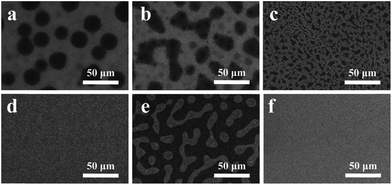 | ||
| Fig. 4 SEM images of different hybrid cathode interlayer coated ITOs. (a) CdS–BCP, (b) CdS–Bphen, (c) CdS–Mphen, (d) CdS–Phen, (e) CdS, and (f) bare ITO. | ||
Aggregates of the hybrid materials deposited on the ITO substrate are considered to be chelate compounds i.e. CdS–BCP, CdS–Bphen, CdS–Mphen and CdS–Phen, in which CdS is still coordinating with BCP, Bphen, Mphen and Phen, respectively, when decomposed from their precursors at 175 °C. As BCP (/Bphen/Mphen/Phen) is a bidentate ligand and two nitrogen atoms of which can bond to the Cd atom, the hydrophilic nature of the CdS film is thence changed after modification by different organic ligands (Fig. 5). In the hybrid films, nitrogen atoms possess higher electronegativity and thus chelate the CdS closely while the aromatic ring will orient upwards due to its lower electronegativity, which makes the film hydrophobic and compatible with nonpolar chlorobenzene solvent. This is consistent with the results of the water contact angle measurements (Fig. 5). In particular, in the films of CdS–BCP and CdS–Bphen (Fig. 5a and b), the existence of the diphenyl group makes them more hydrophobic than the CdS–Mphen and CdS–Phen (Fig. 5c and d).34 The bare ITO with a contact angle of 12° is displayed in Fig. 5f for comparison. The water contact angle increases from 54° of the pristine CdS to 78°, 76°, 60° and 66° of the CdS–BCP, CdS–Bphen, CdS–Mphen and CdS–Phen films, respectively. The results confirm the more hydrophobic property of the hybrid CdS–P surfaces, which is consistent with the results of the SEM analysis. In brief, these hybrid interfacial layers obtained by organic ligand modification can increase the interfacial intimate contact with the photoactive layer, benefiting the device performance.
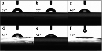 | ||
| Fig. 5 Water contact angle images of (a) CdS–BCP 78°, (b) CdS–Bphen 76°, (c) CdS–Mphen 60°, (d) CdS–Phen 66°, (e) CdS 54° and (f) bare ITO 12°. | ||
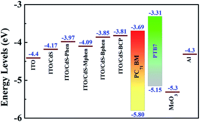
Moreover, for high performance OSCs, well-matched energy levels between the CdS–P interlayer modified electrode and the photoactive layer are required. Fig. 6 shows the energy level diagrams of the materials used in this work according to the studies of the UPS measurement (Fig. S8†) and reported scientific literature studies.38,39 The work function of bare ITO is measured to be −4.4 eV while the LUMO of PC71BM is −3.69 eV. After modification by CdS or hybrid CdS–P, the work functions are effectively decreased to −4.17 eV and −3.97, −4.09, −3.85, −3.81 eV, respectively, due to the introduced different electronic dipoles by their different molecule polarities,35,40,41 which are more comparable to the LUMO of PC71BM. Hence, electrons can be more facilely transferred from the LUMO of PC71BM to the ITO electrode through the interlayers and collected more efficiently. Furthermore, the Voc of devices fabricated with CdS or hybrid CdS–P interlayers would be related to the variation of their work functions. However, the Voc can also be influenced by the different work functions of the two electrodes when the interfaces between the active layer and electrodes are non-ohmic contacts.42,43 In our study, the Voc of the inverted solar cells is dependent on the work functions of the cathode interlayers. The decreased effective work functions of hybrid cathode buffer layers can lead to larger build-in potentials, and they are the upper limits of the attainable Voc in devices as described above. Therefore, the Voc of devices based on CdS–BCP, CdS–Bphen, CdS–Mphen and CdS–Phen interlayers increases to 0.722, 0.711, 0.681 and 0.707 V, respectively, compared to 0.404 V of the CdS-based device. The decreased effective work functions of CdS–P films may be attributed to the fill-up of CdS surface traps by phenanthroline and its derivatives, which would greatly decrease the possible trap-assisted interfacial charge recombination. In addition, the energy-level adjustment using hybrid CdS–P interlayers becomes more facile for electron extraction, which is consistent with a large forward current and a large photocurrent and can explain the trend of Jsc, eventually leading to high performance of OSCs.
Conclusions
In summary, we fabricated inverted organic solar cells by using homologous hybrid materials CdS–BCP, CdS–Bphen, CdS–Mphen and CdS–Phen as electron transporting layers. A high polarity and boiling point solvent, DMF, is selected to process the hybrid interfacial layers as it is able to improve the interface properties and enhance device performance. The influences of different organic ligands (BCP, Bphen, Mphen, Phen) on the performance of the inverted OSCs were investigated comprehensively. Modification of the CdS with organic ligands, effectively improved the electron mobility, film morphology, interfacial contact, and energy alignment, eventually leading to enormous enhancement of device performance, with PCE improved from 3.09% to 8.36, 7.84, 6.69, 6.57%, respectively. And the hybrid interlayers with the hydrophobic diphenyl group (CdS–BCP and CdS–Bphen) is favorable to fabricate high performance devices. These results indicate that the strategy of hybridization of conventional inorganic and organic semiconductors could produce promising charge carrier transporting materials for organic optoelectronic devices.Acknowledgements
The Project was supported by the National Natural Science Foundation of China (51273208, 61474125, 51502313), and Zhejiang Provincial Natural Science Foundation of China (LR14E030002) and Ningbo City Natural Science Foundation of China (2014A610037). The work was also supported by the Hundred Talent Program of Chinese Academy of Sciences. We also thank the support from the Jiangsu Collaborative Innovation Center of Photovoltaic Science and Engineering (Changzhou, 213164, P. R. China).Notes and references
- G. Li, R. Zhu and Y. Yang, Nat. Photonics, 2012, 6, 153–161 CrossRef CAS.
- B. C. Thompson and J. M. J. Fréchet, Angew. Chem., Int. Ed., 2008, 47, 58–77 CrossRef CAS PubMed.
- L. Ye, S. Zhang, L. Huo, M. Zhang and J. Hou, Acc. Chem. Res., 2014, 47, 1595–1603 CrossRef CAS PubMed.
- Z. He, B. Xiao, F. Liu, H. Wu, Y. Yang, S. Xiao, C. Wang, T. P. Russell and Y. Cao, Nat. Photonics, 2015, 9, 174–179 CrossRef CAS.
- L. K. Jagadamma, M. Al-Senani, A. El-Labban, I. Gereige, N. Ndjawa, O. Guy, J. C. Faria, T. Kim, K. Zhao and F. Cruciani, Adv. Energy Mater., 2015, 5, 1500204 Search PubMed.
- S. Zhang, L. Ye, W. Zhao, B. Yang, Q. Wang and J. Hou, Sci. China: Chem., 2015, 58, 248–256 CrossRef CAS.
- J. Kong, I. W. Hwang and K. Lee, Adv. Mater., 2014, 26, 6275–6283 CrossRef CAS PubMed.
- Y. Liu, J. Zhao, Z. Li, C. Mu, W. Ma, H. Hu, K. Jiang, H. Lin, H. Ade and H. Yan, Nat. Commun., 2014, 5, 5293 CrossRef CAS PubMed.
- C.-C. Chueh, C.-Z. Li and A. K.-Y. Jen, Energy Environ. Sci., 2015, 8, 1160–1189 CAS.
- Z. He, C. Zhong, S. Su, M. Xu, H. Wu and Y. Cao, Nat. Photonics, 2012, 6, 591–595 Search PubMed.
- R. Xia, D. S. Leem, T. Kirchartz, S. Spencer, C. Murphy, Z. He, H. Wu, S. Su, Y. Cao and J. S. Kim, Adv. Energy Mater., 2013, 3, 718–723 CrossRef CAS.
- W. E. Ford, D. Gao, N. Knorr, R. Wirtz, F. Scholz, Z. Karipidou, K. Ogasawara, S. Rosselli, V. Rodin and G. Nelles, ACS Nano, 2014, 8, 9173–9180 CrossRef CAS PubMed.
- T. M. Clarke and J. R. Durrant, Chem. Rev., 2010, 110, 6736–6767 CrossRef CAS PubMed.
- A. Hadipour, D. Cheyns, P. Heremans and B. P. Rand, Adv. Energy Mater., 2011, 1, 930–935 CrossRef CAS.
- A. K. K. Kyaw, D. H. Wang, D. Wynands, J. Zhang, T.-Q. Nguyen, G. C. Bazan and A. J. Heeger, Nano Lett., 2013, 13, 3796–3801 CrossRef CAS PubMed.
- J. H. Seo, A. Gutacker, Y. Sun, H. Wu, F. Huang, Y. Cao, U. Scherf, A. J. Heeger and G. C. Bazan, J. Am. Chem. Soc., 2011, 133, 8416–8419 CrossRef CAS PubMed.
- Y. Sun, S.-C. Chien, H.-L. Yip, Y. Zhang, K.-S. Chen, D. F. Zeigler, F.-C. Chen, B. Lin and A. K.-Y. Jen, Chem. Mater., 2011, 23, 5006–5015 CrossRef CAS.
- W. Zhang, Y. Wu, Q. Bao, F. Gao and J. Fang, Adv. Energy Mater., 2014, 4, 1400359 Search PubMed.
- Z. a. Tan, W. Zhang, Z. Zhang, D. Qian, Y. Huang, J. Hou and Y. Li, Adv. Mater., 2012, 24, 1476–1481 CrossRef CAS PubMed.
- Y. Sun, J. H. Seo, C. J. Takacs, J. Seifter and A. J. Heeger, Adv. Mater., 2011, 23, 1679–1683 CrossRef CAS PubMed.
- M. D. Irwin, D. B. Buchholz, A. W. Hains, R. P. Chang and T. J. Marks, Proc. Natl. Acad. Sci. U. S. A., 2008, 105, 2783–2787 CrossRef CAS.
- T. Stubhan, M. Salinas, A. Ebel, F. C. Krebs, A. Hirsch, M. Halik and C. J. Brabec, Adv. Energy Mater., 2012, 2, 532–535 CrossRef CAS.
- H. Choi, J. S. Park, E. Jeong, G. H. Kim, B. R. Lee, S. O. Kim, M. H. Song, H. Y. Woo and J. Y. Kim, Adv. Mater., 2011, 23, 2759–2763 CrossRef CAS PubMed.
- Y. Zhou, C. Fuentes-Hernandez, J. Shim, J. Meyer, A. J. Giordano, H. Li, P. Winget, T. Papadopoulos, H. Cheun and J. Kim, Science, 2012, 336, 327–332 CrossRef CAS PubMed.
- S. H. Liao, H. J. Jhuo, Y. S. Cheng and S. A. Chen, Adv. Mater., 2013, 25, 4766–4771 CrossRef CAS PubMed.
- S.-H. Liao, H.-J. Jhuo, P.-N. Yeh, Y.-S. Cheng, Y.-L. Li, Y.-H. Lee, S. Sharma and S.-A. Chen, Sci. Rep., 2014, 4, 6813 CrossRef CAS PubMed.
- J. Liu, J. Wu, S. Shao, Y. Deng, B. Meng, Z. Xie, Y. Geng, L. Wang and F. Zhang, ACS Appl. Mater. Interfaces, 2014, 6, 8237–8245 CAS.
- Y. Wu, W. Zhang, X. Li, C. Min, T. Jiu, Y. Zhu, N. Dai and J. Fang, ACS Appl. Mater. Interfaces, 2013, 5, 10428–10432 CAS.
- L. Zuo, Z. Gu, T. Ye, W. Fu, G. Wu, H. Li and H. Chen, J. Am. Chem. Soc., 2015, 137, 2674–2679 CrossRef CAS PubMed.
- W. Chen, Y. Wu, J. Liu, C. Qin, X. Yang, A. Islam, Y.-B. Cheng and L. Han, Energy Environ. Sci., 2015, 8, 629–640 CAS.
- V. Varand, L. Glinskaya, R. Klevtsova and S. Larionov, J. Struct. Chem., 1998, 39, 244–252 CrossRef CAS.
- Z. He, C. Zhong, X. Huang, W. Y. Wong, H. Wu, L. Chen, S. Su and Y. Cao, Adv. Mater., 2011, 23, 4636–4643 CrossRef CAS PubMed.
- V. Mihailetchi, P. Blom, J. Hummelen and M. Rispens, J. Appl. Phys., 2003, 94, 6849–6854 CrossRef CAS.
- B. R. Lee, E. D. Jung, Y. S. Nam, M. Jung, J. S. Park, S. Lee, H. Choi, S. J. Ko, N. R. Shin and Y. K. Kim, Adv. Mater., 2014, 26, 494–500 CrossRef CAS PubMed.
- A. Kahn, Mater. Horiz., 2015 10.1039/c5mh00160a.
- R. Steim, F. R. Kogler and C. J. Brabec, J. Mater. Chem., 2010, 20, 2499–2512 RSC.
- M. Gräetzel, R. A. Janssen, D. B. Mitzi and E. H. Sargent, Nature, 2012, 488, 304–312 CrossRef PubMed.
- C. Tao, S. Ruan, X. Zhang, G. Xie, L. Shen, X. Kong, W. Dong, C. Liu and W. Chen, Appl. Phys. Lett., 2008, 93, 193307 CrossRef.
- Y. Liang, Z. Xu, J. Xia, S. T. Tsai, Y. Wu, G. Li, C. Ray and L. Yu, Adv. Mater., 2010, 22, E135–E138 CrossRef CAS PubMed.
- R. T. Tung, Phys. Rev. B: Condens. Matter Mater. Phys., 2001, 64, 205310 CrossRef.
- X. Crispin, V. Geskin, A. Crispin, J. Cornil, R. Lazzaroni, W. R. Salaneck and J.-L. Bredas, J. Am. Chem. Soc., 2002, 124, 8131–8141 CrossRef CAS PubMed.
- J. Liu, S. Shao, G. Fang, B. Meng, Z. Xie and L. Wang, Adv. Mater., 2012, 24, 2774–2779 CrossRef CAS PubMed.
- H.-H. Liao, L.-M. Chen, Z. Xu, G. Li and Y. Yang, Appl. Phys. Lett., 2008, 92, 173303 CrossRef.
Footnotes |
† Electronic supplementary information (ESI) available: Details of the XPS spectra of CdS and CdS–BCP, J–V characteristics of OSCs based on various solvents with different concentrations, AFM height images of CdS–BCP with different solvents, EQE, absorption spectra, characteristic curves of electron-only devices, AFM height images of PTB7![[thin space (1/6-em)]](https://www.rsc.org/images/entities/char_2009.gif) : :![[thin space (1/6-em)]](https://www.rsc.org/images/entities/char_2009.gif) PC71BM and UPS spectra. See DOI: 10.1039/c5ta06952a PC71BM and UPS spectra. See DOI: 10.1039/c5ta06952a |
| ‡ Xiaohui Liu and Yulei Wu contributed equally to this work. |
| This journal is © The Royal Society of Chemistry 2016 |

