
Tubular structures from the LnS–TaS2 (Ln = La, Ce, Nd, Ho, Er) and LaSe–TaSe2 misfit layered compounds†
Gal
Radovsky
a,
Ronit
Popovitz-Biro
b,
Tommy
Lorenz
c,
Jan-Ole
Joswig
c,
Gotthard
Seifert
c,
Lothar
Houben
d,
Rafal E.
Dunin-Borkowski
d and
Reshef
Tenne
*a
aDepartment of Materials and Interfaces, Weizmann Institute of Science, Rehovot 76100, Israel. E-mail: Reshef.Tenne@weizmann.ac.il; Fax: +972-8-934-4138; Tel: +972-8-934-2394
bChemical Research Support, Weizmann Institute of Science, Rehovot 76100, Israel
cPhysikalische Chemie, Technische Universität Dresden, Bergstr. 66b, D-01069 Dresden, Germany
dErnst Ruska-Centre for Microscopy and Spectroscopy with Electrons and Peter Grünberg Institute, Forschungszentrum Jülich, D-52425 Jülich, Germany
First published on 23rd October 2015
Abstract
Nanotubular structures from a new family of misfit compounds LnS–TaS2 with (Ln = La, Ce, Nd, Ho, Er) and LaSe–TaSe2 (some of them not known hitherto) are reported. Stress relaxation originating from the lattice mismatch between the alternating LnS(Se) and TaS2(Se) layers, combined with seaming of the dangling bonds in the rim, leads to the formation of a variety of nanotubular structures. Their structures are studied via scanning electron microscopy (SEM), high-resolution transmission electron microscopy (HRTEM), scanning transmission electron microscopy (STEM) and selected area electron diffraction (SAED). Tubules exhibiting a single folding vector for the LnS(Se) as well as TaS2(Se) layers were often found. The small values of the c-axis periodicities are indicative of a strong interaction between the two constituent layers which was also supported by Raman spectroscopy and theoretical calculations.
Introduction
Misfit layered compounds
Misfit layered compounds (MLC) have a general formula of (MX)1+y(TX2)m with (M = Sn, Pb, Sb, Bi, rare earths; T = Nb, Ta, Ti, V, Cr; X = S, Se; 0.08 ≤ y ≤ 0.28; m = 1–3).1,2 The TX2 and MX layers have different crystallographic structure and they are stacked periodically. TX2 is a three-atom thick sandwich layer with a pseudo-hexagonal structure, in which the metal atoms are surrounded by six chalcogen atoms, either in octahedral or in trigonal prismatic coordination. Although bulk TaS2 can adopt either structure,3–6 trigonal prismatic is the relevant coordination in MLC.1,2,7 The two atom thick MX slice can be considered as a distorted NaCl structure with an orthorhombic unit cell. The value of y is determined by the ratio of the projected atomic surface densities of the two subsystems. Interactions between the MX and TX2 subsystems result in various types of mutual structural modulations, depending on the compounds.1,2,7 For the LnS–TaS2 and LaSe–TaSe2 MLC that are discussed here, the mutual structural modulation results in an in-plane commensurate “b” and an in-plane incommensurate “a” direction. In particular, the b-axis of LnS (Fig. 1a) fits to √3 × a of TaS2, where a is the in-plane lattice parameter of TaS2 when indexed according to a pseudohexagonal unit cell (marked in brown in Fig. 1b). Therefore, it is convenient to describe the pseudohexagonal TaS2 layer in terms of an ortho-pseudohexagonal unit cell that has primitive dimensions a and b = √3 × a, as shown in purple in Fig. 1b. A misfit then occurs along the a direction, as the ratio aLnS/aTaS2 is an irrational number. Therefore, the superstructure lacks three dimensional periodicity and it is impossible to define one common unit cell. A complete description of the entire structure is possible in a (3 + 1)D superspace1,2 where an additional dimension (D) is inserted to reflect the incommensurate modulation of the atomic positions of the two subsystems along the a-axis. | ||
| Fig. 1 Schematic model showing the stacking and the relative in-plane orientation of the TaX2 and the LnX (X = S, Se) layers in many of the tubular structures from the LnX–TaX2 MLC. (a) Single layer of LnX projected along the c-axis and oriented in such a way that its b-axis is parallel to the tubule axis (blue arrow) and to the solid green arrow in (b). (b) Single layer of TaX2 projected along the c-axis. Pseudohexagonal and ortho-pseudohexagonal unit cells are marked in brown and purple respectively. The solid green arrow represents the b-axis with respect to the ortho-pseudohexagonal unit cell, coincides with the tube axis (blue arrow). The two dashed green arrows represent crystallographically equivalent directions rotated by 60° and 120° relative to the direction marked by the solid green arrow. (c) Initiation of bending around the b-axes of the LnX and TaX2 layers that comprise an LnX–TaX2 slab. (d) A concentric tubule whose axis (perpendicular to the plane of the paper) coincides with the b-axes of LnX and TaX2. (e) Representative partially unfolded sheets, demonstrating the scrolling process for the NdS–TaS2 MLC case in particular. | ||
It should be noticed that some of the compounds described in the present study, like HoS–TaS2 and LaSe–TaSe2, were not reported in the literature before even in the bulk form.
Stability of LnS–TaS2 misfit compounds
The Ln atoms within LnS–TaS2 MLC inherently prefer a trivalent state.1,8 It has been proposed that a considerable amount of charge transfer from LnS to the partially filled TaS2 dz2 band8–10 enhances the Coulombic interaction between the two sublayers which is believed to be one of the stabilizing mechanisms of these compounds. The dz2 band is a very narrow (∼1 eV wide) band formed by the hybridization of dz2 and dx2−y2 Ta orbitals and is half full in 2H–TaS2.8–10The larger amount of charge transfer may result in higher Coulombic interaction between the LnS and the TaS2 layers, shorter bond lengths between the Ln and the S atoms of the TaS2 layer8 and smaller periodicity values along the c-axis.
Magnetic and electrical properties of the bulk materials
As a result of the magnetic moment of the two atom thick LnS layers, bulk LnS–TaS2 MLC have been found to exhibit interesting magnetic properties.1,10 For example, it was shown that when Ln = Ce, Gd and Dy the magnetic susceptibility shows a maximum at 2.7, 4.1 and 1.7 K, respectively. This observation was attributed to low temperature antiferromagnetic ordering.10 However, when Ln = Nd, Er, the susceptibility obeyed the Curie–Weiss law and showed no magnetic transition down to 1.2 K (the lowest temperature investigated in these studies).10 LaS–TaS2 has been found to be diamagnetic.10 Bulk LnS–TaS2 MLC have a metallic temperature dependence of their electrical conduction.1,8,10 However, in contrast to MS–TaS2 (with M = Sn, Pb, Bi, Sb)11,12 MLC, no superconducting transitions have been reported for these compounds.Nanotubes from the LnS–TaS2 MLC exhibit unique structural characteristics not described hitherto, and potentially have interesting magnetic and electrical properties. However, magnetic and electrical measurements are time consuming and will be the scope of future publications.
Formation of tubular structures
The misfit in the a–b plane is the main driving force for scrolling as shown in Fig. 1c. In the MLC discussed here, such a misfit occurs along the a-axis. The tubule axis is then expected to be parallel to the common b-axis and perpendicular to the a-axis along which the lattice parameters differ most as shown in Fig. 1a.Upon scrolling, the energy associated with the misfit is reduced.13 Spontaneous bending is mostly expected for an asymmetric MX–TX2 lamella, i.e. one that is bounded by MX on one side and by TX2 on the opposite side. The formation of the nanotubes is further stimulated by the seaming of dangling bonds at the rims of the layers as reported before for binary layered compounds, like WS2, and is shown schematically in Fig. 1c. These two independent mechanisms promote the formation of concentric tubules which may effectively decrease the minimal equilibrium radius resulting from the misfit.
Experimental and computational section
Synthesis of the tubular structures
The synthesis of LnS–TaS2 (Ln = La, Ce, Nd, Ho, Er) and LaSe–TaSe2 MLC tubular structures was carried out in evacuated ampoules at a vacuum of ∼5 × 10⁻⁵ torr. Ta, Ln, S or Se powders were taken at molar ratios of ∼1![[thin space (1/6-em)]](https://www.rsc.org/images/entities/char_2009.gif) :1:3. Small amounts of TaCl5 or TaBr5 (∼0.1 of a molar amount of Ta) powder were added as a Cl/Br source. Cl/Br is believed to act as a transport agent. The powders used were purchased from the following companies and had the following purity: La, Ho, Er (Strem Chemicals 99.9%), Nd (Strem Chemicals 99.8%), Ce (Alfa Aesar 99.9%), Ta (Alfa Aesar 99.9%), S (Sigma Aldrich 99.98%), Se (Fluka 99.9%), TaCl5 (Alfa Aesar 99.8%), TaBr5 (Strem Chemicals 99.9%). The materials were inserted into the ampoule in a glove box at a nitrogen atmosphere to prevent oxidation. After sealing, the ampoules were inserted into a preheated vertical furnace and two annealing steps were performed. First, the ampoules were held in a temperature gradient of 400 °C at the bottom (with the precursors) and 850 °C at the upper part for 1 h. In the second step, the temperatures were tuned to 850 °C at the bottom (with the precursors) and 50 °C at the upper part. This step lasted for 4–16 h. Afterwards the ampoules were removed rapidly from the furnace and were cooled at plain air. Most of the product remained at the hot edge of the ampoules and the amount of the substance transported to the cold edge was negligible. It should be emphasized that the nanotubes are obtained in appreciable yields under a narrow window of conditions, only. Otherwise, micron-size platelets of the same compounds or the binary compounds predominate in the reaction product.
:1:3. Small amounts of TaCl5 or TaBr5 (∼0.1 of a molar amount of Ta) powder were added as a Cl/Br source. Cl/Br is believed to act as a transport agent. The powders used were purchased from the following companies and had the following purity: La, Ho, Er (Strem Chemicals 99.9%), Nd (Strem Chemicals 99.8%), Ce (Alfa Aesar 99.9%), Ta (Alfa Aesar 99.9%), S (Sigma Aldrich 99.98%), Se (Fluka 99.9%), TaCl5 (Alfa Aesar 99.8%), TaBr5 (Strem Chemicals 99.9%). The materials were inserted into the ampoule in a glove box at a nitrogen atmosphere to prevent oxidation. After sealing, the ampoules were inserted into a preheated vertical furnace and two annealing steps were performed. First, the ampoules were held in a temperature gradient of 400 °C at the bottom (with the precursors) and 850 °C at the upper part for 1 h. In the second step, the temperatures were tuned to 850 °C at the bottom (with the precursors) and 50 °C at the upper part. This step lasted for 4–16 h. Afterwards the ampoules were removed rapidly from the furnace and were cooled at plain air. Most of the product remained at the hot edge of the ampoules and the amount of the substance transported to the cold edge was negligible. It should be emphasized that the nanotubes are obtained in appreciable yields under a narrow window of conditions, only. Otherwise, micron-size platelets of the same compounds or the binary compounds predominate in the reaction product.
Electron microscopy, XRD, Raman spectroscopy
After the ampoules were opened, the powder products from the hot zone were examined by SEM, HRTEM, STEM, XRD, and Raman spectroscopy.X-ray diffraction (XRD) patterns were recorded with a Rigaku TTRAXIII diffractometer (Cu-Kα radiation, 1.54 Å) operating in the Bragg–Brentano (θ–2θ) mode. For SEM analysis, a small amount of the powder was placed on carbon tape stuck to an aluminum stub. The resulting samples were examined using a Zeiss Ultra model V55 SEM and a LEO model Supra 55VP SEM equipped with an EDS detector (Oxford model INCA).
For high-resolution transmission electron microscopy (HRTEM) a solution of the product in ethanol was dripped onto a lacey/holey carbon/collodion-coated Cu grids. The resulting samples were examined by Philips CM120 TEM, operating at 120 kV equipped with EDS detector (EDAX-Phoenix Microanalyzer); JEOL JEM2100 operating at 200 kV and FEI Tecnai F30-UT HRTEM operating at 300 kV. High-resolution scanning transmission electron microscopy (STEM) images and EDS chemical maps were taken on a probe-corrected FEI Titan 80-200 G2 ChemiSTEM instrument equipped with a Bruker Super-X detector at 200 kV.
For Raman spectroscopy measurements, droplets of an ethanol solution containing the product were dripped on Si wafers. Raman measurements were carried out using a Renishaw Micro Raman InVia Imaging Microscope equipped with a CCD device. Tubes with diameters of 0.2–1 μm could easily be discerned using the light microscope. A He–Ne laser (λ = 633 nm) was used for excitation.
Computational details
The present calculations were based on the density-functional tight-binding (DFTB) method. For these calculations, rectangular periodic boundary conditions were applied. The effective one-electron potential in the Kohn–Sham Hamiltonian is approximated as a superposition of the potentials of the neutral atoms. Furthermore, only one- and two-center integrals are calculated to set-up a scalar relativistic Hamilton matrix. The valence basis included the 6s, 6p, and 5d orbitals for La; 3s and 3p orbitals for S and the 5s, 5p, and 4d orbitals for Ta. The states below these levels were treated within a frozen-core approximation. For a detailed description of the calculations, see Section S7.1 in the ESI.†Results and discussion
Here nanotubes from a new family of LnS–TaS2 (LaSe–TaSe2) MLC, are reported. The tubular phase constituted ∼50% of the total product for the LaS–TaS2 case, ∼20% for NdS–TaS2 and ErS–TaS2, ∼5% for HoS–TaS2 and LaSe–TaSe2 and merely 1% for the CeS–TaS2 case. Syntheses were carried out in fused silica tubes under vacuum. The tubular structures were produced in the hot zone of the ampoules among other by-products, in contrast to e.g. MS–TaS2 with M = Sn, Pb, Bi, Sb that condensed at the cold end of a temperature gradient.7 The addition of a small amount of TaCl5 or TaBr5 powders was essential for nanotube growth. The use of TaBr5 instead of TaCl5 resulted in a higher yield in the case of LaSe–TaSe2 nanotubes. For the sake of comparison, iodine was used as a transport agent for the growth of LnS–TaS2 MLC single crystals which were obtained at the cold zone of the tube within several days. Also, the ampoules were subjected to a very fine temperature gradient of 850–950 °C between the edges.10 Typically, a deviation of only a few degrees from the prescribed procedure leads to an appreciably smaller yield of the nanotubes in the product.Chemical analysis of the LnS–TaS2 with (Ln = La, Ce, Nd) tubular structures using both EDS within the SEM and TEM (of individual nanotubes) indicated the presence of 1–2 at% of Cl or Br in the case of LaSe–TaSe2. Indeed, peaks of Cl (Br) are clearly seen on the EDS spectra recorded from these compounds as shown in Fig. S2 in the ESI.† However, no clear peak of Cl could be detected for (Ln = Ho and Er). Nevertheless, in all cases (of LnS–TaS2 with Ln = La, Ce, Nd, Ho, Er and LaSe–TaSe2) tubular structures could not be produced without the addition of TaCl5 (TaBr5) powder to the ampoules.
Representative SEM images of the products are shown in Fig. 2 and Fig. S3 in the ESI.†
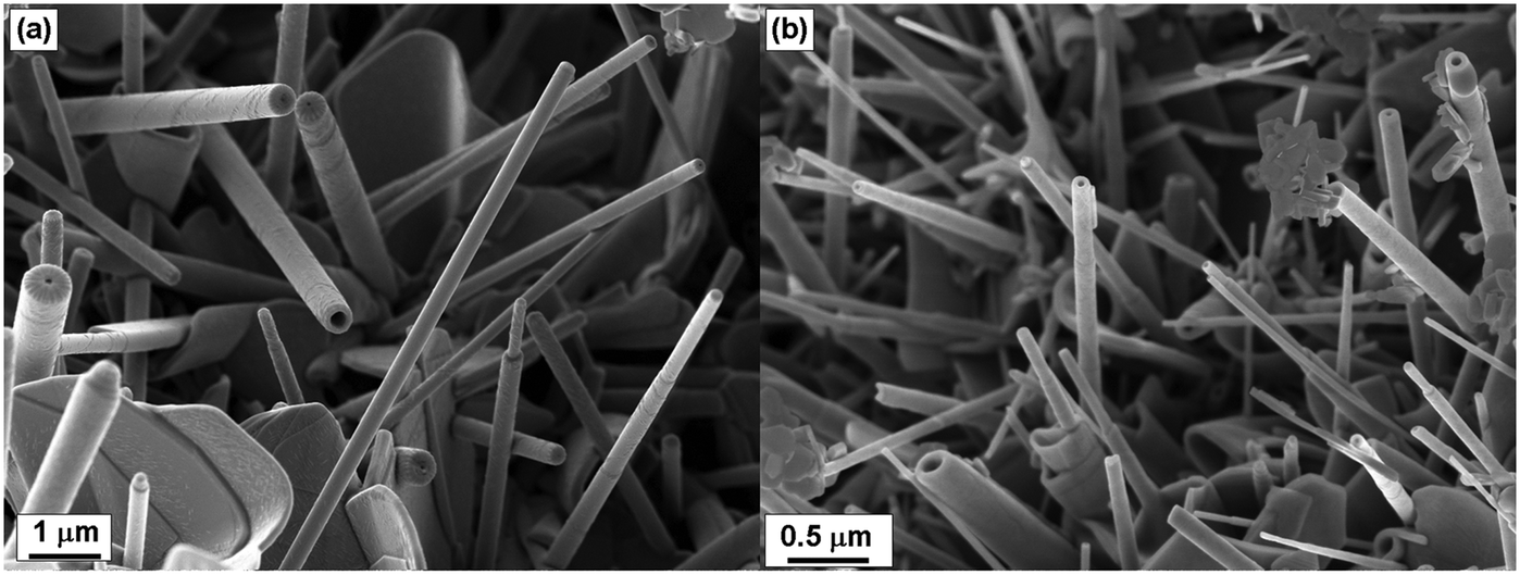 | ||
| Fig. 2 SEM images of the tubular structures and common by-products from (a) LaS–TaS2, (b) ErS–TaS2 MLC. Scrolling steps are visible at the significant part of the tubular crystals. | ||
Table 1 summarizes the typical range of outer diameters of the tubules as well as their yields of production.
| Compound | Yield [%] | Outer diameter [nm] |
|---|---|---|
| LaS–TaS2 | 50 | 40–1000 |
| CeS–TaS2 | 1 | 60–1000 |
| NdS–TaS2 | 20 | 130–1200 |
| HoS–TaS2 | 5 | 45–300 |
| ErS–TaS2 | 20 | 35–300 |
| LaSe–TaSe2 | 5 | 85–1000 |
The ratio between the inner and outer diameters varied between the limiting cases of 0 and 1 for all of the LnS(Se)–TaS2(Se) MLC tubular structures that are described here. Partially unrolled LnS–TaS2 MLC sheets, as well as pristine TaS2, LnS, and metallic Ln and Ta residuals (identified from XRD spectra; see Fig. 5 and Section S4 in the ESI†) were always present in the powder. It is suggested that in several cases after the initial tube is produced, further layers can form within the preformed core which serves as an “internal template”. Presumably also, the growth of the nanotubes did not start at once with some nanotubes starting to grow earlier and others later-on. Hence some of the nanotubes stayed longer in the reaction zone giving rise to the possibility for a secondary growth (templating effect) on the outer as well as the inner-most surface layer of the nanotube. Therefore, nanotubes of different internal and external diameters and length were obtained. That might explain the large variety of the internal diameters within the tubes. Furthermore, the seaming of the dangling bonds provides additional driving force for the formation of concentric tubes with small internal diameter. Energy-wise, templated growth is not as demanding and may lead to scrolling, as is often observed for the outermost layers of the tubular structures. Therefore, in such cases part of the layers have a tube-like morphology and part (mostly the outermost layers) show a scroll like structure.
Structural analysis of the tubular structures
In many of the tubules from all of the LnS(Se)–TaS2(Se) MLC that are discussed here, the classical behavior of one common b-axis coinciding with the tubule axis (as presented in Fig. 1) was observed. In this case both the TaS2(Se) and the LnS(Se) layers had a single folding vector. Tubules exhibiting two folding vectors of the TaS2 layers with one two or three folding vectors of the LnS layers were encountered as well (see Section S1.1 in the ESI†). The latter configuration of the layers is very common in nanotubes from the PbS–NbS214 and PbS–TaS27 MLC which were widely described by us in the past.TEM images of LnS–TaS2 with (Ln = La, Ce, Nd, Ho, Er) and LaSe2–TaSe2 tubular structures are shown in Fig. 3 and Fig. S5–S8 in the ESI.† The SAED patterns of the shown tubular structures indicate that there is a single folding vector for both the TaS2(Se) and the LnS(Se) layers, consistent with the structure shown in Fig. 1d. Such patterns were commonly encountered for LnS–TaS2 (Ln = La, Er) as shown in Fig. 3a and b and more rarely for (Ln = Ce, Nd, Ho) and LaSe–TaSe2 as shown in Fig. S7a, S6a, S6b and S5, respectively, in the ESI.†Fig. 3a shows the structure of a LaS–TaS2 nanotube. Here, the LaS and TaS2 layers are stacked in an alternating sequence along their common c-axis with a 1.15 nm periodicity, as determined from line profiles and from the distance between basal reflections in diffraction patterns. In Fig. 3a, six pairs of spots with interplanar spacings of 1.64 Å and 2.83 Å are equally-azimuthally distributed on a circle and are marked by small red circles. These spots are attributed to the (11.0) and (10.0) planes of TaS2 ((200) and (020) in the ortho-pseudohexagonal indexing system). The multiplicity factor for these planes is six.6 This observation suggests the presence of a single folding vector for the TaS2 layers. Four pairs of spots belonging to the LaS sublattice with interplanar spacings of 3.99 Å and 2.01 Å are marked by small green circles and attributed to the (110) and second order (220) reflections. The multiplicity factor for these planes is four,15 indicating that there is also a single folding vector for the LaS layers in this tube. The splitting of the hk.0 (of TaS2(Se)) and hk0 (of LnS(Se)) diffraction spots indicates a small chiral angle for both of the layers (see Section S1.2 in the ESI†). In the tubules analyzed here, the chiral angles of the TaS2(Se) and LnS(Se) within the same tubule are equal along the entire length of the nanotube, which attests to its crystalline quality. The values of the chiral angles are indicated in the figure captions.
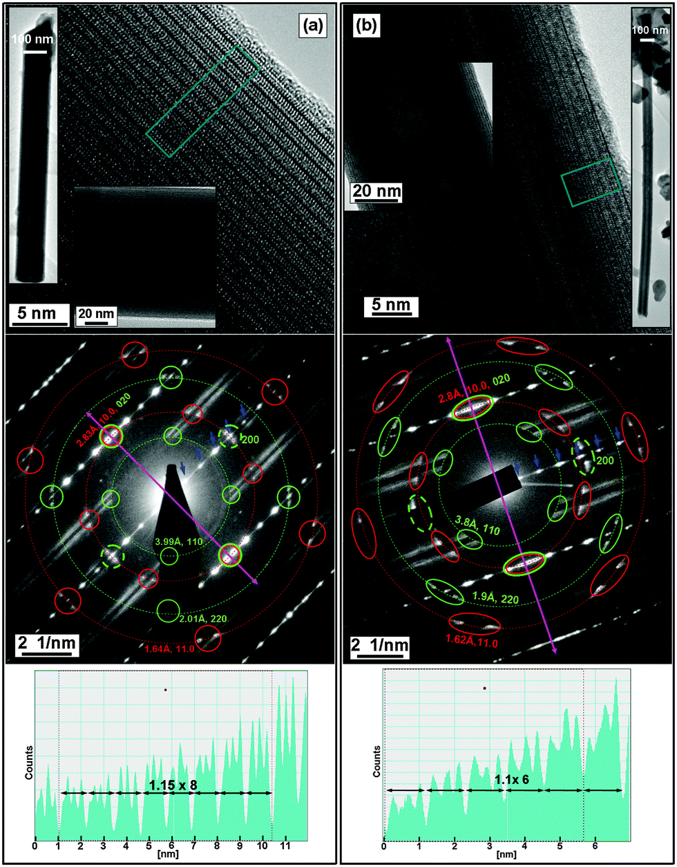 | ||
| Fig. 3 TEM images of (a) LaS–TaS2 and (b) ErS–TaS2 tubular crystals, with the LnS and TaS2 layers stacked periodically. Top: High magnification images, with medium and low magnification images shown as insets. Middle: SAED patterns acquired from the areas shown in the upper images. Spots corresponding to the same interplanar spacings are marked by large segmented ellipses or circles (red for TaS2 and green for LnS) and the respective Miller indices are indicated. The tubule axes are marked by purple double arrows. Basal reflections are marked by small blue arrows. Chiral angles of 3.1° and 7.2° for the tubules shown in (a) and (b), respectively, were determined from the splitting of the spots, as discussed in the text. Bottom: Line profiles perpendicular to the tubule axes integrated along the rectangles marked in the upper images. | ||
Two pairs of LaS 020 spots match the 10.0 spots of TaS2 (020 when indexed in the ortho-pseudohexagonal system) parallel to the tubule axis. These coincident spots (marked with both green and red small circles) reveal the presence of a common commensurate in-plane direction b that coincides with the nanotube axis, as expected and as shown in Fig. 1d. 200 LaS spots also appear and are marked by segmented small circles. As expected, these spots appear at azimuthal angles of 90° with respect to the 020 spots, which is equal to the angle between the (200) and (020) planes in orthorhombic LaS. The fact that the LaS 200 spots are approximately on the same circle as the 020 spots indicates that the a and b lattice parameters of LaS are almost equal. The first order LaS 010 and 100 spots are absent from the pattern, in agreement with previous observations.7,14
The SAED patterns of the LnS–TaS2 (Ln = Ce, Nd, Ho, Er) and LaSe–TaSe2, which are shown in Fig. S5, S6a, b, S7a (ESI†) and Fig. 3b, are similar to the pattern shown in Fig. 3a. However, the lattice periodicities of the latter MLC nanotubes are different from those of their LaS–TaS2 counterpart (see Table 2 and Section S5 in the ESI†). For example, in the ErS–TaS2 tubule shown in Fig. 3b, it is apparent that the 200 spots of ErS (marked by segmented green ellipses) are “shifted” slightly away from the red dashed circles that correspond to the 10.0 spots of TaS2 and the 020 spots of ErS. This shift is indicative of the presence of a slightly smaller interplanar a-spacing, when compared to the b-spacing of the ErS layer. Therefore, in this case the difference between the in-plane lattice parameters (a and b) of LnS (i.e., ErS) is more apparent. Such a shift is also apparent for HoS–TaS2 tubular structures (Fig. S6b, ESI†), but not for LaS–TaS2 (Fig. 3a), CeS–TaS2 (Fig. S7a, ESI†), NdS–TaS2 (Fig. S6a, ESI†) or LaSe–TaSe2 (Fig. S5, ESI†). Also, for the LaSe–TaSe2 tubule shown in Fig. S5 (ESI†), the lattice periodicities are significantly larger than for the LaS–TaS2 counterpart.
| Compound | TaS2d(11.0) = d(200)* = a/2 [Å] | TaS2d(10.0) = d(020)* = b/2 [Å] | LnS(110) [Å] | LnS(220) [Å] | LnS(200) = a/2 [Å] | LnS(020) = b/2 [Å] | Difference between a and b of LnS [%] | Mean c-axis periodicity ED/XRD [Å] | The value of y within (LnS)1+yTaS2 |
|---|---|---|---|---|---|---|---|---|---|
| LaS–TaS2 | 1.64 | 2.83 | 3.99 | 2.01 | 2.86 | 2.83 | 1 | 11.5/11.45 | 0.145 |
| CeS–TaS2 | 1.64 | 2.84 | 4.00 | 2.01 | 2.845 | 2.84 | 0.17 | 11.45 | 0.15 |
| NdS–TaS2 | 1.63 | 2.82 | 3.86 | 1.98 | 2.78 | 2.82 | 1.4 | 11.4/11.28 | 0.17 |
| HoS–TaS2 | 1.61 | 2.8 | 3.8 | 1.91 | 2.61 | 2.8 | 7.3 | 11.1 | 0.23 |
| ErS–TaS2 | 1.62 | 2.8 | 3.8 | 1.9 | 2.59 | 2.8 | 8 | 11.1/11.11 | 0.25 |
| LaSe–TaSe2 | 1.71 | 2.98 | 4.22 | 2.12 | 3.02 | 2.98 | 1.2 | 12 | 0.13 |
The in-plane lattice parameters (a and b) of LnS and TaS2 (labeled according to the ortho-pseudohexagonal system) were calculated from the 10.0 and 11.0 reflections of TaS2(Se) and from the 220 reflections of LnS(Se). The b-axis is commensurate and common to both the LnS and the TaS2 and was assumed to be equal for the calculations. The results are summarized in Table 2. The average stoichiometry of the tubes' constituents could be extracted from the lattice parameters of the TaS2(Se) and the LnS(Se) layers deduced from the SAED patterns. The approximate stoichiometries could be calculated from the ratio of the projected atomic surface densities of the two sublayers. The value of y within the LnS1+yTaS2 (or Se counterparts) can be calculated according to 2(aTaS2/aLnS) − 11 where the factor 2 represents the ratio of the number of formula units in the unit cell of each sublattice (4 for LnS(Se) and 2 for TaS2(Se)). These results are summarized in Table 2 as well and are comparable to the bulk MLC counterparts. However, it is important to note that the exact stoichiometry of each LnS–TaS2 couple of layers within the multilayer tube must be slightly different due to the different projected perimeters of the layers (and consequently the size of the sheet) required to bend and seam the tubes into slightly different diameters.
Direct structure images of LnS–TaS2 nanotubes, carried out in a Titan 80-200 G2, are consistent with the results of the analysis of the SAED patterns. Fig. 4 shows representative high-resolution STEM images of a LaS–TaS2 nanotube. The high-angle-scattered intensity is stronger for the TaS2 layers owing to their greater projected cation density. Therefore, the TaS2 layers appear brighter in high-angle annular dark field (HAADF) images and dark in bright-field (BF) STEM images. A perfectly alternating sequence of layers with a single folding vector is observed for all LaS–TaS2 periods of the nanotube shell. The structure overlay in Fig. 4b shows that the folding of the tube is along the incommensurate a-axis, while the tube axis is parallel to the commensurate b-axis, as shown in Fig. 1d. Notwithstanding the fact that Fig. 4 was taken with full atomic resolution, the intrinsic tubular structure imposed a severe restriction on the visibility of sulfur. In fact, the tantalum and lanthanum atoms overlap with sulfur in projection owing to the bending of the nanotube shells and hence the sulfur signal is not detected against the background of the heavy atom signal. Consequently, no effort was undertaken for structure refinement in this analysis.
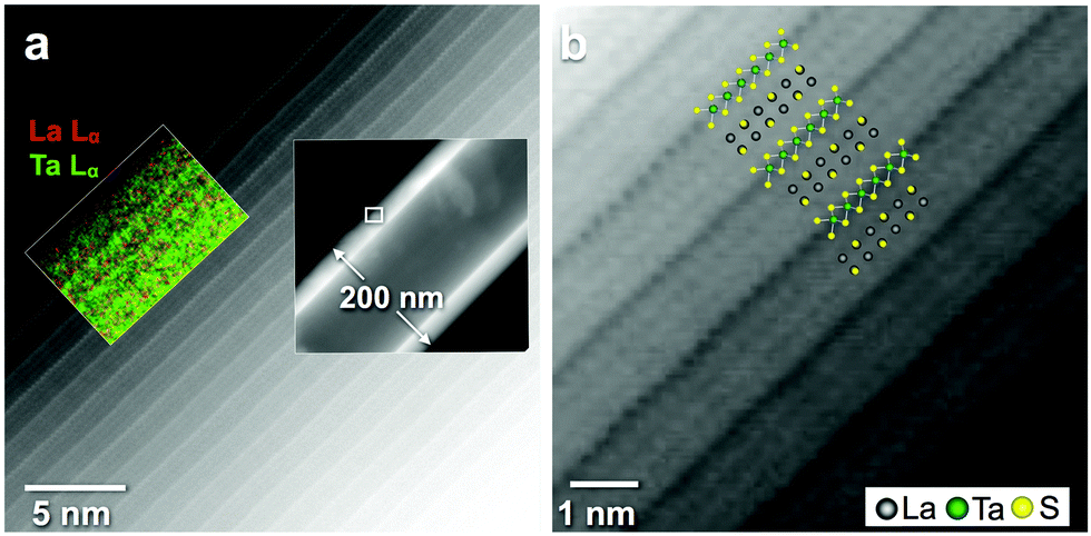 | ||
| Fig. 4 High-resolution STEM images of a LaS–TaS2 nanotube. (a) HAADF image. The insets show an HAADF image corresponding to a larger field of view, with a marker indicating the magnified region, and a high-resolution chemical map acquired by EDS. (b) Atomic-resolution BF STEM image, with structure projections of the LaS and TaS2 layers superimposed. | ||
 | ||
| Fig. 5 Representative XRD pattern recorded from the total product obtained during the synthesis of LaS–TaS2 tubular structures. Different orders of peaks associated with the LnS/TaS2 (1:1) superstructure (SS) along the common c-axis are marked in blue. The corresponding interplanar spacings are also marked. | ||
Stacking disorder of the LnS (with Ln = La, Ce, Nd, Ho, Er) and TaS2 layers along the c-axis was also observed, as shown for a NdS–TaS2 MLC in Fig. S8 in the ESI.† As a result, the basal reflections (marked by a blue bracket in Fig. S8c, ESI†) are smeared. Also, part of the Ta–Ce–S tubules were found to exhibit a periodicity of 2.43 nm along the c-axis, as shown in Fig. S7b in the ESI.† This periodicity is more than twice the regular periodicity of 1.145 nm, which corresponds to the CeS/TaS2 (1:1) periodic stacking. The structure of these Ta–Ce–S nanotubes could not be fully interpreted at this point.
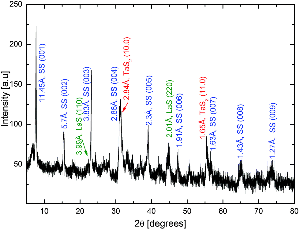
X-ray diffraction (XRD) patterns recorded from the total products obtained during the attempts to synthesize LaS–TaS2, NdS–TaS2 and ErS–TaS2 tubular structures are shown in Fig. 5 and Fig. S4 in the ESI.† A series of different diffraction orders 00n (basal reflections similar to the reflections marked by small blue arrows in the SAED patterns), corresponding to the LnS–TaS2 MLC (superstructures) with LnS and TaS2 layers stacked periodically along the c-axis, can be clearly identified. For the 001 (first order) superstructure peaks, corresponding values of 11.45 Å, 11.28 Å and 11.11 Å were obtained for LaS–TaS2, NdS–TaS2 and ErS–TaS2 MLC, respectively. The line profiles generated from (HRTEM) images yielded quite similar values of 11.5 Å, 11.4 Å and 11.1 Å.
Other XRD peaks were assigned to the non-basal reflections arising from the structurally modulated LnS and TaS2 layers. The (11.0), (10.0) planes of TaS2 (or 200 and 020 respectively according to the ortho-pseudohexagonal system of labeling) as well as (110) and (220) planes of LnS within the LnS–TaS2 MLC are marked on the patterns (the 020 peaks of LnS coincide and 200 roughly coincide with that of 10.0 of TaS2). These diffraction peaks correspond to the SAED peaks marked by the red and green markers respectively in Fig. 3a, b and Fig. S6a in the ESI.†
It is known from the literature1,2,16 that for most of the MLC in their planar form a shift of b/2 along the b-axis between two consequent layers of the same type is observed leading by that to a “doubling” of the periodicity along the stacking direction for that specific subsystem. The stacking is named C-centered when its periodicity is 11–12 Å (with no b/2 shift) and F-centered when the periodicity is twice that distance, i.e. 22–24 Å (i.e. including the b/2 shift). These configurations were actually determined from the intensity-ratio of the TX2 and the MX peaks of the XRD patterns (in some cases with the assistance of SAED patterns of planar sheets).1,16 It is possible that the periodicity of one of the subsystems, e.g. TX2 would be twofold of MX or vice versa. (Four possibilities are possible CC, CF, FC and FF, the first letter corresponds to MX and the second to TX2)1,2,16 However, in the tubular structures described above the situation is even more complex. The successive layers of the same type might also be slightly shifted one with respect to the other due to the folding of each layer into a tube of a slightly different diameter. As stated earlier, many tubes reported here possess a single folding vector of the LnS(Se) and the TaS2(Se) layers with one common b-axis coinciding with the tubule axis. However, a fraction of the analyzed LnS(Se)–TaS2(Se) nanotubes exhibited different rotational variants of the LnS(Se) and the TaS2(Se) layers with two different mutual orientations (between the LnS(Se) and TaS2(Se)) and orientations relative to the tubule axis as detailed in Section S1.1 in the ESI.† This situation is completely analogous to the case of the PbS–TaS27 and PbS–NbS214 nanotubes described before. Therefore the consequent layers of the same type are not only “shifted” but also rotated one relative to the other. Since XRD is obtained from the whole product the ratios of the peak's intensities can not be directly related with the type of centering (the b/2 movement of the consequent layers of the same type related to planar crystals). Also, it was shown previously from SAED data that the b/2 shifts deduced from XRD are not a general feature and often occur non-systematically even for planar crystallites.16
It is well established that, in contrast to planar crystals, the Bragg conditions for diffractions from the basal as well as from non-basal planes can be potentially fulfilled simultaneously within the same tubule (for different incidence θ angles). For a tubule lying on a plane surface (parallel to the sample plane) the basal (XRD) reflections are obtained from the upper and the bottom part of the tubule. However the diffraction from the hk0 planes of LnS and the TaS2 are obtained from the side walls of the tubule. Therefore, in the case of nanotubes, diffraction peaks can be produced from both, for the correct incident angles according to the Bragg's law. Therefore the difference between the intensities of the basal and the non basal reflections cannot be attributed to preferred orientation (texture). XRD patterns representing texture are well documented in the literature for the case of planar (non-tubular) crystallites (see p. 14 in ref. 1).
Peaks arising from the residual by-products, such as pristine LnS (Ln = La, Nd, Er), (and also 1T–TaS2 in Fig. S4a and b, ESI†) and excess unreacted metallic Ln or Ta were also observed however for simplicity reasons they are not marked in the XRD patterns.
The 00n XRD peaks are rather broad (full width at half maximum ∼0.3 Å for the 001 first order reflection). This suggests the presence of a statistical distribution for the interlayer spacing along the c-axis of the LnS/TaS2 (1:1) superstructure. This observation was also confirmed by statistical analysis of electron diffraction data. Furthermore, a spreading of ∼3% in the (10.0) and (11.0) in-plane interplanar spacing for TaS2 and (110) and (220) in-plane interplanar spacing for LnS was observed in the analysis of the SAED patterns recorded from multiple (20–30) tubes. For every compound, average values for the mentioned spacings were calculated and tubules fitting these values were chosen for presentation. The mentioned spreading of 3% refers to the maximum difference between the upper and the lower measured values of the mentioned interplanar spacings for every compound individually.
The values of the interplanar spacing obtained from the SAED/XRD patterns are comparable to published values for the bulk MLC materials (see Table S1, ESI†). No XRD patterns were recorded from CeS–TaS2, HoS–TaS2 or LaSe–TaSe2 due to the low yield of nanotubes in the products. In these compounds, the periodicity was determined solely from SAED patterns, as summarized in Table 2.
All the LnS compounds that are discussed here are stable in bulk form, with NaCl crystal structures and space group Fm![[3 with combining macron]](https://www.rsc.org/images/entities/char_0033_0304.gif) m. However, as a result of the mutual structural modulation that occurs in MLC, the structures of bilayers are distorted slightly when compared to the pristine bulk phase. The interplanar spacings of TaS2 and LnS (with Ln = La, Ce, Nd, Er) within bulk LnS–TaS2 MLC, as well as their values in pristine bulk form, are given in Table S1 in the ESI.† To the best of our knowledge, bulk HoS–TaS2 and LaSe–TaSe2 MLC have not been reported previously. Therefore, in these cases only values for bulk HoS, LaSe, TaS2 and TaSe2 are given in this table.
m. However, as a result of the mutual structural modulation that occurs in MLC, the structures of bilayers are distorted slightly when compared to the pristine bulk phase. The interplanar spacings of TaS2 and LnS (with Ln = La, Ce, Nd, Er) within bulk LnS–TaS2 MLC, as well as their values in pristine bulk form, are given in Table S1 in the ESI.† To the best of our knowledge, bulk HoS–TaS2 and LaSe–TaSe2 MLC have not been reported previously. Therefore, in these cases only values for bulk HoS, LaSe, TaS2 and TaSe2 are given in this table.
The in-plane and c-axis lattice constants of tubular structures of the LnS–TaS2 MLC are smaller than those of their MS–TaS2 (M = Sn, Pb) counterparts. Since the Ln atoms prefer a trivalent state, while Pb and Sn are divalent, charge transfer from the LnS layers to the TaS2 layers is expected to be greater than for PbS or SnS.7,8,10 BiS–TaS2 and SbS–TaS2 can be considered as an intermediate case.1,7,8,17,18 Most of the Sb and Bi atoms in SbS and BiS are believed to be trivalent just as in their well known bulk compounds Sb2S3 and Bi2S3 respectively.19 Strong charge transfer may result in a stronger electrostatic interaction between the LnS and TaS2 layers, and consequently shorter bond lengths between the Ln and S atoms of the TaS2 layer,8i.e., smaller periodicity values along the c-axis (see Fig. 6).
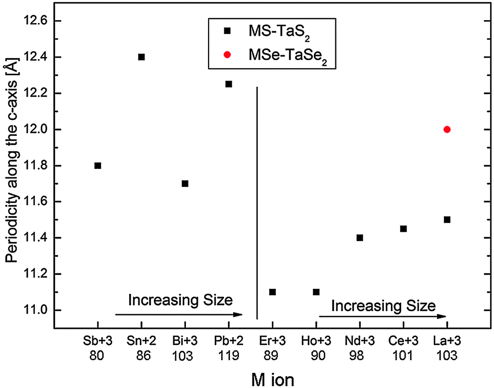 | ||
| Fig. 6 Values of c-axis periodicity for tubular structures of MX–TX2 MLC, presented schematically for the series of M atoms with increasing ionic radius shown in ascending order. The ionic radii of the M atoms in picometers are taken from Shannon–Prewitt Effective Ionic Radius at http://www.knowledgedoor.com/2/elements_handbook/shannon-prewitt_effective_ionic_radius.html and references thereof. Values for the MLC nanotubes with M = Sn, Pb, Sb and Bi are reproduced from data published previously7,18 for comparison. | ||
Presumably, charge transfer between the two sublattices is responsible for the abundance of LnS–TaS2 tubules that have a single folding vector in these samples. Despite the crystallographic equivalence of the 60° rotation of the LnS relative to the TaS2 layer (see Fig. S1 in the ESI†), their orientations relative to the tubule axis are different. Obviously, only one (out of the three equivalent) common b axes between the LnS and TaS2 of the LnS–TaS2 slab can coincide with the nanotube axis (see Fig. S1 in the ESI†). Therefore, the b-axis of only one LnS layer (out of three) will coincide with the tubule axis. The energy associated with folding is believed to be minimal for the LnS layer, whose b-axis coincides with the tubule axis. Since the coupling between the layers is strong, it is believed that LnS–TaS2 slabs without these rotational variants can be transformed more easily into nanotubes. This situation is obviously not the case for, e.g., MS–TS2 (M = Pb; T = Nb, Ta) tubules, in which the interlayer interaction is not as strong and tubules with three folding vectors for the MS layers and two folding vectors for the TS2 layers are produced.7,14
Table 2 and Fig. 6 show that both the average interplanar periodicity along the c-axis corresponding to the LnS–TaS2 (1:1) superstructure and the in-plane interplanar spacings decrease with increasing atomic number of Ln (i.e., La, Ce, Nd, Ho, Er). Similar behavior was observed for bulk single crystals of LnS–TaS2 MLC10 and for tubular structures of MLC that are based on LnS–CrS2.20 This trend can be attributed to a decrease in the size of the Ln+3 ion with increasing atomic number. Similarly, the greater values of c-axis periodicity in LaSe–TaSe2, when compared to that in isostructural LaS–TaS2, can be attributed to the larger ionic radius of Se and the more covalent nature of its bonding with the metal atoms. For the sake of comparison, the interlayer spacing of nanotubes of the MS–TaS2 compounds with M = Sb, Sn, Bi and Pb are shown on the left side of the graph. Noticeably, the interlayer spacing of the MLC with stable Sn2+ and Pb2+ is larger than that of the MLC with Sb+3 and Bi+3 and the trivalent lanthanides. This observation suggests that the stability of the stable MLC with M+3 is attained by a significant degree of charge transfer from the metal M to the Ta atom.
Electronic structure
The density-functional tight-binding (DFTB)21,22 method was used to calculate the electronic structure of bulk LaS–TaS2 as shown in Fig. 7. (The electronic structures obtained by the DFTB method are comparable to the full density functional theory (DFT) method as shown in Fig. S9 (ESI†). Therefore the use of the DFTB method for the calculations is justified.) The electronic structure including local densities of states, atom-resolved charges and the resulting charge transfer of this specific family of MLC were not reported before. Since the lattice structure is incommensurate along the a-direction (aLaS/aTaS2 is an irrational number), a supercell approximation which is identical to that of previous publications,23i.e. 4 × aLaS ≈ 7 × aTaS2 was used. This cell (see Fig. 7a) contains four sublayers (2 LaS and 2 TaS2) due to the fact, that this compound forms a so called CF structure (see Fig. 4 in ref. S7) with an inversion center between the two TaS2 sublayers.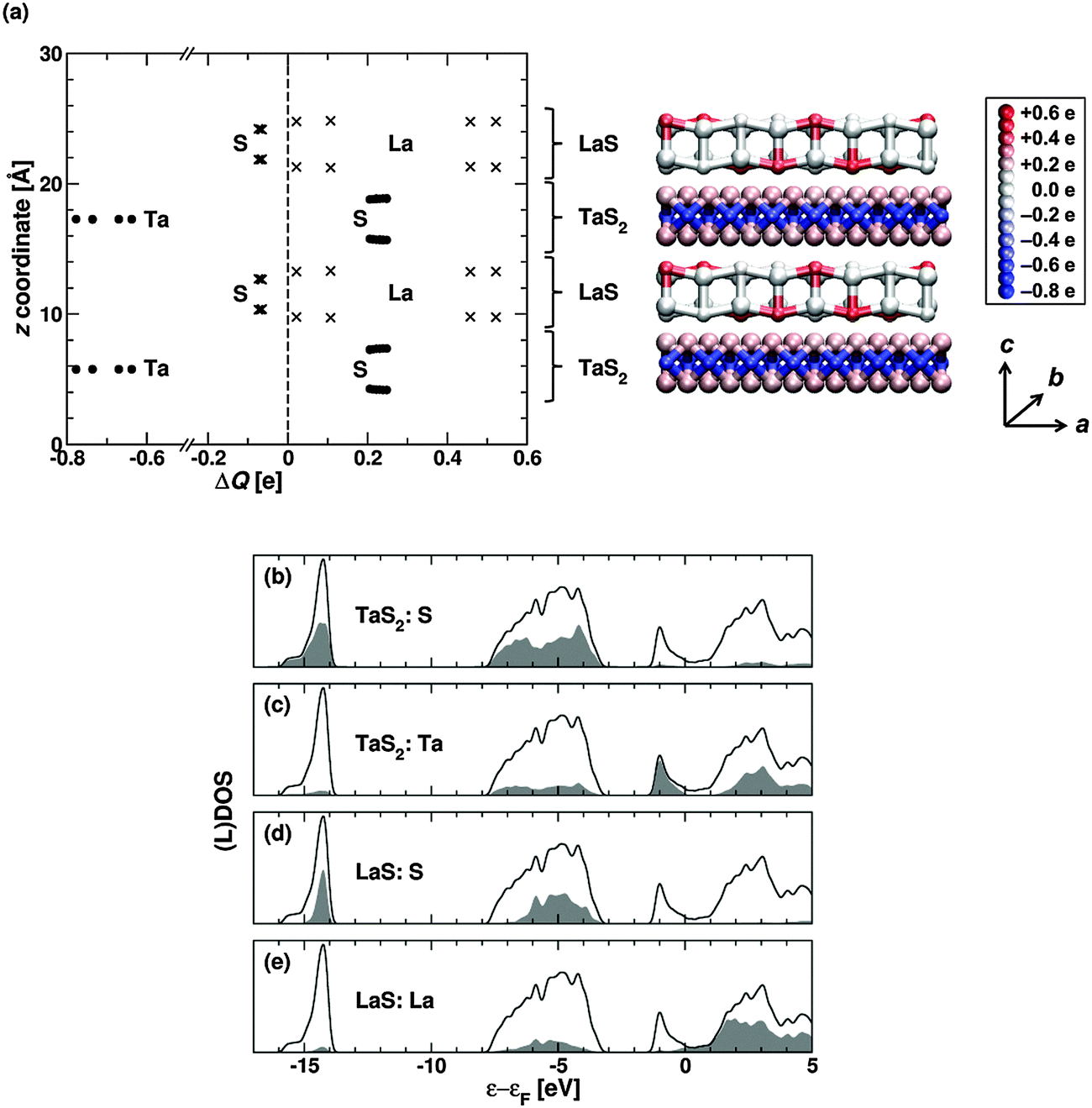 | ||
| Fig. 7 (a) The changes in the atomic charges (ΔQ) of the atoms in the compound, compared to the charges of the atoms of the isolated LaS and TaS2 layers. The structure is shown in a view along the normal to the (020) plane of a LaS–TaS2 unit cell (labeled according to the ortho-pseudohexagonal system for TaS2). The individual atoms are colored according to the ΔQ values in the left diagram with a color code shown on the right side. The “−” and “+” signs represent gained and donated (depleted) electronic charges, respectively. The La atoms (small spheres) are shown in different hues of gray to pink, depending on their positions relative to the TaS2 sublayer and subsequent ΔQ. The Ta atoms (small spheres) are colored in blue and the S (large spheres) atoms in pink in the TaS2 sublayer and in grey in the LaS sublayer. (b–e) Show the total and local density of states for the LaS–TaS2 compound. The solid black lines correspond to total DOS curves. The local densities of states of the atom types are shown in grey: (b) S atoms and (c) Ta atoms in the TaS2 sublayer, (d) S atoms and (e) La atoms in the LaS sublattice. The energy is given relative to the Fermi energy of the LaS–TaS2 compound. | ||
From the isolated LaS and TaS2 sublayers, one would expect electron transfer from La to Ta in the combined system (see the DOS curves of LaS and TaS2 in Fig. S10 in the ESI†). The calculated DOS of the LaS–TaS2 compound is shown in Fig. 7b–e (solid black curve). An analysis of the integrated local density of states (LDOS) as well as a Mulliken population analysis show an increase of the electron density on the Ta atoms and a decrease of the electron density on the La atoms in the LaS–TaS2 system compared to the isolated LaS/TaS2 layers. Different values of the transferred charges ΔQ (relative to their charges in the pristine LaS and TaS2 layers) were obtained for the different La atoms (see Fig. 7a). This results from the different lattices of the subsystems and consequently from different positions of the La atoms relative to the atoms in the TaS2 sublayers. The variation in charge transfer to the Ta atoms in the unit cell is much smaller (see Fig. 7a) due to the shielding of the Ta atoms by the sulfur atoms. The smallest spreading of the charge transfer was found for the sulfur atoms within the two sublayers. On average every La atom has lost 0.28 electrons, while every Ta atom has gained 0.69 electrons, compared to the isolated monolayers (see Fig. 7a and Table S2 in the ESI†). I.e. the electron transfer from the La d-states to the Ta d-states is compensated to some extent by corresponding changes in the S charges in each subsystem (see Table S2, ESI†) which is opposed in sign relative to the metal atoms.
Consequently, a relatively small net electron transfer between the TaS2 and LaS layers (∼0.2 electrons per formula unit) occurs. The charge transfer from the La to the Ta atom is dominated by the states near the Fermi level and results in a filled dz2 band of the Ta atoms in the combined system (Fig. 7c). Whereas both isolated monolayers have pronounced metallic character (Fig. S10, ESI†), the LaS–TaS2 compound has an overall semimetallic behavior, in which the TaS2 layers are almost semimetallic and the LaS layers are effectively nonmetallic. A more detailed discussion of the electronic structure will be given in a separate publication.
Raman spectroscopy
Raman spectroscopy measurements were carried-out on single LaS–TaS2 and NdS–TaS2 tubular crystals of 200–500 nm thickness (see Fig. 8). The differences between the Raman modes of pristine bulk LnS24 and 2H–TaS225 and the modes observed in the corresponding MLC can be interpreted in terms of charge transfer from the LnS to the TaS2 layers.25 Charge transfer increases both the intralayer and the interlayer interaction between the layers, thereby affecting the Raman frequencies. In addition, the Raman spectra are expected to be affected by the mutual structural modulation. Recall that the structure of the LnS layers (and to a lesser extent that of the TaS2 layers) within the MLC is slightly different from bulk LnS with a NaCl structure.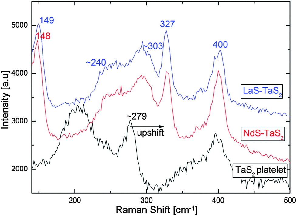 | ||
| Fig. 8 Raman spectra of single LaS–TaS2 and NdS–TaS2 tubular crystals. A spectrum recorded from a TaS2 platelet is also shown for comparison. | ||
Representative Raman spectra recorded from single tubular nanocrystals of LaS–TaS2 and NdS–TaS2 are shown in Fig. 8. A spectrum of a 2H–TaS2 platelet was measured for comparison as well. The spectra recorded from LaS–TaS2 MLC tubular crystals are in excellent agreement with the results published previously for a bulk single crystal of LaS–TaS2 MLC.25
The mode at 400 cm−1 is in perfect agreement with the A1g (intralayer out-of-plane vibration) mode of 2H–TaS2.25 The mode at 327 cm−1 is attributed to the E2g (intralayer in-plane vibration) mode, which occurs at 286 cm−1 in bulk 2H–TaS2.25 The large upshift of the intralayer E2g mode of the TaS2 (41 cm−1 in this case) has been reported for various intercalation compounds of 2H–TaS2 (and 2H–NbS2), including the misfit compounds25–27 and is attributed to charge transfer from the LnS to the TaS2 layers. The mode at ∼149 cm−1 matches the A1g (intralayer out-of-plane vibration) mode at 148 cm−1 of LaS in a LaS–TaS2 MLC single crystal. An additional A1g mode at 122 cm−1 was observed by Kisoda et al.25 but was not observed here due to experimental limitations at lower wavenumbers. As mentioned previously, the observed Raman modes of the LaS layers within LaS–TaS2 MLC are different from the modes observed in LaS bulk single crystals with NaCl structure.24 The broad band between ∼240 and 303 cm−1 is attributed to the two-phonon band as detailed elsewhere.25
The spectra recorded from NdS–TaS2 tubular crystals are quite similar to their LaS–TaS2 counterparts. However, no previous literature data could be found for bulk NdS–TaS2 MLC. Inasmuch as spectra recorded from bulk LnS–TaS2 MLC with (Ln = La, Ce, Sm and Gd) were found to be similar,25 the similarity of NdS–TaS2 is not surprising.
Conclusions
Nanotubular structures were formed from LnS–TaS2 (Ln = La, Ce, Nd, Ho, Er) and LaSe–TaSe2 MLC in evacuated silica tubes when subjected to appropriate temperature profiles and growth times. The compounds were found to be commensurate along the b-axis and incommensurate along the a-axis. SAED patterns of the tubes suggest a single folding vector for the LnS(Se) and TaS2(Se) layers in many cases. As expected, the commensurate b-axes of the LnS(Se) and TaS2(Se) layers coincide with the tubule axis.The mutual structural modulation of the TaS2(Se) and LnS(Se) lattices results in an orthorhombic distortion of the rocksalt LnS(Se) lattice, while the TaS2(Se) is barely modified. The difference between the in-plane lattice parameters (a and b) of LnS in LnS–TaS2 MLC became more significant for HoS and ErS than for LaS, LaSe, CeS and NdS. Both the c-axis periodicity of the LnS–TaS2 superstructure and the in-plane lattice periodicities of the LnS and TaS2 layers decrease with increasing atomic number of Ln. The periodicity is greater for selenides than for corresponding sulfides.
The smaller periodicities in the LnS–TaS2 tubules relative to their SnS–TaS2 and PbS–TaS2 counterparts indicate a stronger interaction between the two subsystems for the former. Such an observation is supported by a high upshift in the E2g Raman mode of TaS2 in these compounds. Theoretical calculations for LaS–TaS2 indicate a small net charge transfer from the LaS layer to the hexagonal sublattice. But on the other hand, also larger changes of the metal atom's charges and consequently of the occupations of their electronic states can be observed. This results in a nearly full occupied dz2 band in the TaS2 subsystem. Hence, the electronic structure of the TaS2 part is comparable to that of MoS2 or WS2.
Competing financial interest
The authors declare no competing financial interest.Acknowledgements
RT acknowledges the support of the Israel Science Foundation; German-Israeli Foundation (GIF); The FTA action of the Israel National Nano-Initiative; the H. Perlman Foundation; the G. M. J. Schmidt Minerva Center for Supramolecular Chemistry; the Irving and Azelle Waltcher Foundations in honor of Prof. M. Levy and the Irving and Cherna Moskowitz Center for Nano and Bio-Nano Imaging. GS, JOJ and TL would like to acknowledge the financial support of the DFG (ICENAP project), for computational time provided by ZIH Dresden (project QDSIM) and for helpful discussions with I. Baburin, K. Trepte and D. Lenz.References
- G. A. Wiegers, Prog. Solid State Chem., 1996, 24, 1–139 CrossRef CAS.
- G. A. Wiegers and A. J. Meerschaut, J. Alloys Compd., 1992, 178, 351–368 CrossRef CAS.
- F. Jellinek, J. Less-Common Met., 1962, 4, 9–16 CrossRef.
- A. H. Thompson, R. F. Gamble and J. F. Revelli, Solid State Commun., 1971, 9, 981–985 CrossRef CAS.
- J. F. Revelli, Inorg. Synth., 1979, 19, 35–49 CrossRef CAS.
- A. Meetsma, G. A. Wiegers, R. J. Haange and J. L. de Boer, Acta Crystallogr., Sect. C: Cryst. Struct. Commun., 1990, 46, 1598–1599 CrossRef.
- G. Radovsky, R. Popovitz-Biro and R. Tenne, Chem. Mater., 2014, 26, 3757–3770 CrossRef CAS.
- G. A. Wiegers, J. Alloys Compd., 1995, 219, 152–156 CrossRef CAS.
- F. J. Di-Salvo, G. W. Hull, L. H. Schwartz, J. M. Voorhoeve and J. V. Waszczak, J. Chem. Phys., 1973, 59, 1922–1929 CrossRef CAS.
- K. Suzuki, T. Enoki and K. Imaeda, Solid State Commun., 1991, 78, 73–77 CrossRef CAS.
- D. Reefman, J. Baak, H. B. Brom and G. A. Wiegers, Solid State Commun., 1990, 75, 47–51 CrossRef CAS.
- N. Katayama, M. Nohara and H. Tagaki, Phys. C, 2006, 445, 35–38 CrossRef.
- D. Bernaerts, S. Amelinckx, G. van Tendeloo and J. van Landuyt, J. Cryst. Growth, 1997, 172, 433–439 CrossRef CAS.
- G. Radovsky, R. Popovitz-Biro, D. G. Stroppa, L. Houben and R. Tenne, Acc. Chem. Res., 2014, 47, 406–416 CrossRef CAS PubMed.
- J. L. de Boer, A. Meetsma, T. J. Zeinstra, R. J. Haange and G. A. Wiegers, Acta Crystallogr., Sect. C: Cryst. Struct. Commun., 1991, C47, 924–930 CrossRef CAS.
- S. Kuypers, J. van Landuyt and S. Amelinckx, J. Solid State Chem., 1990, 86, 212–232 CrossRef CAS.
- G. A. Wiegers, Jpn. J. Appl. Phys., 1993, 32, 705–710 CrossRef CAS.
- L. S. Panchakarla, G. Radovsky, L. Houben, R. Popovitz-Biro, R. E. Dunin-Borkowski and R. Tenne, J. Phys. Chem. Lett., 2014, 5, 3724–3736 CrossRef CAS PubMed.
- Y. Ren, C. Haas and G. A. Wiegers, J. Phys.: Condens. Matter, 1995, 7, 5949–5958 CrossRef.
- L. S. Panchakarla, R. Popovitz-Biro, L. Houben, R. E. Dunin-Borkowski and R. Tenne, Angew. Chem., Int. Ed., 2014, 53, 6920–6924 CrossRef CAS PubMed.
- D. Porezag, T. Frauenheim, T. Köhler, G. Seifert and R. Kaschner, Phys. Rev. B: Condens. Matter Mater. Phys., 1995, 51, 12947–12957 CrossRef CAS.
- G. Seifert, D. Porezag and T. Frauenheim, Int. J. Quantum Chem., 1996, 58, 185–192 CrossRef CAS.
- C. M. Fang, S. van Smaalen, G. A. Wiegers, C. Haas and R. A. de Groot, J. Phys.: Condens. Matter, 1996, 8, 5367–5382 CrossRef CAS.
- I. Morke, E. Kaldis and P. Wachter, Phys. Rev. B: Condens. Matter Mater. Phys., 1986, 33, 3392–3398 CrossRef.
- K. Kisoda, M. Hangyo, S. Nakashima, K. Suzuki, T. Enoki and Y. Ohno, J. Phys.: Condens. Matter, 1995, 7, 5383–5393 CrossRef CAS.
- M. Hangyo, K. Kisoda, S. Nakashima, A. Meerschaut and J. Rouxel, Phys. B, 1996, 219–220, 481–483 CrossRef.
- M. Hangyo, K. Kisoda, T. Nishio, S. Nakashima, T. Terashima and N. Kojima, Phys. Rev. B: Condens. Matter Mater. Phys., 1994, 50, 12033–12043 CrossRef CAS.
Footnote |
| † Electronic supplementary information (ESI) available: Structural aspects of the nanotubes, chemical analysis of the products, SEM images of the products, X-ray diffraction analysis of the product, tubular structures from LnS–TaS2 (Ln = Ce, Nd, Ho) and LaSe–TaSe2 MLC, literature values of interplanar spacings of TaS2(Se) and LnS(Se), theoretical calculations. See DOI: 10.1039/c5tc02983j |
| This journal is © The Royal Society of Chemistry 2016 |