A room-temperature environmentally friendly solution process to assemble silver nanowire architectures for flexible transparent electrodes†
Ye
Yang‡
,
Jin-Long
Wang‡
,
Lei
Liu
,
Zhi-Hua
Wang
,
Jian-Wei
Liu
* and
Shu-Hong
Yu
 *
*
Division of Nanomaterials & Chemistry, Hefei National Laboratory for Physical Sciences at the Microscale, Collaborative Innovation Center of Suzhou Nano Science and Technology, Department of Chemistry, CAS Center for Excellence in Nanoscience, Hefei Science Center of CAS, University of Science and Technology of China, Hefei 230026, China. E-mail: jwliu13@ustc.edu.cn; shyu@ustc.edu.cn; Fax: +86 0551 63603040
First published on 4th November 2016
Abstract
In this study, we present a room-temperature environmentally friendly solution process to optimize the performance of the flexible transparent electrodes by co-assembling Ag nanowires and CaCO3 nanowires, and then etching CaCO3 nanowires away, leaving Ag nanowire networks with controllable optical transparency and electrical conductivity. The obtained Ag nanowire flexible transparent electrodes exhibit an averaged transmittance of up to 90% when the sheet resistance is 70 Ω sq−1 which shows no degradation even after 2000 cycles of fatigue test, indicating their excellent mechanical flexibility and stability.
In recent years, flexible transparent electrodes have attracted much attention in the fabrication of modern devices, such as optoelectronic devices, organic light-emitting diodes (OLEDs), solar cells, photodetectors, etc.1–4 Optical transparency and electrical conductivity are both important parameters in the various applications of transparent conductive films. Traditionally, indium tin oxide (ITO) electrodes, which are transparent and colorless, have been widely used in transparent conducting optoelectronic devices.5–7 However, there are still some disadvantages of ITO electrodes, such as the rarity of indium, the high cost of manufacturing technology, and their mechanical brittleness. It is reported that ITO replacement is a large and fast growing market, and it is predicted to reach 8.1 billion US dollars by 2021. So far, to replace ITO, researchers have used metal nanowires, graphene, carbon nanotubes (CNTs) and conductive polymers to fabricate highly transparent flexible electrodes with low resistance.4,8–10 Among them, thin films of Ag nanowires show very promising results as alternatives to the indium tin oxide based electrodes because of their high conductivity and optical transmittance.11 Because the random metal nanowire networks always make it difficult to balance the optical and conductive properties, macroscopic-scale well-defined nanowire architectures with tailorable performances is one of the good choices for fabrication of flexible transparent electrodes.12 Recently, a variety of principles and strategies have been introduced to assemble nanowires, including interface induced nanowire assembly,13,14 shear force induced assembly,15,16 nanowire orientation by extra fields17 and electrospinning processes.18 As an attractive assembly strategy, the Langmuir–Blodgett (LB) technique has been explored to assemble both stiff nanowires (Ag, PbS, Ge nanowires, etc.)16,19,20 and flexible nanowires (Te nanowires and W18O49 nanowires, etc.).14,21
Recently, our group reported a LB strategy to manipulate nanowire assemblies for flexible transparent electrodes.22 During the fabrication process, Te nanowires were used as a spacer to tune the pitch of the Ag nanowire networks to optimize the optical transmittance and the conductivity, while its high cost, toxicity and the rarity of reserves limit the wide applications of these electrodes. To replace Te nanowires and optimize the electrode fabrication process, an environmentally friendly, low-cost, and facile method should be introduced to accelerate the market applications. Calcium carbonate is a common nontoxic mineral and is the main component of pearls and the shells of marine organisms, snails, and eggs which can be easily obtained on a large scale.23–26
Herein, we report a room-temperature solution process for fabrication of silver nanowire based flexible transparent electrodes. Firstly, Ag nanowires and CaCO3 nanowires with different mole ratios are co-assembled into ordered nanowire structures using the LB technique. Then the CaCO3 nanowires are etched away, leaving Ag nanowire networks with a tunable nanowire separation distance. Throughout the construction process, CaCO3 remains nontoxic and its synthesis from mussel shells is an environmentally friendly method. Moreover, the products after etching process are water and carbon dioxide which cause no pollution to the environment. After embedding the Ag nanowire networks in PVA (polyvinyl alcohol) films, we obtain the flexible transparent conducting electrode with the best optical transmittance of 90% when the square resistance is 70 Ω sq−1.
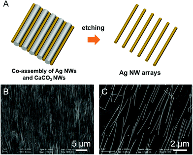
Fig. 1A illustrates the nanowire assembly process to manipulate Ag nanowires and tailor their spacing. Briefly, aragonite CaCO3 nanowires with a length of 20 μm and a diameter of 100 nm were obtained by dissolving the connecting part of the mussel shells in the solution of sodium hypochlorite (Experimental section in the ESI, and Fig. S1A, ESI†). The raw materials are low-cost which can be easily found in the market. The phase of the obtained nanowires was confirmed by the X-ray diffraction (XRD) pattern shown in Fig. S1B.† All peaks in this spectrum can be easily indexed to the aragonite phase of calcium carbonate, which are in good agreement with the standard JCPDF card data (JCPDF card number: 41-1475). In the meantime, Ag nanowires with a length of 5 μm and a diameter of 50 nm were synthesized according to the previous report.27 Their morphology and phase are shown in Fig. S2A and S2B.† After mixing the two kinds of nanowires and assembling them into an ordered nanowire array by the LB technique (Fig. 1B),28 the obtained nanowire film was then immersed in a dilute acetic acid solution (10%, v/v%) for 30 min to remove the CaCO3 nanowires away, resulting in an Ag nanowire monolayer on the substrate(Fig. 1C). From the following chemical equation, it was found that the products are water and carbon dioxide which cause no pollution to the environment.
| 2CH3COOH + CaCO3 → (CH3COO)2Ca + CO2↑ + H2O |
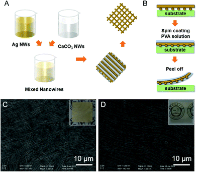
The space between the Ag nanowires could be tuned by changing the molar ratio of the two mixed nanowires. CaCO3 nanowires used here as a spacer have several advantages: (1) CaCO3 nanowires used here are morphologically uniform (diameter and aspect ratio) and have a highly pure phase; (2) the fabrication of harmless CaCO3 nanowires is simple and low-cost due to the abundance of raw materials; (3) after reacting with the acid solution, no residue would be left on the substrate. Fabrication of complex nanowire networks with high conductivity is necessary to meet the demands of high-quality flexible transparent conductive electrodes which is illustrated in Fig. 2A and B. Double layered Ag–CaCO3 nanowire films were constructed by the LB technique reported previously.14 Because of their closed-packing (Fig. 2C), the nanowire films are opaque which is shown in the inset of Fig. 2C. As discussed above, transparent and conductive Ag nanowire networks with mesh-like crossed patterns can be constructed after the CaCO3 nanowires are removed (Fig. 2D and its inset). To fabricate flexible electrodes with high stability in air, we transferred Ag nanowire networks from the polycarbonate (PC) substrate to PVA substrates. That is, after the removal of CaCO3 nanowires, a PVA solution (10 wt%) is spin-coated over the Ag nanowire networks and then the PVA matrix is peeled off after drying as illustrated in Fig. 2B.
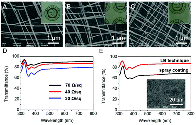
Excellent conductivity and transmittance are crucial for the wide applications of flexible transparent electrodes.1,29 By tuning the molar ratio of the two assembled nanowires to control the pitch of Ag nanowire networks, we can tailor and balance the conductivity and transmittance to fully improve their performance. With different molar ratios of CaCO3 nanowires and Ag nanowires, the pore area of the Ag nanowire networks could be significantly different. Fig. 3A–D show the SEM images and conductivity of nanowire films to illustrate the relationship between the density of nanowire networks and the properties of the films. As shown in Fig. 3A–C, the pore area decreases with the increasing content of Ag nanowires (molar ratios: 1![[thin space (1/6-em)]](https://www.rsc.org/images/entities/char_2009.gif) :
:![[thin space (1/6-em)]](https://www.rsc.org/images/entities/char_2009.gif) 2.5, 1
2.5, 1![[thin space (1/6-em)]](https://www.rsc.org/images/entities/char_2009.gif) :
:![[thin space (1/6-em)]](https://www.rsc.org/images/entities/char_2009.gif) 5, and 1
5, and 1![[thin space (1/6-em)]](https://www.rsc.org/images/entities/char_2009.gif) :
:![[thin space (1/6-em)]](https://www.rsc.org/images/entities/char_2009.gif) 10). The corresponding transmittance changes from 90%, 85% to 75%, while the conductivity is tuned from 70, 40 to 30 Ω sq−1 (Fig. 3D). It was found that lower densities of AgNWs resulted in a higher transmittance and a higher sheet resistance. Compared with the random Ag nanowire films prepared by spray coating, the transmittance of well-arranged Ag nanowire electrodes obtained by the LB technique is much higher with the same conductivity (Fig. 3E).30
10). The corresponding transmittance changes from 90%, 85% to 75%, while the conductivity is tuned from 70, 40 to 30 Ω sq−1 (Fig. 3D). It was found that lower densities of AgNWs resulted in a higher transmittance and a higher sheet resistance. Compared with the random Ag nanowire films prepared by spray coating, the transmittance of well-arranged Ag nanowire electrodes obtained by the LB technique is much higher with the same conductivity (Fig. 3E).30
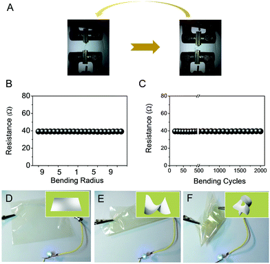
Besides the conductivity and transmittance, compared with ITO, a major advantage of metal nanowire films is their mechanical flexibility.31–33Fig. 4A illustrates a fatigue test of Ag nanowire film with a transmittance of 85% from a flat state to a radius of curvature of 2.0 mm to demonstrate their mechanical properties and flexibility. The electrical performance of response to the bending test was carried out with a high-precision mechanical system (Instron 5565A) and a Keithley 4200 SCS in a clean and metal-shielded box which is shown in Fig. 4B and C. During the first bending cycle, the resistance of the nanowire film remained constant even at a bending radius of 2.0 mm, as shown in Fig. 4B. In the experiment to test the stability and robustness of our Ag nanowire flexible networks, the conductive resistance hardly changed even after more than 2000 bending cycles (changing from 40 Ω to 39.2 Ω) (Fig. 4C). As shown in Fig. S3,† the PVA matrix protected Ag nanowire networks from destruction, mesh-like crossed patterns can still be observed after the fatigue test. Furthermore, these electrodes retained their conductivity consistently even when the device was twisted and bent into any shape (Fig. 4D–F), indicating the full flexibility of the electrode.
Conclusions
In summary, we report a room-temperature environmentally friendly solution process to construct Ag nanowire flexible transparent electrodes. During the fabrication process, CaCO3 nanowires can be used as a spacer to tune the pitch of the Ag nanowire networks to optimize the optical transmittance and electrical conductivity. Firstly, CaCO3 nanowires are obtained from natural shells which are low-cost and easy to produce by mass production. Secondly, the product of the etching process are water and carbon dioxide which cause no pollution to the environment. Thirdly, throughout the fabrication process, all the steps are carried out at room temperature in air. The obtained electrodes are fully flexible, transparent and stable, showing the best transmittance of up to 90% when the sheet resistance is 70 Ω sq−1. Moreover, the Ag nanowire electrodes are very stable, and the resistance remains consistent over 2000 cycles of mechanical deformation. Therefore, this work provides the possibility for the fabrication of flexible transparent nanowire network electrodes with optimized optical and electrical properties.Acknowledgements
We acknowledge the funding support from the National Natural Science Foundation of China (Grant 21431006), the Foundation for Innovative Research Groups of the National Natural Science Foundation of China (Grant 21521001), the Key Research Program of Frontier Sciences, CAS (Grant QYZDJ-SSW-SLH036), and the National Basic Research Program of China (Grants 2014CB931800, 2013CB933900). J. W. L. acknowledges the National Natural Science Foundation of China (Grants 51471157 and 21401183), the Youth Innovation Promotion Association of CAS (2014298), the Anhui Provincial Natural Science Foundation (1508085QB28) and the Fundamental Research Funds for the Central Universities (WK2060190026).Notes and references
- K. Ellmer, Nat. Photonics, 2012, 6, 809–817 CrossRef CAS.
- S. Pang, Y. Hernandez, X. Feng and K. Mullen, Adv. Mater., 2011, 23, 2779–2795 CrossRef CAS PubMed.
- Q. Cao and J. A. Rogers, Adv. Mater., 2009, 21, 29–53 CrossRef CAS.
- D. S. Hecht, L. Hu and G. Irvin, Adv. Mater., 2011, 23, 1482–1513 CrossRef CAS PubMed.
- D. A. Rider, R. T. Tucker, B. J. Worfolk, K. M. Krause, A. Lalany, M. J. Brett, J. M. Buriak and K. D. Harris, Nanotechnology, 2011, 22, 085706 CrossRef PubMed.
- Z. A. Tan, W. Zhang, Z. Zhang, D. Qian, Y. Huang, J. Hou and Y. Li, Adv. Mater., 2012, 24, 1476–1481 CrossRef CAS PubMed.
- H. Lu, W. Tian, F. Cao, Y. Ma, B. Gu and L. Li, Adv. Funct. Mater., 2016, 26, 1296–1302 CrossRef CAS.
- A. Kumar and C. Zhou, ACS Nano, 2010, 4, 11–14 CrossRef CAS PubMed.
- S. Bae, H. Kim, Y. Lee, X. Xu, J.-S. Park, Y. Zheng, J. Balakrishnan, T. Lei, H. R. Kim, Y. I. Song, Y.-J. Kim, K. S. Kim, B. Ozyilmaz, J.-H. Ahn, B. H. Hong and S. Iijima, Nat. Nanotechnol., 2010, 5, 574–578 CrossRef CAS PubMed.
- Y. H. Kim, C. Sachse, M. L. Machala, C. May, L. Mueller-Meskamp and K. Leo, Adv. Funct. Mater., 2011, 21, 1076–1081 CrossRef CAS.
- S. Ye, A. R. Rathmell, Z. Chen, I. E. Stewart and B. J. Wiley, Adv. Mater., 2014, 26, 6670–6687 CrossRef CAS PubMed.
- J.-W. Liu, H.-W. Liang and S.-H. Yu, Chem. Rev., 2012, 112, 4770–4799 CrossRef CAS PubMed.
- A. R. Tao, J. X. Huang and P. D. Yang, Acc. Chem. Res., 2008, 41, 1662–1673 CrossRef CAS PubMed.
- J. W. Liu, J. H. Zhu, C. L. Zhang, H. W. Liang and S. H. Yu, J. Am. Chem. Soc., 2010, 132, 8945–8952 CrossRef CAS PubMed.
- J. Yao, H. Yan and C. M. Lieber, Nat. Nanotechnol., 2013, 8, 329–335 CrossRef CAS PubMed.
- J.-W. Liu, J.-L. Wang, W.-R. Huang, L. Yu, X.-F. Ren, W.-C. Wen and S.-H. Yu, Sci. Rep., 2012, 2, 987 CrossRef PubMed.
- M. Mertl, Science, 1999, 283, 775–775 CrossRef CAS PubMed.
- D. Li and Y. N. Xia, Adv. Mater., 2004, 16, 1151–1170 CrossRef CAS.
- I. Patla, S. Acharya, L. Zeiri, J. Israelachvili, S. Efrima and Y. Golan, Nano Lett., 2007, 7, 1459–1462 CrossRef CAS PubMed.
- D. W. Wang, Y. L. Chang, Z. Liu and H. J. Dai, J. Am. Chem. Soc., 2005, 127, 11871–11875 CrossRef CAS PubMed.
- J. W. Liu, J. Zheng, J. L. Wang, J. Xu, H. H. Li and S. H. Yu, Nano Lett., 2013, 13, 3589–3593 CrossRef PubMed.
- J.-W. Liu, J.-L. Wang, Z.-H. Wang, W.-R. Huang and S.-H. Yu, Angew. Chem., Int. Ed., 2014, 53, 13477–13482 CrossRef CAS PubMed.
- A. Arakaki, K. Shimizu, M. Oda, T. Sakamoto, T. Nishimura and T. Kato, Org. Biomol. Chem., 2015, 13, 974–989 Search PubMed.
- C. Li and L. Qi, Angew. Chem., Int. Ed., 2008, 47, 2388–2393 CrossRef CAS PubMed.
- H. Cölfen and S. Mann, Angew. Chem., Int. Ed., 2003, 42, 2350–2365 CrossRef PubMed.
- L. Liu, J. Jiang and S.-H. Yu, Cryst. Growth Des., 2014, 14, 6048–6056 Search PubMed.
- C. Yang, H. Gu, W. Lin, M. M. Yuen, C. P. Wong, M. Xiong and B. Gao, Adv. Mater., 2011, 23, 3052–3056 CrossRef CAS PubMed.
- J.-W. Liu and S.-H. Yu, Natl. Sci. Rev., 2015, 2, 392–393 CrossRef.
- B. Li, S. Ye, I. E. Stewart, S. Alvarez and B. J. Wiley, Nano Lett., 2015, 15, 6722–6726 CrossRef CAS PubMed.
- V. Scardaci, R. Coull, P. E. Lyons, D. Rickard and J. N. Coleman, Small, 2011, 7, 2621–2628 CrossRef CAS PubMed.
- S. Ju, A. Facchetti, Y. Xuan, J. Liu, F. Ishikawa, P. Ye, C. Zhou, T. J. Marks and D. B. Janes, Nat. Nanotechnol., 2007, 2, 378–384 CrossRef CAS PubMed.
- A. R. Rathmell and B. J. Wiley, Adv. Mater., 2011, 23, 4798–4803 CrossRef CAS PubMed.
- L. Hu, H. S. Kim, J. Y. Lee, P. Peumans and Y. Cui, ACS Nano, 2010, 4, 2955–2963 CrossRef CAS PubMed.
Footnotes |
| † Electronic supplementary information (ESI) available: Experimental procedures and Fig. S1–S3. See DOI: 10.1039/c6nr06984c |
| ‡ These authors contributed equally to this work. |
| This journal is © The Royal Society of Chemistry 2017 |


