 Open Access Article
Creative Commons Attribution 3.0 Unported Licence
Edge functionalized germanene nanoribbons: impact on electronic and magnetic properties†
M. M. Monshia,
S. M. Aghaeia and
I. Calizo *ab
*ab
aQuantum Electronic Structures Technology Lab, Department of Electrical and Computer Engineering, Florida International University, Miami, Florida 33174, USA. E-mail: icalizo@fiu.edu
bDepartment of Mechanical and Materials Engineering, Florida International University, Miami, Florida 33174, USA
First published on 29th March 2017
Abstract
Germanene exhibits extremely high mobility, massless fermion behavior, and strong spin–orbit coupling drawing tremendous interest for high performance devices. It has a buckled two-dimensional structure, but not the intrinsic energy band gap and structural stability required for logic and switching devices. Application of a perpendicular electric field, surface adsorption, confinement of an armchair nanoribbon structure and edge functionalization are methods used to open a band gap. Edge functionalization of armchair germanene nanoribbons (AGeNRs) has the potential to achieve a range of band gaps. The edge atoms of AGeNRs are passivated with hydrogen (–H and –2H) or halogen (–F, –Cl, –OH, –2F, –2Cl) atoms. Using density functional theory calculations, we found that edge functionalized AGeNRs had band gaps as small as 0.012 eV when functionalized by –2H and as high as 0.84 eV with –2F. Formation energy studies revealed that AGeNRs produced a more stable structure under fluorine functionalization. Simulation results suggest that the electronic structure of germanene is similar to graphene and silicene. A spin-polarized density functional theory (DFT) study of electronic and magnetic properties of pristine, chemically functionalized and doped AGeNRs and zigzag nanoribbons (ZGeNRs) was performed. Formation energy studies revealed that the Ge atoms at the edge of the ribbon prefer to be replaced by impurity atoms. Doping can change the semiconducting behaviour of AGeNRs to metal behaviour due to the half-filled band making it useful for negative differential resistance (NDR) devices. In the case of ZGeNRs, single N or B doping transformed them from anti-ferromagnetic (AFM) semiconducting to ferromagnetic (FM) semiconducting or half-metal. These magnetic and electronic properties make edge functionalized doped AGeNRs and ZGeNRs promising for use in field effect transistors (FETs) and spintronics. Finally, energy band gap tuning of AGeNRs and ZGeNRs using edge functionalization may open a new route to integrate germanene in logic and high performance switching devices.
1 Introduction
Graphene as a 2D carbon allotrope has drawn considerable attention worldwide because of its unique properties for electronics, spintronics and surface science.1,2 But widespread adoption of graphene for electronic devices still faces challenges because it lacks an energy band gap. The application of strain or electric field, chemical edge functionalization and quantum confinement in graphene nanoribbons and nanomesh, and the introduction of defects have been used in efforts to induce a band gap.3–5Despite the success of graphene, its shortcomings have spurred a quest for other 2D materials that naturally have or can more easily induce a band gap, high mobility or on/off ratio. Two promising 2D materials are silicene and germanene, 2D counterparts of graphene originating from bulk silicon and germanium respectively, as first predicted by Takeda and Shiraishi et al. in 1994.6 They also envisaged that the planar graphene-like structure of germanene may not exist and may behave like a poor metal. However, the low buckled form of germanene seems to be stable and behaves as a semi-metal. Cahangirov et al., found that the armchair and zigzag nanoribbons appear to be from this low-buckled germanene.7 Q. Pang et al. showed that these ribbons exhibit intriguing electronic and magnetic properties.8 Germanene has the same honeycomb structure as graphene, but the atoms are buckled, resulting in increased stability and improved carrier transport characteristics in comparison to graphene. Moreover, the electronic structure of germanene is quite similar to graphene. Puckered structures of germanene are ambipolar and behave like massless Dirac fermions.7,9 Even more interesting is that the Fermi velocity of germanene is ∼5.6 × 10⁵ m s−1, carrier interactions with phonons are 25 times less than those of graphene which may explain its high carrier mobility.10 Germanene offers large magnetic moment and changes from an AFM to FM state when doped or surface passivated.8,11
Inspired by these theoretical predictions, germanene synthesis techniques were developed but limited to substrate deposition. Graphene-like germanene sheets have been produced on Pt(111), Ge/Ag(111), and Al(111) substrates and was also epitaxially and mechanically exfoliated using GeH synthesis on SiO2.12–15 Moreover, Dávila et al. reported experimental evidence of its synthesis by dry epitaxial growth of germanene on a Au(111) surface.16 The thermal stability improved by replacing the H atom in germanane with a methyl group.17 Very recently large layers of germanene were synthesized on the band gap material MoS2.18
On the basis of density functional theory (DFT) calculations, Pang et al. studied completely hydrogenated armchair GeNR (AGeNRs) and zigzag GeNRs (ZGeNRs).8 They found that the band gap of AGeNRs decreases with increasing ribbon width while oscillates with a period of three. ZGeNRs exhibit anti-ferromagnetic (AFM) semiconducting behavior but changed to ferromagnetic (FM) semiconducting when doped with a single B or N atom which is useful for spintronic applications.19,20
Doping is one method for inducing ferromagnetism in the ZGeNRs while retaining its semiconducting behavior. It was also established that edge states dramatically modify the electronic and magnetic properties of GNRs.21–28 While doping changes the magnetic state of NRs, edge functionalization (such as using hydrogen and halogens) is an attractive method to alter the electronic properties of GeNRs. Due to halogen functionalization a large band gap is found because of the stronger spin–orbit coupling (SOC) of σ orbitals around the Fermi level instead of weaker SOC. The coupling of the pxy orbitals of Ge and heavy halogen atoms forming the σ orbitals contribute towards large band gap opening.29
Despite numerous attractive features in germanene and similarity of electronic properties to graphene, its semi-metallic zero band gap still requires engineering to open it. Applying electric field, chemisorption of adatom species, introducing periodic nanoholes, doping and edge functionalization are possible routes to open and tune a band gap in silicene and germanene at the k point. Edge functionalization as a tool for tuning the band gap in nanoribbons has been studied.28,30–36 But those studies included only hydrogenation and did not include a comprehensive range of edge types for germanene nanoribbons.
Here, a detailed theoretical study of the influence of edge-functionalization, using hydrogen (–H and –2H) or halogen (–F, –Cl, –2F, –2Cl) atoms is presented and a full range of edge types by means of density functional theory (DFT) calculations combined with non-equilibrium green's function (NEGF) carried out using ATOMISTIX TOOLKIT (ATK).37–40 An overview is given of the influence of these edge-functional groups attached to different germanene nanoribbon structures of varying widths ranging from 6 to 19, focusing on structural and electronic ribbon properties, especially energy band gap. Additionally, the dependence of armchair GeNR energy band gap value on functionalization and ribbon width is explored to better classify the calculated results. Additionally, the impacts of doping on the stability, electronic and magnetic properties of different edge functionalized GeNRs with hydrogen or halogen atoms are also explored. It was found that doping could increase the sensitivity capabilities of 2D nanomaterials.41,42 These results can help guide future experimental synthesis and theoretical studies in tuning the electronic and magnetic properties of germanene nanoribbons for electronic material and devices.
2 Model and method
Germanene nanoribbons (GeNRs) were investigated with edge functionalization by hydrogen (–H and –2H), halogen (–F, –Cl, –2F, –2Cl) or hydroxide (–OH) atoms. Within the framework of DFT, the structure's geometry of GeNRs are optimized using a maximum atomic force of 0.01 eV Å−1 and stress of 0.0005 eV Å−3 using a Hartwigsen–Goedecker–Hutter (HGH) pseudopotential tier 4 basis set in the ATK 2014 code and Generalized Gradient Approximation (GGA) of Perdew–Burke–Ernzerhof (PBE) functional was used for exchange correlation. A grid mesh cut-off energy of 75 Ha and 1 × 1 × 21 k-points for the integration of the first Brillouin zone is taken. A vacuum space of 15 Å is considered for each side of the supercell to suppress any interaction between structures and its periodic image. On the basis of the equilibrium structures, the electronic and magnetic properties are calculated with 1 × 1 × 121 k-points. Ge–Ge bond length of 2.4 Å and buckling distance of 0.676 Å were obtained after geometric optimization, which are in agreement with previous results.8,93 Results and discussions
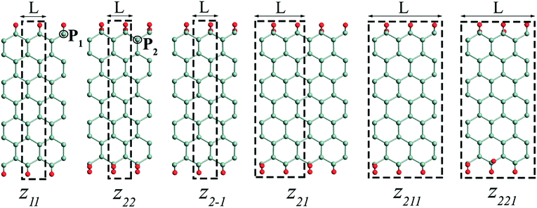
The edge functionalized AGeNRs structures studied are presented in Fig. 1. To distinguish a number of functionalized edge configurations of GeNRs “a” is used for armchair and “z” for zigzag.20 Furthermore, the subscript denotes the number of edge atoms attached to each of the edge germanium atoms along the periodic direction. To study electronic and magnetic properties, 6–19 atoms wide AGeNRs are considered. In this report, detailed theoretical predictions of AGeNR's electronic properties have been analyzed for different functionalized atoms such as hydrogen, hydro-oxide and halogens. Finally, for the B or N doping study of AGeNRs or ZGeNRs, a 7 atoms wide nanoribbon is chosen.3.1 Armchair germanene nanoribbon
| Eedge = (Eribbon − nGe × EGe − (nH/2) × EH2)/2L |
Edge functionalization is used for stabilization as the AGeNRs are unstable (+0.1953 eV Å−1) and hydrogenated structures with a22 configurations provide more stability than bare ones but with edge energies close to zero rather than negative. One can consider the hydrogenated structures metastable. Among all of the configurations, the a22 fluorinated edge functionalized ribbons are the most stable structure (−1.88 eV Å−1).
To study the effect of experimental conditions such as gas pressure and temperature, on the stability of functionalized GeNRs, the calculated edge formation energies are compared to the chemical potential (μH2) of the edge functionalizing atoms. The edge free energy μH(T,p) is calculated as follows44,45
The zero reference state of μH2(T,p) is chosen to be the total energy of an isolated edge molecule EH2 at T = 0, i.e., μH2(0,p) = EH2 ≡ 0. With respect to this reference, the pressure and temperature dependence contribution to the chemical potential is then given by44–45
| max[μH2(T,p)] = EH2 |
The lower limits are chosen for those molecule's potentials that are accessible experimentally at very high temperature (900 K).
The magnitude of the second term for hydrogen molecules at a pressure of 1 bar using ref. 46, is −1.52 eV. Consequently, the allowed range of the chemical potential, considering EH2 as the zero reference, for the hydrogen molecule is
| −1.52 < μH2(T,p) − EH2 < 0 |
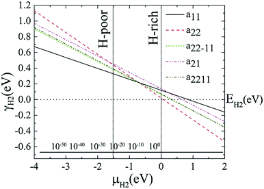
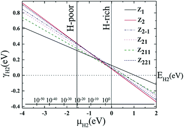
The variations of relative edge formation energy with respect to chemical potential of, for example, the H2 molecule, using EH2 as the zero reference, for different AGeNRs configurations are considered and shown in Fig. 2. Under H-poor conditions with μH2 < −1.419, a11 is feasible for AGeNRs. On the other hand, when μH2 ≥ −1.419, the a22 structure becomes more stable than other configurations. Remarkably, under ambient conditions, i.e., 300 K and 5 × 10⁻⁷ bar (μH2 = −0.694 eV), a22 has minimum energy. It's worthwhile to mention that fluorinated a22 edge structure is always the most stable structure.
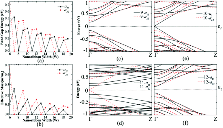
From Fig. 3(c)–(f), the band structure of germanene nanoribbons with hydrogenated edges shows a periodicity of three. This periodicity is classified into three different families where the band gaps are very small for members of the Na = 3k + 2 group, moderate for those of the Na = 3k and large for Na = 3k + 1 group. Similar periodicity is also seen for the di-hydrogenated case, but this time the band gap follows Na = 3k + 1 < Na = 3k + 2 < Na = 3k. 10-a11, which belongs to the 3k + 1 group, shows the highest band gap of 0.35 eV when mono-hydrogenated but shifted to di-hydrogenated at 11-a22. This means that almost the same band gap of mono hydrogenated ribbon can be achieved by di-hydrogenation of a wider ribbon which also offers more stability to the structure.28,34 The same periodicity behavior in band gap holds true for hydroxide group edge functionalization.
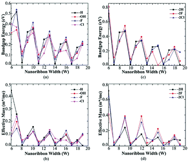
Both Fig. 4(a) and (c) show the band gap variation of AGeNRs with ribbon width. It is clear that despite being functionalized by fluorine and chlorine, they still retain the so-called family behavior seen in hydrogenated AGeNRs. The band gap periodicity in fluorine functionalized germanene nanoribbons show the same behavior as hydrogenated GeNRs. But this time the band gap is reduced drastically with increasing ribbon width because quantum confinement is substantially reduced due to electron saturation by the larger fluorine atom with a mix of sp2 and sp3 bonds providing better structural stability.
Fluorine, as opposed to hydrogen, which is covalently bonded with germanium to occupy the lowest electronic band leaving Ge–Ge bond unchanged, has higher Pauling electronegativity (3.98 eV) than that of germanium (2.01 eV) making Ge–F bond ionic. Also, a maximum band gap of 0.809 eV was found when the ribbon width was at its lowest, 6 atoms wide and fluorinated. Similar results were found for Ge–Cl bond characteristics. The values of Pauling electronegativity of X (=F, Cl) are 3.98 and 3.16, respectively, much larger than germanium.
The van der Waals radiuses of hydrogen and halogens (X = F, Cl) are 1.20, 1.47 and 1.75 Å respectively.47,48 Ge–Ge bond length (2.4 Å) in a perfect AGeNRs is almost double that of hydrogen's van der Waals radius implying that steric hindrance can be ignored in hydrogenated AGeNRs. But steric hindrance becomes acutely and prominently stronger with increasing atomic number of halogens due to increased van der Waals radius. Ionic characteristic of Ge–X bond for larger functional groups like halogens reduces electron density in the bonding orbital of Ge, deteriorating the interaction between Ge–Ge bond. Slightly deviated periodicity in band gap was found while GeNRs were functionalized with chlorine.
As the ribbon width increases, effective mass decreases dramatically and approaches almost the same value with increasing ribbon width as seen in Fig. 4(b) and (d). The decreasing effective mass offers higher mobility but at the same time the band gap decreases due to the loss of quantum confinement in the wider ribbon. Most of the edge atom functionalized configurations offer low effective masses for those greater than 9 atoms wide ribbons. Studies show that Na-AGeNRs (where Na = 6–19) are non-magnetic (NM) semiconductors and exhibit direct band gaps at the Γ point in the BZ.8
3.2 Zigzag germanene nanoribbon
The edge free energies, band gap, and magnetic states of various ZGeNRs are listed in Table S2 (see ESI†). Among all possible edge hydrogenation forms of ZGeNRs, the z21 (+0.082 eV Å−1) is found to be the most stable. However, it is about 4 times less stable than the most stable hydrogenated AGeNR (a22). The order of structure stability for different configurations of ZGeNRs is z21 > z211 > z221 > z22 > z11 > zbare. The possible reason is that Ge atoms prefer to accept a mix of sp3 hybridizations with sp2 in germanene; therefore, a mix of mono and dihydrogenation can increase the stability of the structures. In addition, similar to AGeNRs, halogenating would increase the stability of the ZGeNRs. The stability of fluorinated z22 (−1.66 eV Å−1) is more stable than the hydrogenated z22 (0.107 eV Å−1).
Similar to AGeNRs, the stability of halogenated ZGeNRs decreases with increasing atomic number of halogen atoms. In order to account for the experimental conditions, the Gibbs free energies of the aforementioned hydrogenated edge structures are calculated and plotted in Fig. 6. For low hydrogen chemical potential μH2 < −1.5 eV, the z11 has minimum energy. When −1.5 eV ≤ μH2 < −0.5 eV, several different edge structures have almost the same amount of energy. Further increase of μH2 up to +2.0 eV finds z22 most favorable.
3.3 Armchair germanene nanoribbons doped by N or B atoms
The effects of doping on band gap as well as magnetic properties of GeNRs with N or B impurity have been investigated. Theoretically, it is possible to replace the Ge atoms in different sites of the nanoribbon using a single N or B. Formation energy (Ef) of the nanoribbon with an N or B impurity is calculated to further examine which site is experimentally more likely to occur,| Ef = Edoped − (Epristine − (m + n)EGe + mEN + nEB) |
Formation energies, band gaps, and magnetic edge states of hydrogenated and fluorinated AGeNRs doped with N or B atom are listed in Table S1.† The formation energy of B doped AGeNRs is found to be lower than that of N-doped AGeNRs, suggesting that the B impurity is easier to substitute than Ge atoms at the edge of AGeNRs. It can also be due to the larger Pauling electronegativity (3.04) and smaller covalent radius (0.75 Å) of the N impurity compared to the B impurity (Pauling electronegativity of 2.04 and covalent radius of 0.82 Å).47 The optimized N–Ge (1.85 Å) and N–H (1.02 Å) bonds for N doping at the edge are found to be shorter than B–Ge (1.99 Å) and B–H (1.21 Å) bonds for B doping at the same edge location.
Because of the smaller ionic radius and shorter bond length of N doping compared to B doping in GeNRs, the lattice distortion of the latter is more pronounced than that of the former. It appears that B doped AGeNRs have almost the same bond length as the pristine ones and offer a more stable structure with less lattice distortion.
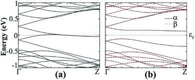
The band structures of N- or B-doped AGeNRs show that there is a half-filled band near the Fermi level, resulting in a semiconductor–metal transition, as seen in Fig. 8(b) and (d). It is interesting to find that the band introduced by an N dopant lies closer to the conduction band, while the band induced by a B dopant is located near valence band. The reason behind this is that the value of ionic electronegativity of the Ge atom is very close to B and lower than N. Hence the orbit energies of B are higher than those of Ge and lower for N than Ge. As a result, the B (N) impurity shifts the band levels of GeNRs up (down).51,53
 | ||
| Fig. 8 Band structure of B-doped fluorinated a11 in the (a) NM and (b) FM states, N-doped fluorinated a11 in the (c) NM and (d) FM states. | ||
The spin-polarized calculations of fluorinated a11 doped with a B atom indicate that it is semiconducting in both channels with band gaps of 0.425 and 0.393 eV for spin-up and spin-down channels, respectively, as seen in Fig. 8(b). Fig. 8(d) shows the spin-polarized band structure of N-doped fluorinated a11. Interestingly enough, the valence band maximum (VBM) of the spin-up channel and the conduction band minimum (CBM) of the spin-down channel are both close to the Fermi level. An indirect band gap of 0.136 eV was found in the spin up channel and a direct band gap of 0.439 eV was found in spin down channel for the fluorinated a11 doped with N atom. Besides, the hydrogenated a11 doped with N or B atom is still metallic. As found from calculation, when the impurity atom (N or B) is replaced with Ge atoms at the edge, the spins on the edge are locally suppressed around the dopant atom and remain less affected on the undoped edge. As a consequence, a total magnetic moment of 0.761 μB (or 0.583 μB) per supercell is gained for the B doped (or N doped).
The spin resolved band structure of N- or B-doped hydrogenated z11 shows that the introduction of dopants at the edges give rise to asymmetrical spin-up and spin-down bands around εf, suggesting that the spin degeneracy of AFM – z11 disappeared and the mirror symmetry is broken.
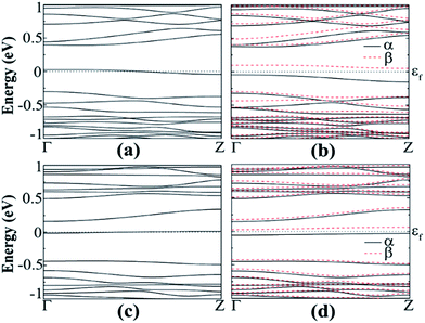
The spin polarized calculation of hydrogenated a11 doped with N next to the edge atom (P2) of the nanoribbon shows that it is AFM semiconducting in both channels with band gaps of 0.230 and 0.414 eV for spin-up and spin-down channels, respectively as can be seen from Fig. 9(b). On the contrary, fluorinated a11 doped with N at the same position shows FM semiconducting behavior in both channels. The band gap in this case, is 0.204 eV, which is direct band gap in spin-up channel but indirect in spin-down channel with 0.483 eV as shown in Fig. 9(d). The total magnetic moment was calculated to be 0.768 μB in this case.
 | ||
| Fig. 9 Band structure of N-doped hydrogenated a11 in the (a) NM and (b) AFM states, N-doped fluorinated (c) NM and (d) FM states. | ||
For higher doping concentrations, a new band appears close to valence (conduction) band for each additional boron (nitrogen) atom. Spin polarized calculations show that hydrogenated a11 doped with double or triple boron atoms are metal, similar to single doped case, as shown in Fig. 10. When AGeNRs are doped by a higher concentration of nitrogen, no significant change was found except for the double nitrogen doped case. It shows semiconducting behavior with an indirect band gap of 0.241 eV. These results are similar to previous findings for silicene nanoribbons.52
 | ||
| Fig. 10 Effect of doping concentration: band structure of hydrogenated a11 when doped by (a) B, (b) 2B and (c) 3B. | ||
3.4 Doped zigzag germanene nanoribbons
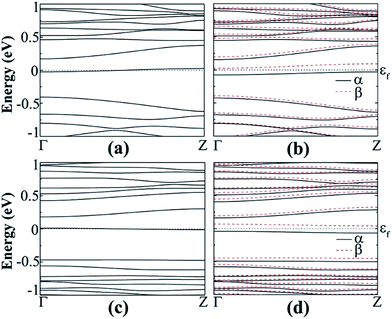
The doping effects on ZGeNRs are considered. In this case 7-ZGeNR is used for the supercell model containing 42 germanium atoms and 6 or 12 atoms of hydrogen or fluorine is selected. The doping position is chosen at the edge of the nanoribbon to substitute a Ge atom because of its low formation energy. This ensures the structural stability of ZGeNRs possibly due to the decay of high energy states in GeNRs, as reported for SiNRs.49 The non-spin-polarized calculation shows that doped ZGeNRs are all metallic. Formation energies, band gaps, and magnetic edge states of hydrogenated and fluorinated ZGeNRs doped with N or B atom are listed in Table S3.†For the hydrogenated B-doped case, the spin-up channel shows semiconducting behavior with a direct band gap of 0.314 eV and the spin-down channel is still metallic respectively, as shown in Fig. 11(b). But in the case of N doping, the spin-down channel is AFM semiconducting with direct band gap of 0.333 eV and the spin-up channel is metallic. The unpaired spin-up π band and spin-down π* band at the edge of the nanoribbons is believed to be the origin of spin-degeneracy in pristine hydrogenated z11.
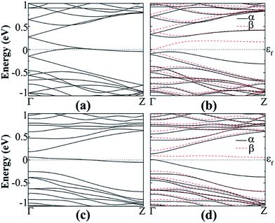 | ||
| Fig. 11 Band structure of B-doped hydrogenated z11 in the (a) NM and (b) AFM states and N-doped hydrogenated (c) NM and (d) AFM states. | ||
N or B doping at the edge of the ZGeNR provides an additional electron or hole to the GeNR that can occupy the unpaired spin orbital, causing the band's degeneracy to break. Injection of extra electrons and holes into the edge of the π and π* states more than interior states can be related to the local structural distortion caused by impurities at the edge of the nanoribbon.51,53
In the case of hydrogenated z22 when doped with B, it transforms to a half metallic semiconductor with a band gap of 0.351 eV in the spin-down channel [Fig. 12(b)] and shows total magnetic momentum of 0.907 μB in the FM state. But for fluorinated B doped, it transforms to AFM semiconductor for both of the channels with a band gap of 0.101 eV (direct) and 0.173 eV (indirect) in the spin-up and spin-down channel respectively [Fig. 12(d)]. By comparing formation energies for both of the structures, it can be seen that the fluorinated (Ef = −4.62 eV) is more stable than the hydrogenated (Ef = −3.95 eV). The reason can be that the Pauling electronegativity of fluorine (3.98) is higher than hydrogen (2.2) and also the bond length of Ge–F (1.78 Å) is very near the Ge–Ge bond (2.4 Å).47
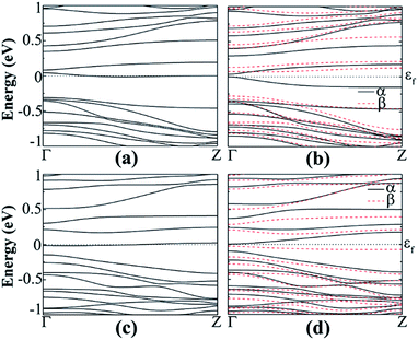 | ||
| Fig. 12 Band structure of B-doped hydrogenated z22 in the (a) NM and (b) FM states, B-doped fluorinated (c) NM and (d) AFM states. | ||
Finally, the effect of doping concentration on electronic and magnetic properties is studied for z11. It is found that double boron and nitrogen doped ZGeNR show semiconducting behavior with very small band gaps of 0.01 eV and 0.078 eV, respectively. Spin polarized calculations also show that triple boron/nitrogen doped z11 are NM materials.
4 Conclusions
Electronic and magnetic properties of edge functionalized (–H, –OH, –F, –Cl) AGeNRs and ZGeNRs were investigated using first principle calculations based on DFT. It was found that the halogenated structures are more stable than hydrogenated or hydroxide structures though stability decreases with increasing atomic number of halogens. Moreover, halogens still ensure more stable structures than other functionalized atoms in any case. Quantum confinement was also retained even when functionalized with other atoms rather than hydrogenated only.This study showed that the energy band gap changes are strongly dependent on the armchair nanoribbon's width, edge atom functionalization and the number of functionalizing atoms at the edges. Edge functionalization can be used for energy band gap tuning (0.01–0.84 eV) of AGeNRs. Depending on the type of edge functionalization, the same band gap with wider ribbons can be achieved.
Formation energy studies revealed, regardless of impurity atoms (N or B) in AGeNRs or ZGeNRs, dopants preferred to be on the edges. Single atom doped AGeNRs at one edge becomes metallic due the appearance of a half-filled impurity atom induced band which enables them to be used in negative differential resistance devices. Single atom doping (N or B) suppresses the spin polarization of the doped edges transforming it from an AFM ground state to FM. Lastly, formation and edge free energy studies revealed the feasibility of chemical synthetization of edge functionalized germanene.
References
- K. S. Novoselov, A. K. Geim, S. V. Morozov, D. Jiang, M. I. Katsnelson, I. V. Grigorieva, S. V. Dubonos and A. A. Firsov, Nature, 2005, 438, 197–200 CrossRef CAS PubMed.
- K. S. Novoselov, A. K. Geim, S. V. Morozov, D. Jiang, Y. Zhang, S. V. Dubonos, I. V. Grigorieva and A. A. Firsov, Science, 2004, 306, 666–669 CrossRef CAS PubMed.
- J. Bai, X. Zhong, S. Jiang, Y. Huang and X. Duan, Nat. Nanotechnol., 2010, 5, 190–194 CrossRef CAS PubMed.
- Y. Son, M. L. Cohen and S. G. Louie, Phys. Rev. Lett., 2006, 97, 216803 CrossRef PubMed.
- M. Y. Han, B. Ozyilmaz, Y. Zhang and P. Kim, Phys. Rev. Lett., 2007, 98, 206805 CrossRef PubMed.
- K. Takeda and K. Shiraishi, Phys. Rev. B: Condens. Matter Mater. Phys., 1994, 50, 14916 CrossRef CAS.
- S. Cahangirov, M. Topsakal, E. Aktürk, H. Şahin and S. Ciraci, Phys. Rev. Lett., 2009, 102, 236804 CrossRef CAS PubMed.
- Q. Pang, Y. Zhang, J. M. Zhang, V. Ji and K. W. Xu, Nanoscale, 2011, 3, 4330 RSC.
- H. Şahin, S. Cahangirov, M. Topsakal, E. Bekaroglu, E. Akturk, R. T. Senger and S. Ciraci, Phys. Rev. B: Condens. Matter Mater. Phys., 2009, 50, 155453 CrossRef.
- N. J. Roome and J. D. Carey, ACS Appl. Mater. Interfaces, 2014, 6, 7743–7750 CAS.
- P. Liang, Y. Liu, S. Xing, H. Shu and B. Tai, Solid State Commun., 2016, 226, 19–24 CrossRef CAS.
- L. Li, S. Lu, J. Pan, Z. Qin, Y. Wang, Y. Wang, G. Cao, S. Du and H. Gao, Adv. Mater., 2014, 26, 4820–4824 CrossRef CAS PubMed.
- H. Oughaddou, S. Sawaya, J. Goniakowski, B. Aufray, G. Le Lay, J. M. Gay, G. Tréglia, J. P. Bibérian, N. Barrett, C. Guillot, A. Mayne and G. Dujardin, Phys. Rev. B: Condens. Matter Mater. Phys., 2000, 62, 16653 CrossRef CAS.
- M. Derivaz, D. Dentel, R. Stephan, M. Hanf, A. Mehdaoui, P. Sonnet and C. Pirri, Nano Lett., 2015, 15, 2510–2516 CrossRef CAS PubMed.
- E. Bianco, S. Butler, S. Jiang, O. D. Restrepo, W. Windi and J. E. Goldberger, ACS Nano, 2013, 7, 414–4421 Search PubMed.
- M. E. Dávila, L. Xian, S. Cahangirov, A. Rubio and G. Le Lay, New J. Phys., 2014, 16, 095002 CrossRef.
- S. Jiang, S. Butler, E. Bianco, O. D. Restrepo, W. Windl and J. E. Goldberger, Nat. Commun., 2014, 5, 3389 Search PubMed.
- L. Zhang, P. Bampoulis, A. N. Rudenko, Q. Yao, A. van Houselt, B. Poelsema, M. I. Katsnelson and H. J. W. Zandvliet, Phys. Rev. Lett., 2016, 116, 256804 CrossRef CAS PubMed.
- M. Kan, J. Zhou, Y. Li and Q. Sun, Appl. Phys. Lett., 2012, 100, 173106 CrossRef.
- M. Kan, J. Zhou, Q. Sun, Q. Wang, Y. Kawazoe and P. Jena, Phys. Rev. B: Condens. Matter Mater. Phys., 2012, 85, 155450 CrossRef.
- T. Wassmann, A. P. Seitsonen, A. M. Saitta, M. Lazzeri and F. Mauri, Phys. Rev. Lett., 2008, 101, 096402 CrossRef PubMed.
- G. Lee and K. Cho, Phys. Rev. B: Condens. Matter Mater. Phys., 2009, 79, 165440 CrossRef.
- K. A. Ritter and J. W. Lyding, Nat. Mater., 2009, 8, 235 CrossRef CAS PubMed.
- S. Bhandary, O. Eriksson, B. Sanyal and M. I. Katsnelson, Phys. Rev. B: Condens. Matter Mater. Phys., 2010, 82, 165405 CrossRef.
- J. Kunstmann, C. Özdoğan, A. Quandt and H. Fehske, Phys. Rev. B: Condens. Matter Mater. Phys., 2011, 83, 045414 CrossRef.
- P. Wagner, C. P. Ewels, V. V. Ivanovskaya, P. R. Briddon, A. Pateau and B. Humbert, Phys. Rev. B: Condens. Matter Mater. Phys., 2011, 84, 134110 CrossRef.
- X. H. Zheng, X. L. Wang, L. F. Huang, H. Hao, J. Lan and Z. Zeng, Phys. Rev. B: Condens. Matter Mater. Phys., 2012, 86, 081408 CrossRef.
- P. Wagner, C. P. Ewels, J. J. Adjizian, L. Magaud, P. Pochet, S. Roche, A. Lopez-Bezanilla, V. V. Ivanovskaya, A. Yaya and M. Rayson, J. Phys. Chem. C, 2013, 117, 26790–26796 CAS.
- C. Si, J. Liu, Y. Xu, J. Wu, B. L. Gu and W. Duan, Phys. Rev. B: Condens. Matter Mater. Phys., 2014, 89, 115429 CrossRef.
- Z. Ni, Q. Liu, K. Tang, J. Zheng, J. Zhou, R. Qin and Z. Gao, Nano Lett., 2012, 12(1), 113–118 CrossRef CAS PubMed.
- B. V. D. Broek, M. Houssa, E. Scalise, G. Pourtois, V. V. Afanas'ev and A. Stesmans, Appl. Surf. Sci., 2014, 291, 104 CrossRef.
- W. Xia, W. Hu, Z. Li and J. Yang, Phys. Chem. Chem. Phys., 2014, 16, 22495 RSC.
- Y. He, P. Zhang, X. Hou, J. Xu, M. Wang, Y. Wu, J. Qu and M. Dong, RSC Adv., 2014, 4, 35042 RSC.
- S. M. Aghaei and I. Calizo, J. Appl. Phys., 2015, 118, 104304 CrossRef.
- S. M. Aghaei and I. Calizo, Conf. Proc.–IEEE Southeastcon, 2015, 1–6 CAS.
- S. M. Aghaei, M. M. Monshi, I. Torres and I. Calizo, RSC Adv., 2016, 6, 17046 RSC.
- Atomistix ToolKit version 2014.1, QuantumWise A/S, http://www.quantumwise.com Search PubMed.
- M. Brandbyge, J. L. Mozos, P. Ordejón, J. Taylor and K. Stokbro, Phys. Rev. B: Condens. Matter Mater. Phys., 2002, 65, 165401 CrossRef.
- J. M. Soler, E. Artacho, J. D. Gale, A. García, J. Junquera, P. Ordejón and D. Sánchez-Portal, J. Phys.: Condens. Matter, 2002, 14, 2745 CrossRef CAS.
- J. P. Perdew, K. Burke and M. Ernzerhof, Phys. Rev. Lett., 1996, 77, 3865 CrossRef CAS PubMed.
- S. M. Aghaei, M. M. Monshi and I. Calizo, RSC Adv., 2016, 6, 94417–94428 RSC.
- J. Prasongkit, R. G. Amorim, S. Chakraborty, R. Ahuja, R. H. Scheicher and V. Amornkitbamrung, J. Phys. Chem. C, 2015, 119, 16934–16940 CAS.
- P. Wagner, V. V. Ivanovskaya, M. Melle-Franco, B. Humbert, J. Adjizian, P. R. Briddon and C. P. Ewels, Phys. Rev. B: Condens. Matter Mater. Phys., 2013, 88, 094106 CrossRef.
- K. Reuter and M. Scheffler, Phys. Rev. B: Condens. Matter Mater. Phys., 2002, 65, 035406 CrossRef.
- G. Soldano, F. Juarez, B. Teo and E. Santos, Carbon, 2014, 78, 181 CrossRef CAS.
- D. R. Stull and H. Prophet, JANAF Thermochemical Tables, U.S. National Bureau of Standards, Washington, DC, 2nd edn, 1971 Search PubMed.
- http://www.webelements.com.
- G. G. Guzman-Verri and L. C. L. Y. Voon, J. Phys.: Condens. Matter, 2011, 23, 145502–145506 CrossRef CAS PubMed.
- F. B. Zheng, C. W. Zhang, P. J. Wang and S. S. Li, J. Appl. Phys., 2013, 113, 154302 CrossRef.
- J. M. Zhang, W. T. Song, K. W. Xu and V. Ji, Comput. Mater. Sci., 2014, 95, 429 CrossRef CAS.
- H. X. Luan, C. W. Zhang, F. B. Zheng and P. J. Wang, J. Phys. Chem. C, 2013, 117, 13620–13626 CAS.
- L. Ma, J. M. Zhang, K. W. Xu and V. Ji, Phys. B, 2013, 425, 66–71 CrossRef CAS.
- F. B. Zheng, C. W. Zhang, S. S. Yan and F. Li, J. Mater. Chem. C, 2013, 1, 2735 RSC.
Footnote |
| † Electronic supplementary information (ESI) available. See DOI: 10.1039/c6ra25083a |
| This journal is © The Royal Society of Chemistry 2017 |


