 Open Access Article
Creative Commons Attribution 3.0 Unported Licence
A novel wide-spectrum response hexagonal YFeO3 photoanode for solar water splitting†
Yongsheng Guoa,
Ningsi Zhanga,
Huiting Huanga,
Zhaosheng Li *a and
Zhigang Zouab
aCollaborative Innovation Center of Advanced Microstructures, National Laboratory of Solid State Microstructures, College of Engineering and Applied Sciences, Nanjing University, 22 Hankou Road, Nanjing, 210093, People's Republic of China. E-mail: zsli@nju.edu.cn
bJiangsu Key Laboratory for Nano Technology, Department of Physics, Nanjing University, 22 Hankou Road, Nanjing, 210093, People's Republic of China
First published on 27th March 2017
Abstract
Nanoparticle-assembled films of hexagonal YFeO3 with a wide-spectrum response were prepared by electrophoretic deposition. Hexagonal YFeO3, with the band gap of 1.88 eV, was found to exhibit photoelectrochemical water splitting.
Photoelectrochemical (PEC) water splitting is a promising approach to capture and store the abundant solar energy in hydrogen as a renewable and environmentally friendly fuel.1,2 Water oxidation is a limiting-step for the water splitting reaction. The bottleneck of PEC water splitting is a lack of efficient and stable photoanodes. Over the past few decades, iron-based oxide semiconductors, specially hematite, have been intensively studied for PEC water oxidation, due to the favourable band gap, cheap price, and high stability toward long-term operation.3,4 However, a hematite photoanode was often limited by its intrinsic material properties, such as low charge carrier mobility, short photoexcited charge carrier lifetime and slow oxygen evolution reaction kinetics.5,6 Since theoretical solar-to-hydrogen efficiency of photoanodes depends on their bandgap absorption edges, it is meaningful to develop new iron-based oxide photoanodes with wide-spectrum response. However, there are very limited reports about novel iron-based oxide photoanodes.7,8
Here, we have reported for the first time that hexagonal YFeO3 (h-YFeO3) with wide-spectrum response acts as a photoanode material for solar water splitting. Compared with hematite and o-YFeO3 photoanodes, h-YFeO3 has smaller band gap (approximately 1.85–1.9 eV), thus exhibiting higher theoretical solar-to-hydrogen efficiency (approximately 20%).
In this study, h-YFeO3 and o-YFeO3 nanoparticles were synthetized via a facile sol–gel method (Experimental, in the ESI†). Nanoparticle-assembled YFeO3 films with a transparent conductive substrate of F:SnO2 glass (fluorine-doped tin oxide, FTO) were fabricated by electrophoretic deposition, followed by necking post treatment and air annealing in muffle furnace. A brief schematic illustration of the photoelectrode preparation procedure is shown in Scheme S1 (details in ESI†). Nanoparticle-assembled hematite photoanodes prepared in the same method have no obvious advantage compared with h-YFeO3, as shown in Fig. S1.† As-prepared h-YFeO3 nanoparticle-assembled films have a saturation water-splitting photocurrent of approximately 0.08 mA cm−2 and a noticeable onset potential of 0.95 V vs. RHE (reversible hydrogen electrode), which is smaller than the onset potential of hematite.9
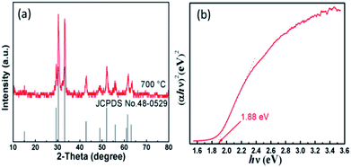
The hexagonal and orthorhombic phases of YFeO3 can be controlled by different calcined temperatures. According to the result of TG-DSC shown in Fig. S2,† there is an obvious exothermic peak at the temperature of 410 °C to 450 °C, which indicates that the combustion of organic matter releases large amounts of heat. There is another peak at the temperature of 760 °C, which may be described as the phase transition temperature of hexagonal to orthorhombic. After annealing at 700 °C and 800 °C for 3 h in air, h-YFeO3 and o-YFeO3 were obtained, respectively (Fig. S3, ESI†). The XRD pattern of the as-prepared h-YFeO3 nanoparticles is shown in Fig. 1(a). All the peaks are assigned to h-YFeO3 (JCPDS card no. 48-0529), which suggests that no impurity phases are observed and the pure phase h-YFeO3 sample is prepared. After the h-YFeO3 nanoparticle-assembled films were annealed at 650 °C for 1 hour and then 700 °C for 10 min, there is no impurity phases (as shown in Fig. S4†), suggesting that there is no phase transition during the annealing process.
 | ||
| Fig. 1 (a) XRD pattern of h-YFeO3 nanoparticles and (b) Tauc plot for h-YFeO3 obtained from UV-vis absorption spectra. | ||
UV-vis absorption spectra (Fig. S5 and S6, ESI†) of YFeO3 power were measured by diffuse reflectance spectroscopy by using the Kubelka–Munk function. The absorption edges of h-YFeO3 and o-YFeO3 are around 660 nm and 600 nm, respectively. For a semiconductor, the optical absorption behaviours depend on the types of semiconductor. A photon of energy can produce an electron–hole pair in a direct band gap semiconductor quite easily, because the electron does not need to be given very much momentum. However, an electron must undergo a significant change in its momentum for a photon of energy to produce an electron–hole pair in an indirect band gap semiconductor. It requires such an electron to interact not only with the photo to gain energy, but also with a lattice vibration called a phonon in order to either gain or lose momentum. The indirect process proceeds at a much slower rate, as it requires three entities to intersect in order to proceed: an electron, a photon and a phonon. Hence, the optical absorption spectrum curve of the direct band gap semiconductor is steep. However, the optical absorption spectrum curve of the indirect band gap semiconductor is gentle. In conclusion, according to the UV-vis absorption spectra of different phases composition, o-YFeO3 shows a behaviour of indirect semiconductor, while h-YFeO3 is a direct semiconductor. Hence, the characteristics of semiconductor indicate the direct nature and narrowing of band gap ensure the higher absorbance values and wider spectrum of absorbance.10 Moreover, the transfer processes at the semiconductor/electrolyte interface of two types of charge transfer mechanisms of different types of semiconductors are also showing that h-YFeO3 is a more suitable candidate.11 The Tauc plot in Fig. 1(b), suggests its band gap is approximate to 1.88 eV, in agreement with the reported value.12
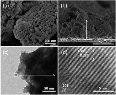
The morphology and microscopic structure of the nanoparticle-assembled h-YFeO3 films were observed by scanning electron microscopy (SEM) and transmission electron microscopy (TEM). As shown in Fig. 2(a), the surface of the nanoparticle-assembled film shows a porous structure with a large number of internal spaces. The cross-sectional image shows that the thickness of the nanoparticle-assembled film is about 1.8 μm and it has a porous structure accumulated by small nanoparticles over the whole h-YFeO3 photoelectrode (details can be seen in Fig. S7, ESI†). According to the molecular formula of h-YFeO3, its stoichiometric ratio of Y and Fe is 1![[thin space (1/6-em)]](https://www.rsc.org/images/entities/char_2009.gif) :
:![[thin space (1/6-em)]](https://www.rsc.org/images/entities/char_2009.gif) 1, which is consistent with the result of energy dispersive spectrometer (EDS) measurement (Fig. S9, ESI†). The Ti appeared in EDS-mapping image comes from the TiCl4 post treatment. Fig. 2(c) presents the TEM image of h-YFeO3 and Fig. S8† gives the distribution of particle sizes obtained after annealing the sol–gel precursor. Statistical analysis of the sample by SEM (Fig. S7(a), ESI†) and TEM (Fig. S8, ESI†) suggested that a mean particle size was identified to be 40 (±10) nm. The high-resolution TEM image of Fig. 2(d) shows the particles with continuous lattice fringes originating from the (1 0 1) plane with a d-spacing of 0.286 nm, which clearly indicated the existence of h-YFeO3. The porous nanoparticle-assembled films could not only increase the light absorption caused by interactions between the porous structure and the exposed light, but also provide more effective reactive sites for the reactions to take place and facilitate the electrolyte diffusion onto the surface of the electrode,13 resulting in the enhancement of PEC properties.
1, which is consistent with the result of energy dispersive spectrometer (EDS) measurement (Fig. S9, ESI†). The Ti appeared in EDS-mapping image comes from the TiCl4 post treatment. Fig. 2(c) presents the TEM image of h-YFeO3 and Fig. S8† gives the distribution of particle sizes obtained after annealing the sol–gel precursor. Statistical analysis of the sample by SEM (Fig. S7(a), ESI†) and TEM (Fig. S8, ESI†) suggested that a mean particle size was identified to be 40 (±10) nm. The high-resolution TEM image of Fig. 2(d) shows the particles with continuous lattice fringes originating from the (1 0 1) plane with a d-spacing of 0.286 nm, which clearly indicated the existence of h-YFeO3. The porous nanoparticle-assembled films could not only increase the light absorption caused by interactions between the porous structure and the exposed light, but also provide more effective reactive sites for the reactions to take place and facilitate the electrolyte diffusion onto the surface of the electrode,13 resulting in the enhancement of PEC properties.
 | ||
| Fig. 2 SEM images of h-YFeO3 deposited on FTO glass (a) the top view and (b) the cross-section view; (c) TEM image of h-YFeO3; (d) HRTEM image of the square area of h-YFeO3 showing lattice fringes. | ||
To further analyse the properties of electronic structure of the h-YFeO3, electrochemical impedance measurements were carried out. The conducting type and flat-band potential of h-YFeO3 can be calculated using the Mott–Schottky equation2,14
| 1/C2 = (2/e0εε0N)[(VFB − V) − kT/e0] |
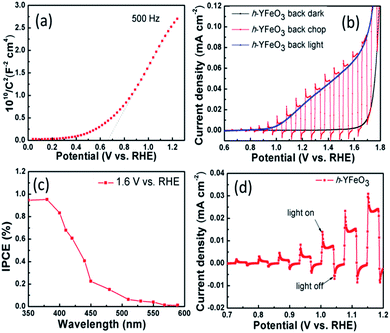
One can demonstrate that h-YFeO3 is an n-type semiconductor, according to the slope of the linear region in its Mott–Schottky plot as illustrated in Fig. 3(a). The flat-band potential of the h-YFeO3 was estimated to be 0.68 V vs. RHE. The PEC performance of the nanoparticle-assembled photoanode films were tested in a three-electrode system using an electrochemical analyzer (CHI-660D, Shanghai Chenhua, China) in 1 M NaOH aqueous solution (pH = 13.6) under AM 1.5 G simulated sunlight for illumination from back side (glass side) of FTO (100 mW cm−2). Linear sweep voltammograms for the h-YFeO3 and o-YFeO3 photoelectrodes under chopped light (Fig. S10, ESI†) show that the h-YFeO3 electrode has a better photoresponse than that of o-YFeO3 electrode. To explain the different PEC performances of the two types of photoelectrodes, the SEM images of the electrodes for different phases were compared. The results (Fig. S7, ESI†) indicate that the particle size of o-YFeO3 is larger than that of h-YFeO3 and it is more compact between particles of o-YFeO3, which could account for its lower PEC performance. Besides, the results of PEC performances are in good agreement with the analysis of Fig. 1(b). As shown in Fig. 3(b), the photocurrent density of h-YFeO3 is about 0.025 mA cm−2 at 1.23 V vs. RHE, and the saturation photocurrent is approximately 0.08 mA cm−2.
The IPCE spectra were measured with a Xe lamp as the light source to evaluate the spectral response for water oxidation. The monochromatic light was obtained by Xe lamp passed through a monochromator from 350 nm to 589 nm. Chronoamperometry was operated at a constant potential (1.6 V vs. RHE). Fig. 3(c) shows that the shape of the IPCE curve generally follows the trend of the UV-vis absorption spectra of the electrode (Fig. S5, ESI†) which means that the PEC water oxidation is indeed derived from the light absorption. The visible photocurrent onset is located at 568 nm, and the maximum value of IPCE increases to 0.95% with the decrease of wavelength.
As shown in Fig. 3(d), the photocurrents under chopped illumination at low bias, suggest that there are obvious transient photocurrents. The transient photocurrent was also measured at a potential of 1.6 V vs. RHE under AM 1.5 G illumination (100 mW cm−2) (Fig. S11, ESI†). When the light is turned on, photogenerated holes move to the electrode surface, and fill surface states and/or react with water. Immediately, slow photocurrent decay with time is observed. When the light is switched off, electrons begin to recombine with holes stored in surface states.14,15 It illustrates serious trapping and discharging effects for the charge carriers. To further demonstrate the possible reasons to enhance PEC performance of the nanoparticle-assembled h-YFeO3 photoanode, 0.5 M H2O2 was added into the electrolyte as a hole scavenges. We can observe a cathodic shift of onset potential and an increase of photocurrent (Fig. S12, ESI†) because the photogenerated holes in the h-YFeO3 transferred from the bulk to the surface more easily and the electron/hole recombination was reduced.15–17
One of the vital factors for future practical applications of the photoelectrode materials is photochemical stability. Consequently, the stability of the nanoparticle-assembled h-YFeO3 electrode was tested (Fig. S13, ESI†). A little decay in the photocurrent density is observed, which confirms the stability of the h-YFeO3 electrode.
In conclusion, we have reported a new photoanode material, h-YFeO3, for solar water splitting. It has shown obvious PEC performance with a saturation photocurrent about 0.08 mA cm−2 and a noticeable onset potential of 0.95 V vs. RHE. The h-YFeO3 is a promising photoanode material for solar water splitting in the future, due to its direct band gap and theoretical solar-to-hydrogen efficiency of approximately 20%.
Acknowledgements
This work was supported by National Basic Research Program of China (973 Program, 2013CB632404), a Project Funded by the Priority Academic Program Development of Jiangsu Higher Education Institutions, and National Natural Science Foundation of China (21473090 and U1663228).Notes and references
- A. Fujishima and K. Honda, Nature, 1972, 238, 37 CrossRef CAS PubMed.
- M. G. Walter, E. L. Warren, J. R. McKone, S. W. Boettcher, Q. X. Mi, E. A. Santori and N. S. Lewis, Chem. Rev., 2010, 110, 6446 CrossRef CAS PubMed.
- S.-H. Cho, J.-W. Jang, L. G. Li, J. Jian, H. Y. Wang and J. L. MacManus-Driscoll, Chem. Mater., 2016, 28, 3017 CrossRef CAS PubMed.
- J. Y. Cao, T. Kako, P. Li, S. X. Ouyang and J. H. Ye, Electrochem. Commun., 2011, 13, 275 CrossRef CAS.
- K. Sivula, F. Le Formal and M. Grätzel, ChemSusChem, 2011, 4, 432 CrossRef CAS PubMed.
- A. Kay, I. Cesar and M. Grätzel, J. Am. Chem. Soc., 2006, 128, 15714 CrossRef CAS PubMed.
- M. A. Butler, D. S. Ginley and M. Eibschutz, J. Appl. Phys., 1977, 48, 3070 CrossRef CAS.
- J. H. Kim, Y. J. Jang, J. H. Kim, J.-W. Jang, S. H. Choi and J. S. Lee, Nanoscale, 2015, 7, 19144 RSC.
- O. Zandi, B. M. Klahr and T. W. Hamann, Energy Environ. Sci., 2013, 6, 634 CAS.
- J. Kocher, A. Kumar, A. Kumar, S. Priya and J. Kumar, Phys. Status Solidi B, 2014, 251, 1552 CrossRef CAS.
- L. Bertoluzzi, P. Lopez-Varo, J. A. Jiménez Tejada and J. Bisquert, J. Mater. Chem. A, 2016, 4, 2873 CAS.
- J. Liu, F. He, L. X. Chen, X. Q. Qin, N. Q. Zhao, Y. Huang and Y. T. Peng, Mater. Lett., 2016, 165, 263 CrossRef CAS.
- X. Wen, W. J. Luo and Z. G. Zou, J. Mater. Chem. A, 2013, 1, 15479 CAS.
- D. W. Kim, S. C. Riha, E. J. DeMarco, A. B. F. Martinson, O. K. Farha and J. T. Hupp, ACS Nano, 2014, 8, 12199 CrossRef CAS PubMed.
- P. Salvador, M. L. García González and F. Muñoz, J. Phys. Chem., 1992, 96, 10349 CrossRef CAS.
- V. Noack, H. Weller and A. Eychmüller, Phys. Chem. Chem. Phys., 2003, 5, 384 RSC.
- Y. M. Ma, S. R. Pendlebury, A. Reynal, F. Le Formal and J. R. Durrant, Chem. Sci., 2014, 5, 2964 RSC.
Footnote |
| † Electronic supplementary information (ESI) available: Experimental details including fabrication methods, schematic illustration, XRD, UV-vis, SEM images, i–t curve, etc. See DOI: 10.1039/c6ra28390j |
| This journal is © The Royal Society of Chemistry 2017 |

