
 Open Access Article
 This Open Access Article is licensed under a
 Creative Commons Attribution 3.0 Unported Licence
Facile synthesis of self-aligned gold nanoparticles by crack templated reduction lithography†
Min-Cheol Lim a,
Sae-Hyung Kimb,
Kisang Parkab,
Young-Rok Kimc,
Jae-Ho Kimb,
Gyeongsik Oka and
Sung-Wook Choi*a
a,
Sae-Hyung Kimb,
Kisang Parkab,
Young-Rok Kimc,
Jae-Ho Kimb,
Gyeongsik Oka and
Sung-Wook Choi*a
aFood Safety Research Group, Korea Food Research Institute, Sungnam 13539, Korea. E-mail: swchoi@kfri.re.kr; Fax: +82 31 709 9876; Tel: +82 31 780 9327
bDepartment of Molecular Science and Technology, Ajou University, Suwon 16499, Korea
cGraduate School of Biotechnology, Department of Food Science and Biotechnology, Kyung Hee University, Yongin 17104, Korea
First published on 27th February 2017
Abstract
Fabrication of 1D gold nanoparticle (NP) arrays by crack templated reduction lithography (CTRL) is demonstrated. The gold NPs are synthesized in situ on the cracks in a polydimethoxysiloxane (PDMS) substrate without additional reducing/stabilizing agents. Upon directionally bending the substrate, various array patterns formed on the PDMS rubber.
Highly aligned gold nanoparticles (NPs) and nanowires (NWs) have attracted considerable interest owing to their diverse applications in electrical1–4 and optical sensors.5–7 Enormous efforts have been devoted to producing aligned gold NPs and NWs on a large scale. Electrodeposition of metal NWs in a confined region, such as anodized anodic membranes, and the synthesis of metal NPs by reducing agents are well-known conventional solution processes to prepare metal NWs and NPs.1,2,8–11 Although these approaches can produce large quantities, their applications are restricted when the NPs and NWs must be aligned on a solid surface because this alignment requires additional transfer processes. In situ synthesis methods on solid surfaces have also been investigated, including lithographically patterned electrodeposition,12,13 microstructured template-guided methods,14–16 and biomolecule-templated methods.17–20 Currently, these approaches enable the preparation of selectively aligned NPs and NWs, but obtaining a highly aligned 1D array of NPs and NWs without using an additional nano- or microstructure patterned substrate is difficult. Hence, a simple route for the preparation of 1D arrays of NPs and NWs on solid surfaces is still required to achieve selective alignment, diverse patterns, and size control.
Herein, we report a novel synthesis approach for 1D gold NP arrays based on regulated crack templated reduction lithography (CTRL) on a liquid PDMS surface. The selective aqueous synthesis of gold nanoparticles along the cracks on PDMS rubber has not been investigated thus far. In our experiments, liquid PDMS on an elastomer substrate is treated with oxygen plasma and stretched, resulting in the formation of a patterned crack in the stiff silica layer on the surface of the liquid PDMS. The native liquid PDMS was thereby exposed to the environment by cracking this silica layer covering the silicon oil. The uncovered regions of liquid PDMS were subsequently exposed to the gold precursor solution. The curing agent in the PDMS caused 1D gold NP arrays to spontaneously form along the crack on the liquid PDMS surface. Furthermore, we generated various patterns of gold NP arrays by manipulating the PDMS in various ways. Notably, we successively fabricated wide and narrow gold NP arrays by controlling the liquid PDMS thickness. Therefore, we were able to realize a novel approach for well-aligned gold nanoarrays, such as wires, based on cracking a stiff silica layer on PDMS rubber and using precursor chemistry. Gold NP arrays prepared by the developed approach may be utilized in optical and chemical sensing and stretchable electronics in the near future.
The aligned crack patterns on the PDMS substrate was first prepared by oxygen plasma and subsequent bending (Fig. 1). Periodic structures, such as cracks and wrinkles were fabricated as expected by oxygen plasma using fully cured PDMS substrate. However, the residual Si–H groups of the curing agent in the hardened PDMS were not strong enough to reduce the gold precursors at the cracked regions (Fig. S1†). Therefore, we used liquid PDMS as a reducing agent for the gold NP synthesis after the oxygen plasma formed on a thin stiff layer on the surface of the liquid PDMS. Silicone compounds can be polymerized as a membrane by plasma treatment.21,22 Under the same plasma treatment conditions, the thickness of polymerized thin layer drastically increased from 140 nm after a 10 s treatment to 300 nm after a 60 s treatment (Fig. S2a†). The solidified silica layer could be bent, which means that the oxidation process was sufficient to polymerize the liquid PDMS (Fig. S2b†). The thickness of the polymerized thin layer was not further thickened after 60 s of treatment due to the effective depth limit of the oxygen plasma in our experimental conditions. To ensure that the thickness of the stiff polymerized layers was uniform across all samples, oxygen plasma was applied for 120 s in all experiments.
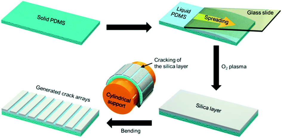 | ||
| Fig. 1 A schematic diagram of the fabrication steps for periodic crack patterns on the liquid-PDMS-covered elastomeric substrate formed by oxygen plasma and bending. | ||
After the oxygen plasma treatment, the PDMS substrate was wrapped around a cylindrical support and subsequently put on the glass slide. The wrapping step induces cracking on the stiff silica layer due to the tensile stress at the interface between the PDMS substrate and the native liquid PDMS caused by bending. Fig. S2c† shows the liquid PDMS exposed by cracking the silica layer due to bending. The microscope image in Fig. S2c† was taken from a thicker liquid PDMS sample to more easily observe the cracked regions with low-magnification optical microscopy. We could thereby produce periodic crack patterns on the elastomeric substrate consisting of a hardened silica layer and the exposed liquid PDMS along the cracks. The prepared crack-patterned PDMS substrate was used to synthesize gold NPs along these periodic crack arrays.
Patterned gold nanoparticle arrays were synthesized in situ on the cracked PDMS substrate in aqueous gold precursor solution. Fig. 2a shows a schematic illustration of the CTRL process to synthesize of gold NPs along the cracked line on the PDMS substrate. The intensity of the transmittance of the reddish color and the reflectance of the gold color both increased along with the reaction time, indicating that gold NPs were formed (Fig. 2b). The reduction of the gold ions to gold NPs was only observed in the exposed crack regions due to the presence of the PDMS curing agent. This curing agent consisted with Si–H groups, which could reduce the metal ions to metal particles (Fig. S3†).23–26 However, the silica layer on the liquid PDMS surface formed by oxygen plasma had low metal ion permeability. In addition, the Si–H group of the curing agent on the PDMS surface may have been be almost completely consumed during the oxygen plasma treatment.27 Therefore, the cracked regions gradually became red according to the formation of the gold nanoparticles, while the silica layer regions exhibited no color changes. Thus, aligned gold NP arrays were fabricated from the reduction lithography.
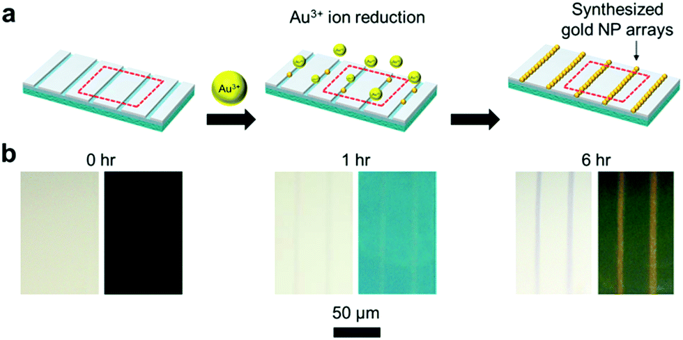 | ||
| Fig. 2 In situ synthesis of gold NPs along the cracked lines on the PDMS substrate. (a) A schematic illustration of the synthesis of gold NPs by crack templated reduction lithography (CTRL). (b) The transmittance (left) and reflection (right) optical images of the perpendicular crack lines at the same region during the 6 h reduction reaction. | ||
The morphologies of the synthesized gold NP arrays were examined by SEM and AFM. After finishing the reduction lithography, the patterned gold NP arrays were perpendicular to the direction of the applied external stress. In the SEM images, the aligned gold NP arrays appeared bright, while the regions covered with the silica layer were observed to be dark (Fig. 3a). SEM inset image shows the cross-sectional view of the synthesized gold NP array on PDMS substrate. Due to the large number of electrons in elements with a higher atomic number, the synthesized gold NP arrays appear significantly brighter than the PDMS substrate, which contains lower atomic-number elements. The presence of gold NPs at the cracked regions was also confirmed by EDS mapping (Fig. S4†). The results indicated that the gold NPs could be selectively synthesized at the regions defined by cracking on the PDMS substrate. Thus, the lines were composed of densely aligned gold NPs approximately 100 nm in diameter. The AFM analysis indicated that the width and amplitude of the gold NP arrays were approximately 800 nm and 120 nm, respectively (Fig. 3b). Thus, the AFM 3D line view of the geometry confirms that the wire-like 1D gold NP arrays were composed of densely connected individual gold NPs (Fig. 3c).
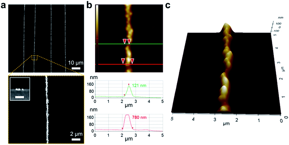 | ||
| Fig. 3 Morphological characteristics of the synthesized gold NP arrays. (a) FE-SEM image of the aligned gold nanoparticle composite wire arrays. Inset image shows the cross-sectional view and the scale bar is 1 μm. (b) AFM image of the gold NP array with a scan size of 5 × 5 μm. The inserted z-scale bar corresponds to 0 to 200 nm from bottom to top. (c) AFM 3D view of the produced gold NP array with a scan size of 5 × 5 μm. | ||
The gold NP arrays on the PDMS substrates were also examined by UV-visible spectroscopy. After the reduction lithography, a distinct peak at approximately 560 nm due to gold surface plasmon absorption appeared, while the bare PDMS exhibited no absorption peaks (Fig. 4). The absorption intensity increased at distinct wavelengths, indicating the formation of gold NPs on PDMS substrate. It is well known that the absorption peak of gold NPs is a function of the NPs diameter and as the diameter increases, the absorption shifts to longer wavelength due to the plasmon resonance and broaden due to the scattering with NPs size. From Fig. 4, the absorption peak at approximately 560 nm was related to 100 nm gold NPs and showed that the peak broaden like the previously reports.28–30 The size of the synthesized gold NPs along the cracked regions may be controlled by modulating the concentration of the metal precursor solution.31
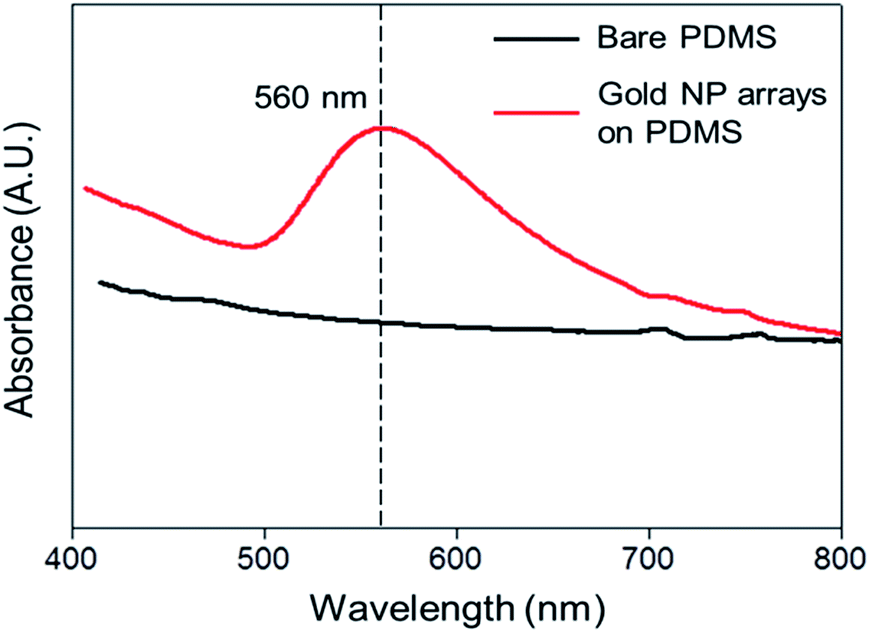 | ||
| Fig. 4 UV-visible spectra of a bare PDMS substrate and the gold NP arrays on PDMS. | ||
To control the periodicity between the 1D gold NP arrays, we used cylindrical supports with different diameters of 10, 15, and 30 mm. The cracked patterns on the PDMS substrate were fabricated by the same conditions described above. Then, the number of arrays in a 200 μm unit of length was counted in the optical microscope images (Fig. S5†). The evaluated numerical data demonstrated that more frequent arrays were fabricated by using a smaller diameter cylindrical support to induce the more cracking in the silica layer on the PDMS substrate. Approximately 40 arrays were fabricated in 200 μm in the case of the 10 mm diameter cylindrical support, while 18 and 2 arrays were observed for the 15 and 30 mm diameter cylindrical supports, respectively (Fig. S6†). The number of periodic arrays could be simply controlled by utilizing cylindrical supports with different diameters. Previous reports have demonstrated that cracked lines in PDMS could be easily modulated by gradual oxidation and the bending stress.32,33
Various patterned arrays were fabricated by applying step-wise stress with an orientation angle, a point stress, and by controlling the liquid PDMS thickness (Fig. 5). By applying single bending utilizing a cylindrical support, periodically aligned gold NP arrays were fabricated in the direction perpendicular to the tensile stress (Fig. 5a). A mesh-type wire pattern was prepared by applying bi-directional sequential bending with an orientation angle (Fig. 5b). The reflection image clearly shows the mesh-type wire pattern. Longer gold NP arrays formed by first bending and shorter gold NP arrays formed by second bending were observed by vertical incidence of light (shown as yellow arrow in Fig. 5b). A concentric wire pattern was obtained by applying high stress at a single point using a sharp tip (Fig. 5c). After the oxygen plasma treatment, the designated area was pressed with the tip, and reduction lithography was conducted to synthesize gold NPs in solution. Then, the concentrically aligned gold NP arrays were simply fabricated on the PDMS substrate. Finally, gold NP arrays consisting of wide and narrow regions were fabricated by spreading the liquid PDMS on the substrate using a rigid mold with a 5 μm height step (Fig. 5d). Through the oxygen plasma and bending process, wider cracks occurred in the PDMS regions with a thicker layer of liquid underneath, while narrow cracks were fabricated in surfaces covering the thinner liquid PDMS. The wider crack formation at the thicker liquid PDMS might be due to the higher fluid mobility of the un-cured PDMS depending on the thickness. The optical microscope image shows narrow and wide regions in a single wire. The various gold NP arrays were fabricated by the proposed simple CTRL method without using additional reducing/stabilizing agents or conventional MEMS processes.
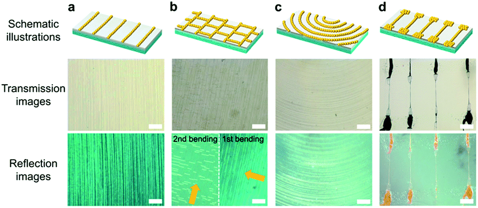 | ||
| Fig. 5 Fabrication of various gold NP array patterns by the CTRL method. (a) Transmission and reflection images of periodically aligned gold NP arrays. (b) The mesh-type wire pattern was produced by applying step-wise tensile stress with an orientation angle. (c) The concentric array pattern was obtained by pressing the designated region with a sharp tip. (d) Single array lines consisting of wide and narrow regions were fabricated using a hard mold with a 5 μm step. Scale bars are 100 μm in all optical microscope images. | ||
In summary, we have developed a novel CTRL method for the preparation of highly aligned gold NPs on an elastomeric PDMS substrate without additional reducing/stabilizing agents or MEMS processes. In the developed method, high reducing capacity regions were created by forming a silica layer on the surface of the liquid PDMS by oxygen plasma and inducing cracks in this layer using various bending processes. The exposed native liquid PDMS along the cracked lines was used as a template, wherein gold precursors were reduced by the curing agent of the PDMS. The resulting 1D gold NP arrays were well aligned along the direction of the cracks on the PDMS substrate and were generally homogeneous in width and height. This process also enabled the preparation of various patterns of gold NP arrays by applying step-wise stress with an orientation angle, a point stress, and by controlling the liquid PDMS thickness. We anticipate that our technique will be further optimized for optical and chemical sensing and for stretchable electronics.
Acknowledgements
This research was supported by Main Research Program (E0152203-03) of the Korea Food Research Institute (KFRI) funded by the Ministry of Science, ICT & Future Planning.Notes and references
- P.-C. Hsu, S. Wang, H. Wu, V. K. Narasimhan, D. Kong, H. R. Lee and Y. Cui, Nat. Commun., 2013, 4, 2522 CrossRef PubMed.
- G. Zheng, F. Patolsky, Y. Cui, W. U. Wang and C. M. Lieber, Nat. Biotechnol., 2005, 23, 1294–1301 CrossRef CAS PubMed.
- J. Kane, M. Inan and R. F. Saraf, ACS Nano, 2009, 4, 317–323 CrossRef PubMed.
- G. Peng, U. Tisch, O. Adams, M. Hakim, N. Shehada, Y. Y. Broza, S. Billan, R. Abdah-Bortnyak, A. Kuten and H. Haick, Nat. Nanotechnol., 2009, 4, 669–673 CrossRef CAS PubMed.
- A. De Ninno, G. Ciasca, A. Gerardino, E. Calandrini, M. Papi, M. De Spirito, A. Nucara, M. Ortolani, L. Businaro and L. Baldassarre, Phys. Chem. Chem. Phys., 2015, 17, 21337–21342 RSC.
- J. W. Jeong, S. R. Yang, Y. H. Hur, S. W. Kim, K. M. Baek, S. Yim, H.-I. Jang, J. H. Park, S. Y. Lee and C.-O. Park, Nat. Commun., 2014, 5, 5387 CrossRef CAS PubMed.
- P. Wang, L. Zhang, Y. Xia, L. Tong, X. Xu and Y. Ying, Nano Lett., 2012, 12, 3145–3150 CrossRef CAS PubMed.
- A. Kumar, H. A. Biebuyck and G. M. Whitesides, Langmuir, 1994, 10, 1498–1511 CrossRef CAS.
- V. M. Prida, J. García, L. Iglesias, V. Vega, D. Görlitz, K. Nielsch, E. D. Barriga-Castro, R. Mendoza-Reséndez, A. Ponce and C. Luna, Nanoscale Res. Lett., 2013, 8, 263 CrossRef PubMed.
- Y.-T. Hsieh and I. W. Sun, Chem. Commun., 2014, 50, 246–248 RSC.
- S. Xu, S. Joseph, H. Zhang, J. Lou and Y. Lu, RSC Adv., 2016, 6, 66484–66489 RSC.
- E. J. Menke, M. A. Thompson, C. Xiang, L. C. Yang and R. M. Penner, Nat. Mater., 2006, 5, 914–919 CrossRef CAS PubMed.
- F. Yang, D. K. Taggart and R. M. Penner, Nano Lett., 2009, 9, 2177–2182 CrossRef CAS PubMed.
- Y. S. Oh, D. Y. Choi and H. J. Sung, RSC Adv., 2015, 5, 64661–64668 RSC.
- P. Wünnemann, M. Noyong, K. Kreuels, R. Brüx, P. Gordiichuk, P. van Rijn, F. A. Plamper, U. Simon and A. Böker, Macromol. Rapid Commun., 2016, 37, 1446–1452 CrossRef PubMed.
- E. Mele, G. C. Anyfantis, D. Fragouli, R. Ruffilli and A. Athanassiou, RSC Adv., 2014, 4, 20449–20453 RSC.
- T. Zhang, W. Wang, D. Zhang, X. Zhang, Y. Ma, Y. Zhou and L. Qi, Adv. Funct. Mater., 2010, 20, 1152–1160 CrossRef CAS.
- H. J. Kim, Y. Roh and B. Hong, IEEE Trans. Nanotechnol., 2010, 9, 254–257 CrossRef.
- C. F. Monson and A. T. Woolley, Nano Lett., 2003, 3, 359–363 CrossRef CAS.
- X. Fu, Y. Wang, L. Huang, Y. Sha, L. Gui, L. Lai and Y. Tang, Adv. Mater., 2003, 15, 902–906 CrossRef CAS.
- S. Kurosawa, B.-G. Choi, J.-W. Park, H. Aizawa, K.-B. Shim and K. Yamamoto, Thin Solid Films, 2006, 506, 176–179 CrossRef.
- T. Kashiwagi, K. Okabe and K. Okita, J. Membr. Sci., 1988, 36, 353–362 CrossRef CAS.
- I. Choi, Y. Shin, J. Song, S. Hong, Y. Park, D. Kim, T. Kang and L. P. Lee, ACS Nano, 2016, 10, 7639–7645 CrossRef CAS PubMed.
- A. Goyal, A. Kumar, P. K. Patra, S. Mahendra, S. Tabatabaei, P. J. J. Alvarez, G. John and P. M. Ajayan, Macromol. Rapid Commun., 2009, 30, 1116–1122 CrossRef CAS PubMed.
- J. Sun, J. Jiang, B. Bao, S. Wang, M. He, X. Zhang and Y. Song, Materials, 2016, 9, 253 CrossRef.
- R. Gupta, H. K. Nagamanasa, R. Ganapathy and G. U. Kulkarni, Bull. Mater. Sci., 2015, 38, 817–823 CrossRef CAS.
- Q. Zhang, J.-J. Xu, Y. Liu and H.-Y. Chen, Lab Chip, 2008, 8, 352–357 RSC.
- M. Honda, Y. Saito, N. I. Smith, K. Fujita and S. Kawata, Opt. Express, 2011, 19, 12375–12383 CrossRef CAS PubMed.
- P. K. Jain, K. S. Lee, I. H. El-Sayed and M. A. El-Sayed, J. Phys. Chem. B, 2006, 110, 7238 CrossRef CAS PubMed.
- N. G. Bastús, J. Comenge and V. Puntes, Langmuir, 2011, 27, 11098 CrossRef PubMed.
- M.-C. Daniel and D. Astruc, Chem. Rev., 2004, 104, 293–346 CrossRef CAS PubMed.
- H.-N. Kim, S.-H. Lee and K.-Y. Suh, Lab Chip, 2011, 11, 717–722 RSC.
- M. Melzer, G. Lin, D. Makarov and O. G. Schmidt, Adv. Mater., 2012, 24, 6468–6472 CrossRef CAS PubMed.
Footnote |
| † Electronic supplementary information (ESI) available: Materials and methods, fabrication of crack patterns on PDMS substrate, in situ synthesis of the gold NPs in cracked regions, characterization; additional microscopic analysis and elemental mapping of gold NP arrays, characteristics of produced silica layer by plasma treatment, schematic illustration of gold NP formation mechanism, and periodicity of produced gold NP arrays. See DOI: 10.1039/c7ra00768j |
| This journal is © The Royal Society of Chemistry 2017 |