 Open Access Article
Effect of copper oxide shell thickness on flash light sintering of copper nanoparticle ink†
Gyung-Hwan Oha,
Hyun-Jun Hwanga and
Hak-Sung Kim *ab
*ab
aDepartment of Mechanical Convergence Engineering, Hanyang University, Haengdang-dong, Seongdong-gu, Seoul 166-791, South Korea. E-mail: kima@hanyang.ac.kr; Fax: +82-2220-2299; Tel: +82-2-2220-2898
bInstitute of Nano Science and Technology, Hanyang University, Seoul, 133-791, Korea
First published on 22nd March 2017
Abstract
In this study, the effect of the thickness of a copper oxide-shell on flash light sintering of Cu nanoparticles (NPs) was investigated. The electrical properties of Cu nano-ink films with various oxide-shell thicknesses were examined by measuring the sheet resistance. Furthermore, the amount of PVP in the Cu NP-ink was varied to reduce the copper oxide-shell efficiently and enhance the flash light sintering of the Cu NPs. Also, to investigate the reduction and sintering phenomena of Cu NPs with respect to the copper oxide shell thickness, the sheet resistances of the Cu films were measured in real-time using an in situ resistance measuring system during the flash light sintering process. The results of this study established the maximum allowable thickness of the copper oxide shell that allows flash light sintering and also provided the optimal amount of PVP in Cu nano-ink for a particular copper oxide shell thickness.
1. Introduction
Recently, printed electronics have received increased attention as an alternative manufacturing process for electronic devices such as radio frequency identification (RFID) tags, wearable electronics, and solar cells1,2 because of their rapid and low-cost processing compared to the conventional photolithographic processes.3 The core technologies for printed electronics, including nanomaterial-based conductive inks, printing technologies, and sintering processes, have been developed and are being actively studied.Conventionally, nanomaterial-based conductive inks made with noble metals (such as Au and Ag) have been used in printed electronics because of their excellent conductivity, stability, and sintering efficiency under conventional processing conditions. However, these noble metals are not suitable for mass-production due to their high cost. For this reason, copper nanoparticle inks have received much attention as a low-cost substitute for silver or gold nanoparticles inks.4 However, copper nanoparticles (NPs) are easily oxidized in air, which results in a decrease in the electrical conductivity of Cu films. Thus, reduction of the oxide shell on the surface of the Cu NPs during sintering is necessary for obtaining highly conductive Cu films. It was also necessary to sinter Cu NPs at low temperature because Cu NPs are easily oxidized at high temperature under ambient conditions. Laser5–7 and microwave8,9 sintering methods have been studied to solve these problems. However, these methods have limitations in mass-production because of their complexity and environmental restrictions (e.g., vacuum pressures). Moreover, they are not suitable for sintering large areas. Therefore, a new sintering technique enabling low temperature and rapid large area sintering is needed for the commercialization of flexible printed electronic devices.
We previously developed a flash light sintering process combined with PVP functionalized Cu NP-inks to overcome the limitations mentioned above.10–12 Flash light sintering can reduce the copper oxide shell and sinter copper nanoparticles at room temperature under ambient conditions in just a few milliseconds without damaging the substrate. In addition, a flash light from a xenon lamp allows sintering of a large area. However, an in-depth study of the effect of copper oxide shell thickness on the flash light sintering of the Cu NP-ink has not yet been conducted.
Therefore, we investigated the effect of copper oxide shell thickness on the flash light sintering of Cu NPs in this study. Cu NPs covered with copper oxide shells that were 0.8 nm to 14 nm in thickness were prepared by heating to 25–500 °C in air. The prepared Cu NPs were sintered by flash light irradiation with various energy densities from 7.5 J cm−2 to 12.5 J cm−2. The amount of PVP in the Cu NP-ink was optimized with respect to the thickness of the oxide shell to enhance the reduction and sintering of the Cu NPs with a thick oxide shell. Furthermore, the number of pulse flashes was varied to efficiently reduce thick copper oxide shells without rapid volume contraction.
The thickness of the copper oxide-shell was measured using transmission electron microscopy (TEM), and the microstructures of the sintered Cu film were observed using scanning electron microscopy (SEM). Crystal phase analysis using X-ray diffraction (XRD) was performed to study the chemical shift of the copper nanoparticles. The sheet resistances of the Cu film were measured in real-time using an in-house resistance measurement system to investigate the reduction and sintering phenomena of the copper nanoparticles with respect to the copper oxide shell thickness.
2. Materials and methods
2.1 Specimen preparation
Commercially available Cu nanoparticles with an oxide shell (20–50 nm in diameter, copper(II) oxide shell; QSI-nano) were used in this study. Cu NPs with various oxide shells were prepared by heating at different temperatures using a forced convection oven for 2 hours (Table 1). To oxidize copper nanoparticles uniformly, Cu NPs were evenly spread on a plate. The prepared Cu NPs (11.4 g) were dispersed in a mixed solvent of diethylene glycol (DEG, 99%; Samchun Chemical) (6 g) and poly(N-vinylpyrrolidone) (PVP, MW 40![[thin space (1/6-em)]](https://www.rsc.org/images/entities/char_2009.gif) 000; Sigma Aldrich) (0.9–1.0 g) using a three-roll mill. The amount of PVP was fixed at 0.9 g in order to observe how sintering changes with the thickness of the copper oxide shell. The amount of PVP was varied from 0.9 to 1.0 g with intervals of 0.025 g to optimize PVP content in the flash light sintering process. The fabricated Cu NP-inks were printed on a polyimide (PI) substrate using a doctor blade method and were dried on a hot plate (100 °C) for 3 h.
000; Sigma Aldrich) (0.9–1.0 g) using a three-roll mill. The amount of PVP was fixed at 0.9 g in order to observe how sintering changes with the thickness of the copper oxide shell. The amount of PVP was varied from 0.9 to 1.0 g with intervals of 0.025 g to optimize PVP content in the flash light sintering process. The fabricated Cu NP-inks were printed on a polyimide (PI) substrate using a doctor blade method and were dried on a hot plate (100 °C) for 3 h.
| Acronym of copper nanoparticles | Heating temperature (during 2 hours) | Thickness of copper oxide shell |
|---|---|---|
| Cu NPs-RT | 25 °C | 0.8 nm |
| Cu NPs-100 | 100 °C | 2.1 nm |
| Cu NPs-200 | 200 °C | 3.6 nm |
| Cu NPs-300 | 300 °C | 7.1 nm |
| Cu NPs-400 | 400 °C | 12.6 nm |
| Cu NPs-500 | 500 °C | 14.0 nm |
2.2 Flash light sintering and in situ monitoring of Cu NP-ink
The printed Cu NP-inks were sintered by flash light irradiation at room temperature and ambient conditions. The flash light sintering system consisted of a xenon lamp (Perkin-Elmer Co,), a power supply (PSTek Co.), capacitors, a pulse controller, and a reflector (Semisysco Co) (Fig. 1). The white light from the xenon lamp has a broad wavelength range from 380 to 950 nm. Cu NP-ink films were placed at a distance of 3 mm from the lamp and the irradiation energy was varied from 7.5 J cm−2 to 12.5 J cm−2. In order to observe the thickness effect of the copper oxide shell, the number of pulses, on-time, and off-time were fixed at the optimized values from the previous study results.13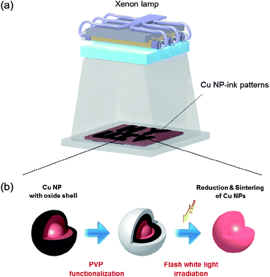 | ||
| Fig. 1 Schematics of the photonic sintering process of Cu NP-ink with copper oxide shell using flash white light. | ||
In order to monitor the sintering process in real time, the change in the resistance of the Cu NP-ink films over a period of a few milliseconds was measured using a Wheatstone bridge electrical circuit, a source meter (2611A; Keithley), and an oscilloscope (DL1740E; Yokogawa).
2.3 Characterization
The thickness of the copper oxide-shell was measured using transmission electron microscopy (TEM, JEM-2100F) and the microstructures and surfaces of the sintered Cu film were observed using scanning electron microscopy (SEM, S4800 Hitachi). Crystal phase analysis was performed using X-ray diffractometry (XRD, D/MAX RINT 2000, Cu Kα radiation) to investigate the oxidation or reduction of the oxide. The electrical sheet resistances of the Cu nanofilms were measured using a four-point probe method.3. Results and discussion
HR-TEM was used to evaluate the oxide shells of the Cu nanoparticles (NPs). Cu NPs used in this study were manufactured using a vapor condensation process, which resulted in a copper(II) oxide (CuO) shell on the surface of the nanoparticles for passivation.14,15 For this reason, a copper oxide shell that was 0.8 nm thickness was observed even for the non-treated copper nanoparticles (Fig. 2a). It was also observed that the thickness of the copper oxide shell increased from 2.1 nm to 14 nm as the oxidation temperature increased from 100 °C to 500 °C (Fig. 2b–f) and these values were determined through averaging that based on various TEM images (Fig. S1a–f†). This is because Cu nanoparticles were easily oxidized in the air, and high temperature accelerated the oxidation.16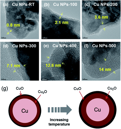 | ||
| Fig. 2 HR-TEM images of (a) Cu NPs-RT, (b) Cu NPs-100, (c) Cu NPs-200, (d) Cu NPs-300, (e) Cu NPs-400, (f) Cu NPs-500 and (g) schematic illustration of the surface composition change of Cu NPs. | ||
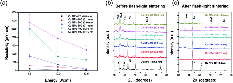
XRD patterns shown in Fig. 3b demonstrated that pure copper phase peaks (43.2°, 50.4° and 74.1°) decreased and copper(I) oxide (Cu2O) peaks (36.4° and 38°) increased as the oxidation temperature increased.17 This means that higher temperature caused significant oxidation of pure copper in air as shown in eqn (1), which produces a thicker copper oxide shell (Cu2O). When the temperature was higher than 300 °C, the peaks associated with copper(II) oxide (35.5° and 38.7°) remarkably increased and pure Cu phase peaks (43.2°, 50.4° and 74.1°) were difficult to observe because the copper(I) oxide shell on the surface of the Cu NPs was further oxidized eqn (2), resulting in thick Cu oxide shells.
| 4Cu + O2 → 2Cu2O | (1) |
| 2Cu2O + O2 → 4CuO | (2) |
Key data from the characterization of Cu NPs are schematically illustrated in Fig. 2g. Cu NPs were oxidized under ambient atmospheric conditions to form a surface oxide composed of Cu2O (detected by FTIR and XRD), which was covered with a thin outer layer of CuO (XPS, XRD, and FTIR).18 The temperature of the atmosphere played a significant role. Specifically, a Cu2O layer was formed on the surface of the Cu NPs below 100 °C, while a complex oxide of Cu3O2 formed at about 150 °C. A thin layer of CuO formed on the outer layer at temperatures above 200 °C. Thus, the compounds observed during formation of a Cu oxide shell (CuxO) followed the order Cu2O, Cu3O2, and CuO with increasing temperature; eventually, all oxides coexisted on the surface.19–21 The results of XRD (Fig. 3b) are in agreement with these results from previous studies. The copper(II) oxide (CuO) peaks were observed even in the non-heated Cu nanoparticles (Cu NPs-RT) (see the black line in Fig. 3b), and these were derived from the synthesis process of Cu NPs.
To reduce and sinter the Cu NPs with a copper oxide shell, we functionalized the Cu NPs with PVP (Cu NPs: 11.4 g, PVP: 0.9 g) and varied the irradiation energy of the flash light from 7.5 J cm−2 to 12.5 J cm−2; one pulse of flash light with a duration of 10 ms was used, based on our previous study.13 As shown in Fig. 3a, the resistivity of the Cu NP-ink films decreased as the irradiation energy increased up to 12.5 J cm−2. These results are consistent with those reported in our previous studies.13 The PVP layer decomposed and evaporated after flash light irradiation, allowing the copper oxide shell to be reduced. The copper nanoparticles were simultaneously sintered by the flash light, resulting in a decrease in resistivity. However, it was found that Cu NPs with thicker oxide shells had a higher resistivity after flash light sintering (Fig. 3a). This may be because Cu oxide shells disturbed the sintering of Cu NPs during flash light irradiation. XRD patterns shown in Fig. 3c demonstrated that pure copper phase peaks (43.2°, 50.4° and 74.1°) decreased as the thickness of the oxide shell increased, although the intensity of the pure Cu phase peaks increased and the peaks of the Cu oxide (CuO and Cu2O) decreased after flash light irradiation. Therefore, it could be concluded that the copper oxide shell disturbs the sintering of the Cu NPs. The peaks associated with copper(II) oxide (CuO) were entirely removed for all cases after flash light sintering (Fig. 3c). This indicates that copper(II) oxide (CuO) was reduced to pure copper by OH radicals derived from PVP decomposition through flash light irradiation according to eqn (3).22,23
| CuO + 2OH → Cu + H2O + O2 | (3) |
| 2CuO + 2OH → Cu2O + H2O + O2 | (4) |
However, when the oxidation temperature was higher than 300 °C, peaks associated with copper(I) oxide (Cu2O) remained even after flash light sintering. Thus, Cu oxide shells thicker than 7.1 nm (>300 °C) were not reduced fully due to a lack of OH radicals from PVP chains, resulting in residual copper(I) oxide (Cu2O) eqn (4). Moreover, the thick oxide shell caused agglomeration in Cu NPs as shown in Fig. S2a–c† because hydrophilic copper oxide enhanced the agglomeration of NPs due to their highly polar nature.24,25 The agglomeration of NPs reduced the surface area for PVP adhesion, resulting in an incomplete reduction of Cu oxide and a low uniformity in the Cu NP-ink films (Fig. S2d†). For these reasons, the resistivity of the sintered Cu NPs-300, 400 and 500 with oxide shells thicker than 7.1 nm (>300 °C) dramatically increased (Fig. 3a).
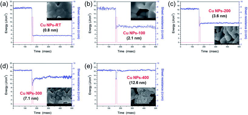
In order to investigate the reduction of the oxide shell and flash light sintering mechanism of Cu NPs, a Wheatstone bridge electrical circuit and an oscilloscope were used to monitor the sintering process of Cu NP-ink (PVP weigh fraction: 7.3%) in real time under optimum irradiation energy conditions (irradiation energy of 12.5 J cm−2, pulse number of 1, pulse duration of 10 ms) (Fig. 4). It was observed that the electrical resistance of the Cu NPs-1 ink film decreased to about 3.7 Ω sq−1 immediately after flash light irradiation (Fig. 4a). In this period, the Cu oxide shell surrounding the Cu NPs might be reduced via decomposition of the PVP coating layer and sintered by flash light irradiation. However, we found that the decrease in the resistance during flash light irradiation was restricted as the oxidation temperature increased (Fig. 4b–e). Moreover, when the Cu oxide shell was thicker than 2.1 nm, the sheet resistance increased again during flash light irradiation. This may be because the Cu oxide was not reduced fully and Cu NPs were re-oxidized during flash light irradiation due to a lack of PVP chains, resulting in more inter-granular pores as shown in the SEM images (see insets in Fig. 4b–e). Also, when the oxidation temperature was higher than 400 °C, the sintered Cu NP films had an island-like film surface (Fig. 4e) because of the agglomeration of Cu NPs with a thick oxide shell. These results corresponded to the previous electrical resistivity and XRD results (Fig. 3). Hwang et al. demonstrated that the PVP amount for a complete reduction of copper oxide is linearly proportional to the amount of copper oxide shell.13 Therefore, it was necessary to optimize the amount of PVP with respect to the thickness of the Cu oxide shell to enhance the reduction of the Cu oxide shell and improve the electrical resistivity.
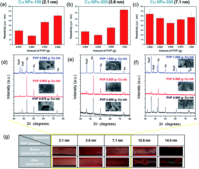
The optimal amount of PVP in Cu NP-RT ink was previously determined to be 7.3 wt% (0.9 g PVP and 11.4 g Cu NPs) to ensure the full-reduction of a thin Cu oxide shell (thickness of 0.8 nm).13 To fully reduce thick Cu oxide shells, the amount of PVP was increased to 1.0 g. As shown in Fig. 5a–c, inks of Cu NPs-100, 200 and 300 showed the lowest electrical resistivity when the amount of PVP was 0.900 g, 0.925 g, and 0.950 g, respectively. As shown in the XRD patterns, we also observed that the copper(II) oxide (CuO) phase peaks (35.5° and 38.7°) disappeared completely and copper(I) oxide (Cu2O) phase peaks (36.4°) decreased, while pure Cu phase peaks (43.2°, 50.4°, and 74.1°) increased after the optimization of PVP amount (Fig. 5d–f). This is because the amount of PVP was sufficient to efficiently reduce the Cu oxide shells, resulting in a lower porosity and more connections among the nanoparticles compared to cases with less PVP and the worst resistivity (see inset SEM images in Fig. 5d–f). Optimization of the amount of PVP with respect to the thickness of the oxide shell resulted in an enhanced reduction of Cu oxide and improved sintering of Cu NPs, which reduced the electrical resistivity of the sintered Cu films. However, when the Cu oxide shell thickness was 7.1 nm, the resistivity of the sintered Cu film was still high (about 450 μΩ cm) even after the amount of PVP was optimized. Moreover, when the Cu oxide shell thickness was thicker than 12.6 nm, more PVP functionalization caused damage in the Cu films after flash light irradiation, as shown in Fig. 5g. Thicker layers of PVP and Cu oxide shells disrupted the light absorption and the sintering of Cu NPs and caused delamination of Cu films due to the residual layers of PVP and Cu oxide on the Cu NPs. Therefore, it was concluded that Cu NPs with oxide shells thicker than 10 nm were not suitable for the flash light sintering process. Cu NPs with oxide shells less than 7 nm thick were necessary for fabricating highly conductive Cu NP-inks.
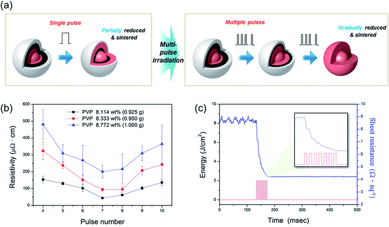
It was also found that the Cu NP-200 ink still had a high resistivity (Fig. 5b), and the copper(I) oxide (Cu2O) phase peak (36.4°) still remained in this sample even after optimization of the amount of PVP (Fig. 5e). This may because the PVP layers were not decomposed entirely by flash light with a single pulse because they were quite heavy. Incomplete decomposition of PVP resulted in an incomplete reduction of the Cu oxide shell (Fig. 6a). To resolve these problems, multiple pulses (irradiation energy per pulse of 2 J cm−2, pulse duration of 3 ms, and pulse gap of 3 ms) were applied with an increasing number of pulses from 4 to 10. It was noteworthy that the resistivity of the Cu films decreased as the pulse number increased up to 7 (Fig. 6b). This was because a thick Cu oxide shell was gradually reduced with PVP decomposition, and Cu NPs were increasingly sintered as the number of pulses increased (Fig. 6a). To investigate the gradual reduction and sintering process, the sheet resistance change observed in a Cu film was monitored during multi-pulsed flash light irradiation in real time (Fig. 6c). The sheet resistance of the Cu films decreased incrementally after each flash light pulse irradiation. The sheet resistance decreased significantly after the first and the second pulses, followed by less significant decreases after the following pulses. Finally, the sheet resistance stabilized at its final value (4.2 Ω sq−1) after the seventh pulse. Both the reduction of the Cu oxide shell and sintering of Cu NPs continued during pulse irradiation up to the seventh pulse. However, the resistivity increased again when more than 7 pulses were used because Cu NPs were re-oxidized due to the excessive irradiation energy (Fig. 6b). We also found that 0.925 g of PVP produced a higher conductivity than any other PVP amount (Fig. 6b), which was in agreement with the results of the PVP optimization (Fig. 5).
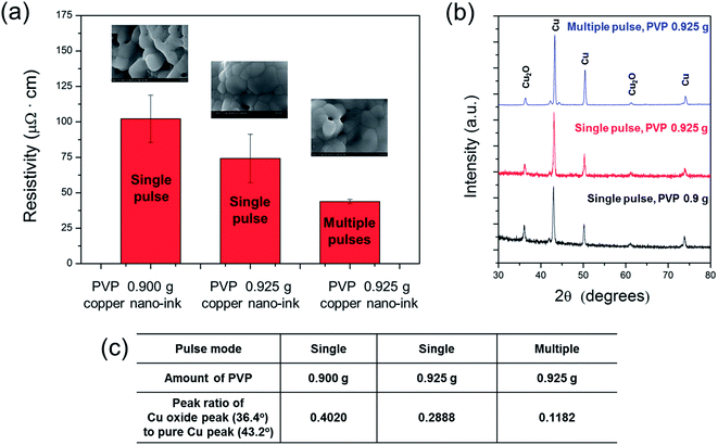
Fig. 7a shows a comparison of the resistivity of the Cu NP-200 (3.6 nm thick oxide shell) films sintered by flash light. As shown, the Cu NP-200 ink functionalized by 0.925 g of PVP had smaller pore sizes and more connections among the nanoparticles than those of the 0.900 g PVP case, which resulted in a decrease in the electrical resistivity (−27.6%). This was because the higher amount of PVP more effectively reduced the thick Cu oxide shells. Meanwhile, the lowest resistivity Cu film was obtained using multiple flash light irradiations. The XRD pattern of the optimal PVP functionalized (PVP of 0.925 g) and sintered (pulse number of 7, irradiation energy per pulse of 2 J cm−2, 3 ms pulse duration, and 3 ms pulse gap) Cu NP-200 ink showed a pure Cu peak (43.2°) with less Cu oxide (36.4°) due to further reduction of the Cu oxide shells and crystallization of the pure Cu phase (Fig. 7b) and the peak ratios of Cu oxide peak (36.4°) to pure Cu peak (43.2°) were 0.4020, 0.2888 and 0.1182 in cases of single pulse with 0.900 g PVP, single pulse with 0.925 g PVP and multiple pulse with 0.925 g, respectively (Fig. 7c). Furthermore, as shown in the inset SEM image in Fig. 7a, the optimized conductive Cu film had a larger grain size and a resistivity of 43.83 μΩ cm, which was 57.1% lower than that obtained from a single pulse with 0.900 g PVP. Therefore, it was demonstrated that multi-pulsed flash light irradiation enhanced the reduction and sintering of Cu NPs with thick Cu oxide shells and PVP layers.
Multiple pulses reduced and sintered the thick Cu oxide shell more effectively without an abrupt volume contraction as compared to single pulse processes. Unfortunately, however, the resistivity of the optimally sintered Cu film with a 3.6 nm thick oxide shell (43.83 μΩ cm) was still higher than that of the Cu film with a 0.8 nm thick oxide shell (17.34 μΩ cm). This is due to the thick Cu oxide shell on the surface of the Cu NPs, which inhibits light absorption and sintering of Cu NPs. Even though the resistivity of the Cu film was still high, it is a highly significant discovery that Cu NPs with thick oxide shells (<7 nm) can be sintered by flash light irradiation at room temperature under ambient conditions in just a few milliseconds without damaging the substrate.
4. Conclusion
In this work, the effect of the thickness of the copper oxide shell on the flash light sintering of Cu NPs was investigated. In addition, the amount of PVP functionalization was optimized with respect to the thickness of the copper oxide shell in order to enhance the reduction and sintering of Cu NPs with a thick oxide shell. It was found that PVP functionalization improved the reduction of thick Cu oxide shells. However, Cu NPs with oxide shells thicker than 7 nm were not suitable for the flash light sintering method, because they agglomerated and showed a low reduction rate even after optimization of the amount of PVP. Therefore, it was concluded that it is preferable to have a copper oxide shell that is less than 4 nm thick for the flash light sintering process. It was also noteworthy that multi-pulsed flash light irradiations could decompose thick PVP layers and reduce thicker Cu oxide shells effectively without damaging the Cu films. The optimally PVP functionalized and flash light sintered Cu film with a 3.6 nm oxide shell had a resistivity of 43.83 μΩ cm, which was 57.1% lower than that of the non-optimized Cu film (102.2 μΩ cm). The novel photonic sintering technique for Cu NP-ink described here is a viable approach to realize room temperature in situ sintering of printed electronics.Acknowledgements
This work was supported by a National Research Foundation of Korea (NRF), funded by the Ministry of Education (2015R1D1A1A09058418, 2012R1A6A1029029) and grant funded by the Korean Government (MEST) (2013M2A2A9043280). This work was also supported by the Technology Innovation Program (or Industrial Strategic Technology Development Program, 10048913, Development of the cheap nanoink, which is sintered in the air for smart devices) funded by the Ministry of Trade, Industry, & Energy (MI, Korea).References
- J. Perelaer, A. W. De Laat, C. E. Hendriks and U. S. Schubert, J. Mater. Chem., 2008, 18, 3209–3215 RSC.
- S. K. Volkman, Y. Pei, D. Redinger, S. Yin and V. Subramanian, MRS Online Proc. Libr., 2004, 814 DOI:10.1557/PROC-814-I7.8.
- Z. Liu, Y. Su and K. Varahramyan, Thin Solid Films, 2005, 478, 275–279 CrossRef CAS.
- D. Li, D. Sutton, A. Burgess, D. Graham and P. D. Calvert, J. Mater. Chem., 2009, 19, 3719–3724 RSC.
- A. Simchi, Mater. Sci. Eng., 2006, 428, 148–158 CrossRef.
- M. Zenou, O. Ermak, A. Saar and Z. Kotler, J. Phys. D: Appl. Phys., 2013, 47, 025501 CrossRef.
- H. Zhu, L. Lu and J. Fuh, J. Mater. Process. Technol., 2003, 140, 314–317 CrossRef CAS.
- D. Demirskyi, D. Agrawal and A. Ragulya, Mater. Lett., 2010, 64, 1433–1436 CrossRef CAS.
- C.-L. Huang, R.-J. Lin and J.-F. Tzeng, Mater. Chem. Phys., 2006, 97, 256–260 CrossRef CAS.
- Y.-T. Hwang, W.-H. Chung, Y.-R. Jang and H.-S. Kim, ACS Appl. Mater. Interfaces, 2016, 8, 8591–8599 CAS.
- S.-J. Joo, H.-J. Hwang and H.-S. Kim, Nanotechnology, 2014, 25, 265601 CrossRef PubMed.
- H.-S. Kim, S. R. Dhage, D.-E. Shim and H. T. Hahn, Appl. Phys. A: Mater. Sci. Process., 2009, 97, 791–798 CrossRef CAS.
- H.-J. Hwang, W.-H. Chung and H.-S. Kim, Nanotechnology, 2012, 23, 485205 CrossRef PubMed.
- A. G. Nasibulin, P. P. Ahonen, O. Richard, E. I. Kauppinen and I. S. Altman, J. Nanopart. Res., 2001, 3, 383–398 CrossRef.
- A. G. Nasibulin, E. I. Kauppinen, D. P. Brown and J. K. Jokiniemi, J. Phys. Chem. B, 2001, 105, 11067–11075 CrossRef CAS.
- G. Raynaud and R. Rapp, Oxid. Met., 1984, 21, 89–102 CrossRef CAS.
- R. Wijesundera, Semicond. Sci. Technol., 2010, 25, 045015 CrossRef.
- K. Midander, P. Cronholm, H. L. Karlsson, K. Elihn, L. Möller, C. Leygraf and I. O. Wallinder, Small, 2009, 5, 389–399 CrossRef CAS PubMed.
- J.-H. Park and K. Natesan, Oxid. Met., 1993, 39, 411–435 CrossRef CAS.
- Y. Sawada, H. Tamaru, M. Kogoma, M. Kawase and K. Hashimoto, J. Phys. D: Appl. Phys., 1996, 29, 2539 CrossRef CAS.
- H. Wieder and A. Czanderna, J. Phys. Chem., 1962, 66, 816–821 CrossRef CAS.
- H.-J. Hwang, K.-H. Oh and H.-S. Kim, Sci. Rep., 2016, 6, 19696 CrossRef CAS PubMed.
- J. Ryu, H.-S. Kim and H. T. Hahn, J. Electron. Mater., 2011, 40, 42–50 CrossRef CAS.
- K. Barick, M. Aslam, V. P. Dravid and D. Bahadur, J. Phys. Chem. C, 2008, 112, 15163–15170 CAS.
- T. H. Tran and V. T. Nguyen, Int. Scholarly Res. Not., 2014, 2014, 14 Search PubMed.
Footnote |
| † Electronic supplementary information (ESI) available. See DOI: 10.1039/c7ra01429e |
| This journal is © The Royal Society of Chemistry 2017 |

