
 Open Access Article
 This Open Access Article is licensed under a Creative Commons Attribution-Non Commercial 3.0 Unported Licence
Improvement of the structural and electronic properties of CZTSSe solar cells from spray pyrolysis by a CuGe seed layer
M. H. Sayed *,
J. Schoneberg,
J. Parisi and
L. Gütay
*,
J. Schoneberg,
J. Parisi and
L. Gütay
Laboratory for Chalcogenide Photovoltaics, Department of Energy and Semiconductor Research, Institute of Physics, University of Oldenburg, 26111 Oldenburg, Germany. E-mail: mohamed.mohamed@uni-oldenburg.de
First published on 7th April 2017
Abstract
We have produced CZTSSe solar cells by a sequential growth process. First, CZTS precursors were deposited on Mo-coated soda lime glass substrates by chemical spray pyrolysis from an aqueous solution containing Cu, Zn and Sn metal salts and thiourea. In a second step the precursor was selenized at 530 °C for 8 min, resulting in fair solar cell properties. Further, we have investigated the influence of a 20 nm CuGe seed layer, which was sputtered on the Mo-surface prior to CZTS precursor deposition, on the morphology of the resulting absorber and on the performance of CZTSSe solar cells. We observe that the formation of MoSe2 and the consequent decomposition reactions at the back contact region of the CZTSSe layers during the annealing process were suppressed by introducing the CuGe seed layer, and that grain growth at the Mo/CZTSSe interface region was enhanced. The performance of CZTSSe solar cells prepared with a 20 nm CuGe seed layer shows considerable improvement compared to the processing without CuGe introduction.
Introduction
The kesterite compound Cu2ZnSn(S,Se)4 (CZTSSe) is a promising candidate for low-cost, less toxic and scalable thin film solar cells.1,2 Up to now, the highest achieved CZTSSe solar cell efficiency of 12.7% (ref. 3) is still far from the expected values of the theoretical calculations.4 A full comprehension of the CZTSSe processing and complete control of the fabrication process and the involved reactions are still required in order to obtain high efficiency CZTSSe solar cells.Various deposition techniques including vacuum5,6 and non-vacuum7,8 deposition methods have been reported in the literature for kesterite based solar cells. Mostly, the kesterite layers are processed via a two step fabrication process, including a precursor deposition step followed by a high temperature annealing process under a chalcogen atmosphere. A high chalcogen pressure during the annealing process is needed to suppress decomposition reactions of kesterite that can occur at high temperatures.9
The instability of the interface between the kesterite absorber and molybdenum (Mo) back contact is one of the main issues during the annealing process at high temperature, leading to formation of MoS(e)2 and resulting decomposition reactions.10 This may be one of the reasons for the comparably low performance of kesterite solar cells.11
Optimization of the kesterite/back contact interface and suppressing the formation of MoS(e)2 and other secondary phases during the annealing process might pave the way for achieving high efficient kesterite solar cells.
Introducing an intermediate barrier layer between the kesterite and Mo back contact is one of the strategies which have been reported to hinder the decomposition of kesterite at the Mo back contact. TiN has been demonstrated to inhibit the MoS(e)2 formation and hence decomposition reactions of CZTSSe at the back contact.12,13 However, TiN was found to induce high series resistance in the device12 and influence the crystallization of the absorber layer.13 Schnabel et al. introduced Mo/TiN/Mo sandwich structure to limit the thickness of the resulting MoSe2 layer above the TiN barrier and retain the large grain layer near the back contact.
Further, TiB2 intermediate layers have been reported to significantly inhibit the formation of MoS2 and accordingly reduce the series resistance and increase the device efficiency significantly, however introducing TiB2 layer degrades the CZTS absorber's crystallinity, leading to some degradation on device performance.14
ZnO also has been proposed to prevent the direct contact between Mo and kesterite and inhibits the decomposition reactions and showed an improvement in the device characteristics and a significant decrease in the device series resistance due to the improved absorber/back contact interface.15
Silver (Ag),16 carbon (C)17 and bismuth (Bi)18 elemental layers have also been investigated as probable candidates for back contact modification and showed, to some extent, an enhancement in the absorber quality and some properties of solar cell devices. However, besides their role as back contact modifications these elements may diffuse into the absorber during the annealing process and lead to additional effects on the device properties.
In this study, we introduce a CuGe seed layer as a feasible alternative back contact modification to (i) suppress the MoSe2 formation reaction during the annealing process and (ii) to act as a possible source for germanium (Ge) incorporation into the absorber layer during the annealing process.
Kesterite alloying with Ge has been intensively investigated in the last few years and showed beneficial effects on the quality of the kesterite absorber and the device performance.19–22 Tin (Sn) substitution with Ge allows for band gap tuning.23,24 In addition Ge incorporation decreases the tendency to form Sn2+ oxidation state, instead of SnIV+, which leads to the formation of detrimental deep levels recombination centers and carrier traps, thus limit the device efficiency.25
Giraldo et al.26 and Neuschitzer et al.22 showed a strong beneficial impact of Ge doping, using thin layers of thermally evaporated Ge on top of the precursor before annealing, on crystal growth and further solar cell device performance, especially the open circuit voltage.
In this paper, a CuGe seed layer is introduced at the Mo/CZTS interface and its impact on the MoSe2 formation during the annealing process and on the quality of CZTSSe absorbers is investigated. Furthermore, a correlation between the CZTSSe absorbers and the respective devices performance of CZTSSe thin film solar cells is reported.
Experimental
CuGe layers with a thickness of 20 nm were deposited on the Mo-coated soda lime glass (SLG) substrates by DC magnetron sputtering (Von-Ardenne CS400 cluster system) from a 100 mm diameter Cu66Ge34 target. The flow rate of argon (Ar) was kept at a constant value of 40 sccm. The sputtering pressure was 0.5 Pa and DC power was 50 W.CZTS precursors were deposited onto the SLG/Mo substrates with and without CuGe layer by chemical spray pyrolysis method. The precursor solution was prepared with 5.7 mmol copper nitrate trihydrate (Cu(NO3)2·3H2O, Sigma Aldrich), 4.3 mmol zinc nitrate hexahydrate (Zn(NO3)2·6H2O, Sigma Aldrich), 3.7 mmol tin methanesulfonate (Sn(CH3SO3)2, Sigma Aldrich) and 40 mmol thiourea (SC(NH2)2, Sigma Aldrich), which were dissolved separately in distilled water and mixed together before spraying. An excess of thiourea was taken to compensate the possible loss of sulfur during the spraying process. A few drops of concentrated nitric acid were added in order to adjust the pH value and to avoid the precipitation of the final precursor solution.
The prepared precursor solution was sprayed onto the substrate at a substrate temperature of 350 °C using nitrogen as a carrier gas. The spraying time, solution flow rate, gas pressure and distance between nozzle to substrate were optimized to produce dense and crack-free CZTS precursors.
The CZTS precursors were subsequently selenized in a rapid thermal annealing chamber (Von-Ardenne CS400 cluster system). Rapid heating was achieved by transferring the samples from the cold zone into the pre-heated hot zone using an automated transfer carrier. The samples were placed inside a quasi-closed graphite box containing selenium pellets (MaTech, 99.999%) and SnSe crystals (Alfa Aesar, 99.999%) and annealed at 530 °C for 8 min before being withdrawn to the cold zone.
The CZTSSe layers compositions were determined by energy dispersive X-ray spectroscopy (EDX, Ametek ApolloX Detector integrated in SEM/FIB system). The final selenized CZTSSe layers have compositions Cu/(Zn + Sn) ≈ 0.76, Zn/Sn ≈ 1.23. It is noteworthy that we slightly modified the composition of CZTS precursor solution deposited on CuGe layer in order to obtain comparable composition in both investigated samples. The surface and cross section morphology of the CZTSSe layers were characterized by scanning electron microscopy (FEI Helios Nanolab 600i SEM/FIB).
Structural properties of the CZTSSe films were analyzed by X-ray diffraction (Panalytical X'pert Pro diffractometer with a CuKα radiation at 40 kV and 40 mA) and Raman spectroscopy (Raman, Horiba LabRAM Aramis) equipped with a green laser with an excitation wavelength of 532 nm and a blue laser with an excitation wavelength of 457.9 nm, which is especially sensitive for ZnSe,27 both at a laser power of 3 mW and a spot size of approximately 1 μm.
After the absorber fabrication, the solar cells were completed by a wet-chemically processed CdS buffer layer, a sputtered i-ZnO layer and a sputtered ZnO:Al front contact. No further processing was made.
Current–voltage (I–V) characteristics were measured under standard test conditions (STC and class AAA sun simulator) by a four point probe measurement with the probes placed directly on the ZnO:Al front contact. The active area of the solar cells is approximately 0.2 cm2. External quantum efficiency (EQE) spectra were measured using a Bentham PVE300 system.
Capacitance–voltage (C–V) measurements were performed in the dark at room temperature with a frequency of 100 kHz using a Solartron SI-1260 gain phase impedance analyzer.
Results and discussion
The X-ray diffraction (XRD) patterns for the prepared samples (Fig. 1(a)) show the well-known diffraction reflections of the kesterite structure of CZTSSe (JCPDS #01-070-8930). As shown in the XRD patterns, no other discernible phases were observed except for Mo (JCPDS #00-042-1120) and MoSe2 (JCPDS #00-029-0914). The latter appeared clearly only in the sample without the CuGe intermediate layer, indicating that the introduction of the CuGe seed layer suppresses the formation of MoSe2. Furthermore the kesterite XRD reflections were found to slightly shift to a higher angle for the sample with CuGe intermediate layer (Fig. 1(a) inset), which could be an indication of incorporation of Ge in the CZTSSe lattice exchanging the Sn atoms, which is consistent with earlier reports.21,28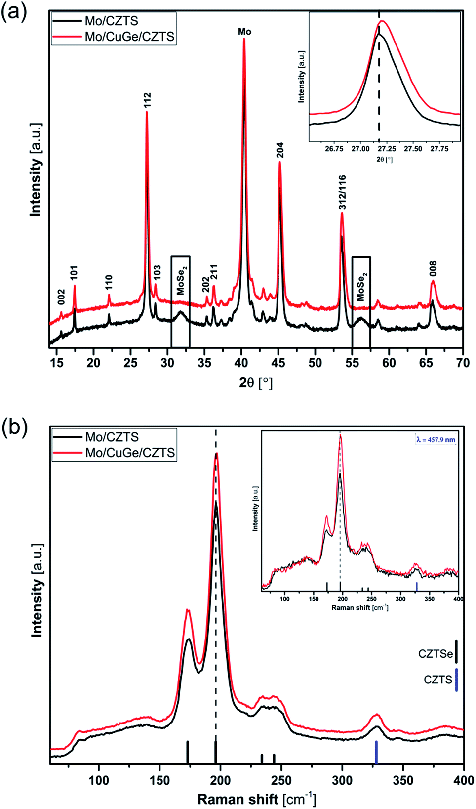 | ||
| Fig. 1 (a) X-ray diffraction (XRD) patterns and (b) Raman spectra of CZTSSe layers with and without 20 nm CuGe seed layer. | ||
Surface Raman spectra of the respective samples (Fig. 1(b)) were recorded as a complementary result to XRD to distinguish the well-known overlapping phases in the XRD reflections.29 The Raman spectra show the dominant characteristic peaks of kesterite phase (CZTSSe), whereas the sample with CuGe intermediate layer exhibits a slight blue shift in the kesterite characteristic peaks of only ≈0.5 cm−1, showing the same trend observed in the XRD patterns (Fig. 1(a)) as a consequence of Ge incorporation. Results from both excitation wavelengths show no noticeable characteristic peaks attributable to possible secondary phases (Fig. 1(b) and inset).
In order to obtain more information about the existence of secondary phases in depth, especially at the Mo/CZTSSe interface, depth-resolved Raman analysis was carried out in shallow angle cross sections (SACS) of the investigated samples, which were prepared by means of a focused ion beam setup. Further details about the SACS preparation and the advantages of this depth profiling approach can be found elsewhere.30,31
Fig. 2 shows the series of Raman spectra measured at different depths from the CZTS layer using 532 nm excitation wavelength.
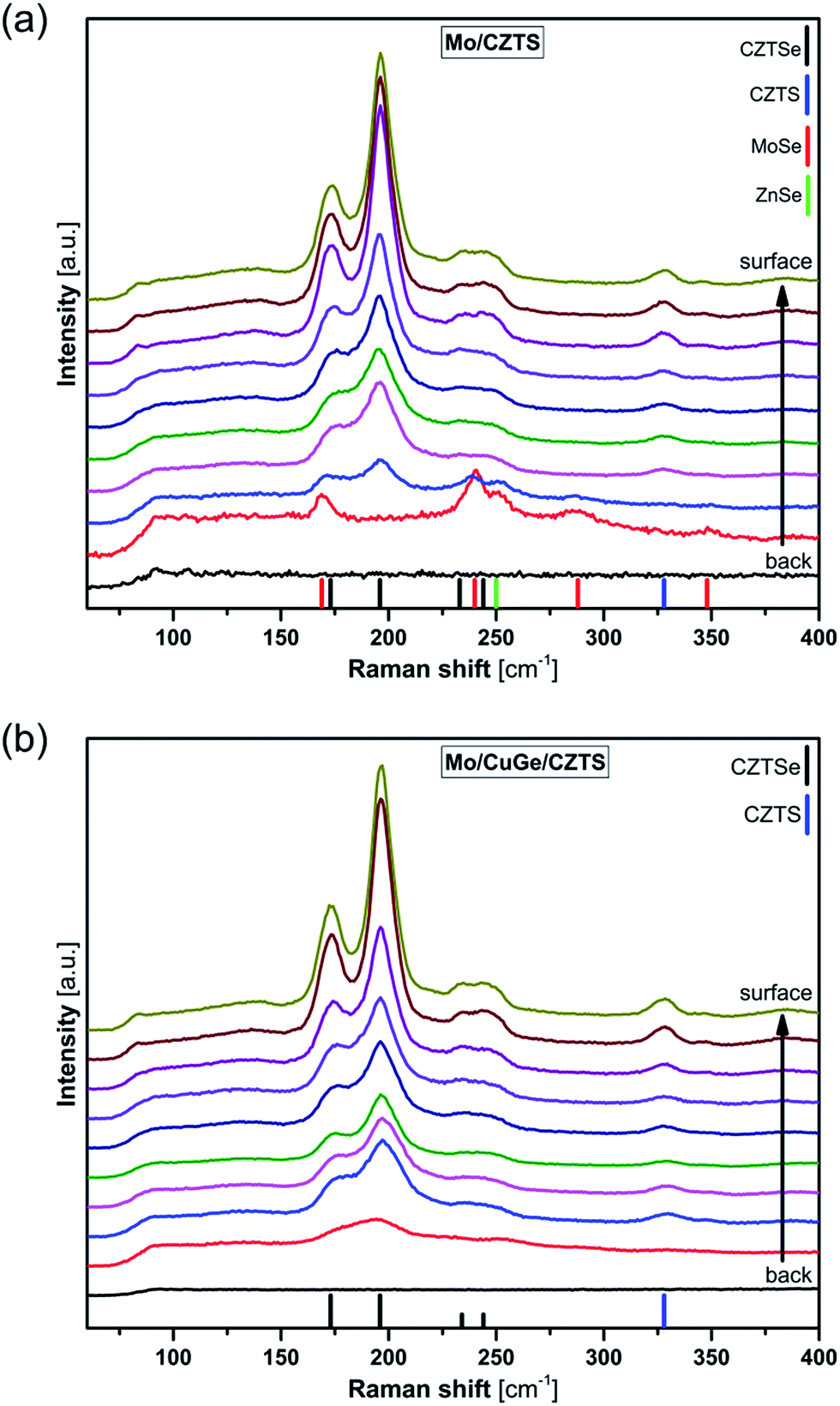 | ||
| Fig. 2 Depth resolved Raman spectra of CZTSSe layers grown from (a) SLG/Mo/CZTS and (b) SLG/Mo/CuGe/CZTS precursors. | ||
These measurements show mainly the dominant characteristic peaks of kesterite phase (CZTSSe) throughout the total depth of both investigated samples. However the Raman scattering signal decreases towards the back region, indicating that the crystal quality at the surface of the samples is higher than at the back region. Furthermore the sample prepared without CuGe (Fig. 2(a)) shows the occurrence of additional peaks at the Mo/CZTSSe interface at about 169 cm−1 and 240 cm−1, 288 cm−1 and 348 cm−1, which are the characteristic peaks of MoSe2 phase.32 Also a small ZnSe signal is visible at 250 cm−1 as an indication of the started decomposition reaction at the Mo/CZTSSe interface.10 This again confirms that the CuGe seed layer suppresses the formation of MoSe2 phase as stated earlier and consequently prevents the decomposition reaction at the Mo/CZTSSe interface. The CuGe seed layer prevents the direct contact between Mo and CZTSSe layer and additionally may hinder the diffusion of selenium into the Mo layer, thus inhibiting the decomposition and formation of secondary phases.
Fig. 3 shows a comparison between the typical SEM cross sections of the CZTSSe devices without and with 20 nm CuGe layer. The CZTSSe sample without CuGe intermediate layer (Fig. 3(a)) exhibits a bi-layer structure with a large grains containing top layer and a layer of small fine grains at the Mo/CZTSSe interface. However the CZTSSe sample obtained from the Mo/CuGe/CZTS stack (Fig. 3(b)) shows a tri-layer structure with large grain layers on the top and bottom of the CZTSSe absorber and a layer of small fine CZTSSe grains in the middle of the film.
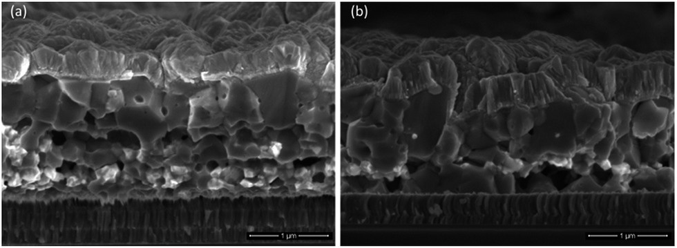 | ||
| Fig. 3 SEM cross section images of CZTSSe devices grown (a) without and (b) with 20 nm CuGe seed layer. | ||
This enhancement of grain growth at the Mo/CZTSSe interface could be directly related to the influence of the CuGe seed layer during the selenization process and thus the quality of the CZTSSe layer itself. An absorber layer with a large grain structure can be beneficial for device performance due to less grain boundaries, lower bulk defects and less carriers recombination.18,21
The current density–voltage (J–V) characteristics of the obtained CZTSSe devices are shown in Fig. 4(a). As indicated, the device efficiency was improved from 3.5% to 4.7% when inserting the 20 nm CuGe seed layer compared to the device without CuGe.
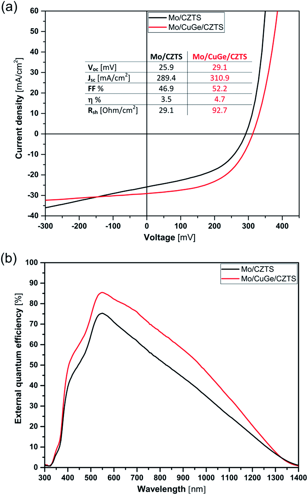 | ||
| Fig. 4 Device characteristics of the CZTSSe solar cells: (a) J–V characteristics and (b) EQE spectra of CZTSSe solar cells without and with 20 nm CuGe intermediate layer. | ||
The obtained device parameters show improvement of short circuit current (Jsc), open circuit voltage (Voc), fill factor (FF) and shunt resistance (Rsh) as given in the tabulated inset in Fig. 4(a). The overall improvement in the device parameters can be ascribed to the suppression of MoSe2 formation, hindering the subsequent decomposition reaction at the back interface, and accordingly the overall improvement of the quality of the CZTSSe absorber layer in combination with the beneficial effect of the Ge incorporation as discussed earlier.
The EQE spectra (Fig. 4(b)) are of triangular shape, whereby the deviations from the optimum can be linked to a current loss within the space charge region (SCR) (short wavelengths) as well as a lack in current collection (long wavelengths). The latter could be linked to a high doping concentration and hence small SCR width.33 Comparing both EQE spectra, the EQE of the device with CuGe shows a clear enhancement in both loss regimes. In the long wavelength region, this enhancement indicates a clear improvement in charge carrier collection within the CZTSSe absorber resulting from larger SCR width and a better overall quality of the CZTSSe absorber. The enhanced current collection is in agreement with the Jsc derived from the IV characterization.
For further investigating the impact of the CuGe seed layer on the electronic properties of the device C–V measurements were performed. From these we are able to estimate the doping density (NA), the built in potential (Vbi) and SCR width (W) in the CZTSSe absorber layers. The capacitance data in the Mott–Schottky plot (A2/C2 versus applied voltage, where A is the area of the cell) is shown in Fig. 5 and reveals a linear behavior for a broad voltage range, which allows the well-known extraction of the parameters NA and Vbi and W which are tabulated in Fig. 5 inset.34,35
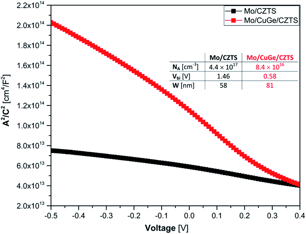 | ||
| Fig. 5 C–V measurements and extracted parameters for both CZTSSe layers. | ||
Comparing the difference in capacitive contribution of both cells with their IV characteristics, an enhanced type-inversion at the hetero interface due to lower doping concentration could be linked to a higher Voc. Moreover, the lower NA of the device with CuGe leads to a higher W resulting in a better current collection and thus the observed improvement in EQE spectra.
Conclusions
We have shown preparation of CZTSSe solar cells from a facile spray pyrolysis method, in absence of any toxic solvents, which allows for low cost and large area deposition in atmospheric conditions. For improving the performance of the obtained CZTSSe solar cells we have applied 20 nm CuGe seed layers onto SLG/Mo substrates to optimize the back contact interface region. Our experiments clearly show that CuGe seed layers can inhibit the formation of MoSe2 and the consequent decomposition reaction at the back contact interface during the annealing process. XRD and Raman analysis show a barely noticeable shift towards higher diffraction angles and wavenumbers, respectively, as an indication of slight Ge incorporation into the CZTSSe layer.The overall device performance was improved with an increase in the efficiency from 3.5% to 4.7% when inserting the 20 nm CuGe seed layer. EQE and C–V show an improvement in charge carrier collection within the CZTSSe absorber resulting from lower doping density, larger SCR width and better quality of the CZTSSe absorber.
We believe that these findings can be transferred to further CZTSSe processing techniques as a feasible way to suppress the formation of the MoSe2 during the annealing process and to simultaneously improve the overall quality of the absorber by incorporating small amounts of Ge into the CZTSSe layer.
Acknowledgements
The authors would like to thank Ulf Mikolajczak, Matthias Macke, Holger Koch and Thomas Madena for technical support and Jörg Ohland, Michael Richter and J. F. Lopez Salas for fruitful discussion. The work was funded by EWE AG, Oldenburg, Germany, and the BMBF (German Ministry of Education and Science), funding No. 03SF0530A (project “Free-Inca”). M. H. S. acknowledges the financial support from the Egyptian Ministry of Higher Education (MoHE) and the German Academic Exchange Service (DAAD) through German Egyptian Research Long-Term Scholarship “GERLS”. Colleagues at ZSW (Stuttgart, Germany), especially Erik Ahlswede, are acknowledged for supply of SLG/Mo substrates.Notes and references
- T. K. Todorov, K. B. Reuter and D. B. Mitzi, Adv. Mater., 2010, 22, E156 CrossRef CAS PubMed.
- D. B. Mitzi, O. Gunawan, T. K. Todorov, K. Wang and S. Guha, Sol. Energy Mater. Sol. Cells, 2011, 95, 1421 CrossRef CAS.
- J. Kim, H. Hiroi, T. K. Todorov, O. Gunawan, M. Kuwahara, T. Gokmen, D. Nair, M. Hopstaken, B. Shin, Y. S. Lee, W. Wang, H. Sugimoto and D. B. Mitzi, Adv. Mater., 2014, 26, 7427 CrossRef CAS PubMed.
- S. Siebentritt, Thin Solid Films, 2013, 535, 1 CrossRef CAS.
- I. Repins, C. Beall, N. Vora, C. DeHart, D. Kuciauskas, P. Dippo, B. To, J. Mann, W. C. Hsu, A. Goodrich and R. Noufi, Sol. Energy Mater. Sol. Cells, 2012, 101, 154 CrossRef CAS.
- S. W. Shin, S. M. Pawar, C. Y. Park, J. H. Yun, J.-H. Moon, J. H. Kim and J. Y. Lee, Sol. Energy Mater. Sol. Cells, 2011, 95, 3202 CrossRef CAS.
- T. Schnabel, M. Löw and E. Ahlswede, Sol. Energy Mater. Sol. Cells, 2013, 117, 324 CrossRef CAS.
- C. K. Miskin, W.-C. Yang, C. J. Hages, N. J. Carter, C. S. Joglekar, E. A. Stach and R. Agrawal, Prog. Photovoltaics, 2015, 23, 654 CAS.
- J. J. Scragg, T. Ericson, T. Kubart, M. Edoff and C. Platzer-Björkman, Chem. Mater., 2011, 23, 4625 CrossRef CAS.
- J. J. Scragg, J. T. Wätjen, M. Edoff, T. Ericson, T. Kubart and C. Platzer-Björkman, J. Am. Chem. Soc., 2012, 134, 19330 CrossRef CAS PubMed.
- X. Liu, Y. Feng, H. Cui, F. Liu, X. Hao, G. Conibeer, D. B. Mitzi and M. Green, Prog. Photovoltaics, 2016, 24, 879 Search PubMed.
- J. J. Scragg, T. Kubart, J. T. Watjen, T. Ericson, M. K. Linnarsson and C. Platzer-Björkman, Chem. Mater., 2013, 25, 3162 CrossRef CAS.
- T. Schnabel and E. Ahlswede, Sol. Energy Mater. Sol. Cells, 2017, 159, 290 CrossRef CAS.
- F. Liu, K. Sun, W. Li, C. Yan, H. Cui, L. Jiang, X. Hao and M. A. Green, Appl. Phys. Lett., 2014, 104, 051105 CrossRef.
- S. Lopez-Marino, M. Placidi, A. Perez-Tomas, J. Llobet, V. Izquierdo-Roca, X. Fontane, A. Fairbrother, M. Espindola-Rodriguez, D. Sylla, A. Perez-Rodriguez and E. Saucedo, J. Mater. Chem. A, 2013, 1, 8338 CAS.
- H. Cui, X. Liu, F. Liu, X. Hao, N. Song and C. Yan, Appl. Phys. Lett., 2014, 104, 041115 CrossRef.
- F. Zhou, F. Zeng, X. Liu, F. Liu, N. Song, C. Yan, A. Pu, J. Park, K. Sun and X. Hao, ACS Appl. Mater. Interfaces, 2015, 7, 22868 CAS.
- Z. Tong, K. Zhang, K. Sun, C. Yan, F. Liu, L. Jiang, Y. Lai, X. Hao and J. Li, Sol. Energy Mater. Sol. Cells, 2016, 144, 537 CrossRef CAS.
- S. Giraldo, M. Neuschitzer, T. Thersleff, S. Lopez-Marino, Y. Sanchez, H. Xie, M. Colina, M. Placidi, P. Pistor, V. Izquierdo-Roca, K. Leifer, A. Perez-Rodriguez and E. Saucedo, Adv. Energy Mater., 2015, 5, 1501070 CrossRef.
- D. B. Khadka, S. Y. Kim and J. H. Kim, RSC Adv., 2016, 6, 37621 RSC.
- S. Kim, K. M. Kim, H. Tampo, H. Shibata, K. Matsubara and S. Niki, Sol. Energy Mater. Sol. Cells, 2016, 144, 488 CrossRef CAS.
- M. Neuschitzer, J. Marquez, S. Giraldo, M. Dimitrievska, M. Placidi, I. Forbes, V. Izquierdo-Roca, A. Perez-Rodriguez and E. Saucedo, J. Phys. Chem. C, 2016, 120, 9661 CAS.
- Q. Shu, J.-H. Yang, S. Chen, B. Huang, H. Xiang, X.-G. Gong and S.-H. Wei, Phys. Rev. B: Condens. Matter Mater. Phys., 2013, 87, 115208 CrossRef.
- G. M. Ford, Q. Guo, R. Agrawal and H. W. Hillhouse, Chem. Mater., 2011, 23, 2626 CrossRef CAS.
- K. Biswas, S. Lany and A. Zunger, Appl. Phys. Lett., 2010, 96, 201902 CrossRef.
- S. Giraldo, T. Thersleff, G. Larramona, M. Neuschitzer, P. Pistor, K. Leifer, A. Perez-Rodriguez, C. Moisan, G. Dennler and E. Saucedo, Prog. Photovoltaics, 2016, 24, 1359 CAS.
- S. Lopez-Marino, Y. Sanchez, M. Placidi, A. Fairbrother, M. Espindola-Rodriguez, X. Fontane, V. Izquierdo-Roca, J. Lopez-Garcia, L. Calvo-Barrio, A. P. Rodriguez and E. Saucedo, Chem.–Eur. J., 2013, 19, 14814 CrossRef CAS PubMed.
- S. Bag, O. Gunawan, T. Gokmen, Y. Zhu and D. B. Mitzi, Chem. Mater., 2012, 24, 4588 CrossRef CAS.
- H. Yoo, R. A. Wibowo, A. Hölzing, R. Lechner, J. Palm, S. Jost, M. Gowtham, F. Sorin, B. Louis and R. Hock, Thin Solid Films, 2013, 535, 73 CrossRef CAS.
- C. Stroth, M. H. Sayed, M. Schuster, J. Ohland, I. Hammer-Riedel, M. S. Hammer, P. Wellmann, J. Parisi and L. Gütay, in IEEE 43rd Photovoltaic Specialists Conference PVSC, Portland, OR, 2016, pp. 0506–0511 Search PubMed.
- C. Stroth, M. H. Sayed, M. Schuster, J. Ohland, I. Hammer-Riedel, M. S. Hammer, P. Wellmann, J. Parisi and L. Gütay, J. Mater. Sci.: Mater. Electron., 2017 DOI:10.1007/s10854-017-6467-8.
- A. Redinger, K. Hönes, X. Fontane, V. Izquierdo-Roca, E. Saucedo, N. Valle, A. Perez-Rodriguez and S. Siebentritt, Appl. Phys. Lett., 2011, 98, 101907 CrossRef.
- D. Colombara, E. V. C. Robert, A. Crossay, A. Taylor, M. Guennou, M. Arasimowicz, J. C. B. Malaquias, R. Djemour and P. J. Dale, Sol. Energy Mater. Sol. Cells, 2014, 123, 220 CrossRef CAS.
- D. Abou-Ras, T. Kirchartz and U. Rau, Advanced Characterization Techniques for Thin Film Solar Cells, Wiley-VCH, Weinheim, 2011, p. 86 Search PubMed.
- S. S. Hegedus and W. N. Shafarman, Prog. Photovoltaics, 2004, 12, 155 CAS.
| This journal is © The Royal Society of Chemistry 2017 |