 Open Access Article
Inverse-architecture perovskite solar cells with 5,6,11,12-tetraphenylnaphthacene as a hole conductor†
Chengxin Wanga,
Hao Haoa,
Shufen Chen *a,
Kun Caoa,
Hongtao Yua,
Qin Zhanga,
Guangjian Wanb,
Wenjuan Shangac and
Wei Huang
 *ad
*ad
aKey Laboratory for Organic Electronics and Information Displays and Jiangsu National Synergetic Innovation Center for Advanced Materials, Nanjing University of Posts and Telecommunications, Nanjing 210023, China. E-mail: iamsfchen@njupt.edu.cn
bNanjing Engineering Research Center for Preparation and Application of Advanced Fiber Materials, Nanjing University of Posts and Telecommunications, Nanjing 210023, China
cState Key Laboratory on Integrated Optoelectronics, College of Electronic Science and Engineering, Jilin University, Changchun 130012, China
dKey Laboratory of Flexible Electronics and National Synergistic Innovation Center for Advanced Materials, Nanjing Tech University, Nanjing 211816, China
First published on 9th June 2017
Abstract
5,6,11,12-Tetraphenylnaphthacene (rub), an organic small molecular semiconductor widely used in organic field-effect transistors and organic light-emitting diodes, was introduced into MAPbI3-based inverse-architecture perovskite solar cells as a hole transport layer due to its high hole mobility, good hydrophobic properties, favourable highest occupied molecular orbital (HOMO), low-cost, and low-temperature treatment process of rub. A high open-circuit voltage of 0.96 V, short-circuit current of 22 mA cm−2, and power conversion efficiency of 14.3% were achieved in the inverted planar heterostructure perovskite solar cells based on the rub hole-transport layer due to the HOMO energy level matching between rub and MAPbI3, large hole conductivity of rub, and large crystalline grain size of MAPbI3 formed on rub.
1. Introduction
Organic–inorganic hybrid perovskite solar cells (PSCs) have been demonstrated as one of the most promising and fast growing photovoltaic technologies due to their high efficiency, various photovoltaic architectures, and low-cost manufacture.1–3 The power conversion efficiencies PCEs of PSCs based on the hybrid perovskite materials CH3NH3PbX3 (MAPbX3, X = Cl, Br, or I) have remarkably progressed over the past few years, even in planar heterojunction structures with simple device architectures and easy fabrication processes.4,5 The superior photoelectric conversion capability mainly originates from the unique optoelectronic properties, including extremely high optical absorption coefficient,6 excellent bipolar carrier transport ability,7,8 and low non-radiative recombination rates, of the organic–inorganic hybrid perovskite materials.In PSCs, the perovskite absorber is typically sandwiched between the electron and hole transport layers (ETL and HTL); thus, careful selection of both the ETL and HTL is critical for achieving high optoelectronic conversion efficiency due to their important roles in the separation and collection of the photogenerated charge carriers produced in the perovskites. Matching the lowest unoccupied molecular orbital (LUMO) of the ETL and the highest occupied molecular orbital (HOMO) of the HTL respectively with those of the perovskite absorber is beneficial for optimizing the open-circuit voltage (Voc) and dissociating excitons at the interfaces; moreover, high carrier mobilities of these carrier transport layers can effectively transport charge carriers towards the electrodes and avoid the hysteresis phenomenon. The commonly used ETLs include inorganic TiO2,9 ZnO,10 and organic [6,6]-phenyl-C61-butyric acid methyl ester (PC61BM);11 among these, PC61BM has a relatively high mobility of ∼10−4 cm2 V−1 s−1 and is widely used in inverse-architecture PSCs.12 Among the reported hole-transport materials e.g., CuI,13 CuSCN,14 CuInS2,15 CuOx,16 Cu-doped NiO,17 2,2′,7,7′-tetrakis-(N,N-di-p-methoxyphenylamine)-9,9′-spiro-bifluorene (spiro-OMeTAD),18 and poly(3,4-ethylene-dioxythiophene):poly(4-styrenesulfonate) (PEDOT:PSS),19 inorganic hole conductors display high hole mobilities, good chemical stability, and low-cost; however, the PSCs employing these inorganic hole conductors also show disadvantages such as low recombination resistance, high-temperature processing, and poor quality of perovskite film on these thick hole conductors. Kamat et al. first reported CuI as an HTL in PSCs and achieved a PCE of 6.0%.20 The low PCE was attributed to the higher recombination occurring at the CuI/perovskite interface. Then, Nazeeruddin et al. improved the PCE to 12.4% using CuSCN as a hole conductor in the conventional-architecture PSCs.21 CuSCN and NiO have also been explored in inverse-architecture PSCs with PCEs of 3.8% and 9.1%, respectively.22,23 Recently, Jen et al. have utilized Cu-doped NiO as a hole-extraction layer and acquired a PCE of 15.4%.24 However, the high-temperature or high-vacuum process used to prepare the NiOx film to achieve a high PCE cannot meet the requirements for the future development of solution-processable, low-cost, and mass-manufacturable solar cells.
In comparison with inorganic hole conductors, organic hole transport materials have universally low hole mobilities but have the advantages of an adjustable HOMO energy level and low-temperature treatment fabrication process. Among all of the organic hole transport materials including spiro-OMeTAD,25 poly[N,N′-bis(4-butylphenyl)-N,N′-bis(phenyl)benzidine] (poly-TPD),26 triazine-Th-OMeTPA,27 and polytriarylamine (PTAA),28 PEDOT:PSS is a well-known hole conductor and has been commonly used as an efficient interfacial layer for the modification of indium-tin oxide (ITO) anodes in organic light-emitting devices and organic solar cells.29–32 Since the first report on PEDOT:PSS in an inverse-architecture PSC by Chen et al.,33 many studies have been reported on the use of PEDOT:PSS for achieving high PCEs and a highest efficiency of 19.1% has been reported.34 However, PEDOT:PSS is not an ideal hole-transport material because of its inefficient electron-blocking capability and the detrimental effects of its intrinsic hygroscopic and acidic nature on the device stability. In addition, the HOMO level of PEDOT:PSS (−(4.9–5.2) eV, depending on the ratio of PEDOT to PSS) is lower than the valence band potential of CH3NH3PbI3 perovskite (∼−5.43 eV); thus, the potential energy loss at the CH3NH3PbI3/PEDOT:PSS interface decreases the built-in potential of the perovskite solar cells and thus generates a low Voc. Furthermore, the common combination of PEDOT:PSS with PC61BM as the hole and electron conductor is far from an optimal device structure due to the larger mobility of PC61BM (2.98 × 10⁻⁴ cm2 V−1 s−1) than that of PEDOT:PSS (1.0 × 10⁻⁴ cm2 V−1 s−1).35,36 Zhu et al. decreased the electron mobility of PC61BM comparable to that of PEDOT:PSS by doping PMMA into PC61BM and demonstrated a high PCE of 18.7%.37
For the abovementioned reasons, the development of alternative hole conductors to PEDOT:PSS is a promising avenue for further improving the performance of inverse-architecture PSCs as PEDOT:PSS likely does not represent an ideal hole-conducting material for this system. Clearly, a promising strategy to achieve high-performance PSCs with a large Voc and excellent device stability is to use an organic HTL with high HOMO level, hydrophobic property, and large hole mobility.
In this study, we employed a small-molecular organic semiconductor 5,6,11,12-tetraphenylnaphthacene (rubrene, abbreviated as rub) as the hole conductor in CH3NH3PbI3-based perovskite solar cells due to the following excellent properties of rub. First, as widely reported in organic field-effect transistors,38,39 rub has an extremely high hole mobility of ∼0.5 cm2 V−1 s−1, with which holes can be effectively transported and extracted from the photovoltaic devices. Moreover, rub has a favourable HOMO level (−5.06 eV) with respect to the valence band of perovskite (∼−5.43 eV), which is helpful for obtaining a high Voc. Moreover, rub is easily dissolved in conventional organic solvents such as chloroform and chlorobenzene, with the resulting rub film showing pretty good hydrophobic properties and preventing water vapor entering into the perovskite film. Notably, rub film has extremely low cost when compared with other organic HTLs such as spiro-OMeTAD and PEDOT:PSS; more importantly, it can be solution processed at a low treatment temperature of less than 110 °C, which is compatible with future manufacturing processes of large-area flexible solar cells.
With rub as a single-hole conductor, we manufactured CH3NH3PbI3-based PSCs and achieved the highest PCEs of 13.0% and 14.3% for the forward and reverse scans, respectively, which is higher than 12.4% (forward) and 12.7% (reverse) observed for a conventional PEDOT:PSS. Furthermore, we fabricated a group of PSCs with a bi-HTL of PEDOT:PSS/rub to replace the single rub layer and acquired higher PCEs of 13.7% and 14.4% for the forward and reverse scans, respectively. This study provides new opportunities for the choice of hole transport materials in perovskite solar cells.
2. Experimental details
2.1 Materials
Patterned ITO glasses with a sheet resistance of 7 Ω sq−1 and a thickness of 1.1 mm were purchased from Hua Yu United Technology Co. Ltd. Lead iodide (PbI2) and methylammonium iodide (MAI) were purchased from Sigma-Aldrich and Shanghai MaterWin New Materials Co. Ltd, respectively. PEDOT:PSS, rub, and PC61BM were purchased from Heraeus Materials Technology Co. Ltd., Banhe Technology Co. Ltd., and Nano-C, respectively. All solvents used were obtained from Sigma-Aldrich. All materials and solvents were directly used without further purification.2.2 Device fabrication
ITO glasses were washed with acetone, ethanol, and deionized water in sequence, followed by ultrasonic cleaning with deionized water, acetone, and ethanol for 15 min. After drying with high purity N2 and vacuum drying in an oven, the ITO substrates were treated with O3 for 15 min in an UV-ozone cleaner. Then, rub (or PEDOT:PSS) was spin-coated onto the patterned ITO glass substrates at 3000 rpm for 30 s (2000 rpm for 60 s for PEDOT:PSS), forming a 47 nm (50 nm for PEDOT:PSS) thick film, and then dried at 110 °C for 20 min (120 °C for 30 min for PEDOT:PSS). Similar to a single HTL, the bi-HTL of PEDOT:PSS/rub was treated via a two-step spin-coating process. Note that rub was dissolved in chlorobenzene at a concentration of 30 mg mL−1. To date, these HTL-coated glasses were moved into a glovebox to form a ∼300 nm MAPbI3 film via a one-step deposition method. The MAPbI3 solution was prepared by dissolving PbI2 and MAI (molar ratio of 1![[thin space (1/6-em)]](https://www.rsc.org/images/entities/char_2009.gif) :
:![[thin space (1/6-em)]](https://www.rsc.org/images/entities/char_2009.gif) 1, 40 wt%) into 1 mL of mixed solvent composed of dimethyl sulfoxide (DMSO) and gamma-butyrolactone (GBL) with a volume ratio of 3
1, 40 wt%) into 1 mL of mixed solvent composed of dimethyl sulfoxide (DMSO) and gamma-butyrolactone (GBL) with a volume ratio of 3![[thin space (1/6-em)]](https://www.rsc.org/images/entities/char_2009.gif) :
:![[thin space (1/6-em)]](https://www.rsc.org/images/entities/char_2009.gif) 7 and then stirring at 70 °C for 1 h. The perovskite precursor solution (60 μL) was spin-coated on the HTL at 2500 rpm for 90 s, and then, 300 μL of chlorobenzene was quickly dropped on the perovskite film. The as-prepared films were then annealed at 100 °C for 30 min on a hot plate. During the annealing process, the samples obviously changed from pale yellow to dark brown. After this, 20 mg mL−1 PC61BM in chlorobenzene was spin-coated onto the perovskite layer at 3000 rpm for 60 s in a N2 glovebox. Finally, all the samples were transferred to a vacuum chamber for 2,9-dimethyl-4,7-diphenyl-1,10-phenanthroline (BCP) and silver electrode evaporation. Herein, a 6 nm thick BCP and a 100 nm thick Ag were sequentially deposited onto the perovskite layer under a pressure of 6.0 × 10⁻⁵ Pa through a shadow mask with a defined device area of ∼0.1 cm2.
7 and then stirring at 70 °C for 1 h. The perovskite precursor solution (60 μL) was spin-coated on the HTL at 2500 rpm for 90 s, and then, 300 μL of chlorobenzene was quickly dropped on the perovskite film. The as-prepared films were then annealed at 100 °C for 30 min on a hot plate. During the annealing process, the samples obviously changed from pale yellow to dark brown. After this, 20 mg mL−1 PC61BM in chlorobenzene was spin-coated onto the perovskite layer at 3000 rpm for 60 s in a N2 glovebox. Finally, all the samples were transferred to a vacuum chamber for 2,9-dimethyl-4,7-diphenyl-1,10-phenanthroline (BCP) and silver electrode evaporation. Herein, a 6 nm thick BCP and a 100 nm thick Ag were sequentially deposited onto the perovskite layer under a pressure of 6.0 × 10⁻⁵ Pa through a shadow mask with a defined device area of ∼0.1 cm2.
2.3 Device characterization
The morphology of the perovskite layer was obtained using a Hitachi S-4800 field emission scanning electron microscope (SEM) and a Bruker atomic force microscope (AFM). The crystal structures of the MAPbI3 thin films were characterized using the Bruker D8 ADVANCE X-ray diffraction (XRD) equipment. The thicknesses of the PEDOT:PSS, rub, perovskite, and PC61BM films were determined using a Bruker DektakXT Stylus Profiler. The current density–voltage (J–V) characterization of the perovskite solar cells was carried out using a Keithley 2400 source meter under a simulated AM 1.5 illumination (100 mW cm−2, Oriel Sol3A 94023A Class Solar Simulator) at a scan rate of 200 mV s−1. The UV-vis absorption spectra of the perovskite films and the transmissivity of different HTLs were obtained using a PerkinElmer Lambda 650S spectrophotometer with an excitation wavelength of 400 nm. The photoluminescence measurements were carried out using a Horiba Fluoromax 4 spectrometer. The impedance characteristics of the devices were measured via a Wayne kerr 6500B analyzer. The surface potential of the HTLs (PEDOT:PSS or rub) was measured using a Cypher S atomic force microscope.3. Results and discussion
3.1 The influence of rub on the optical and electrical properties of the perovskite films
Fig. 1(a) illustrates the structural image of the present inverse-architecture planar perovskite solar cells, in which a rub layer was applied between the ITO electrode and perovskite photoactive layer to work as an efficient hole selective layer. Rub was chosen as it has extremely high hole mobility (∼0.5 cm2 V−1 s−1) and favourable HOMO level (−5.06 eV). In the control device, rub was replaced with the conventional PEDOT:PSS as the HTL, whereas for the bi-HTL device, rub was replaced with PEDOT:PSS/rub. Scanning Kelvin probe microscopy (SKPM) was employed to determine the surface potential (HOMO level) of the PEDOT:PSS or rub, which helped to reveal the band bending at the perovskite/PEDOT:PSS or perovskite/rub interface in the energy level diagram. The two-dimensional surface potential distributions obtained for the PEDOT:PSS and rub films are shown in Fig. S1.† The HOMO levels of PEDOT:PSS and rub were −4.88 and −5.06 eV, respectively, which were calculated using the formula of φs = φTip + eVCPD and are summarized in Table S1.† Herein, φs is the surface potential of the sample, φTip is the tip potential of the yttrium probe, and VCPD is the contact potential difference between the sample and the probe. As observed from the energy level diagram shown in Fig. 1(b), higher HOMO (−5.06 eV) of rub than that of PEDOT:PSS (−4.88 eV) helps to reduce the potential energy loss at the CH3NH3PbI3/HTL interface, and thus, use of rub may generate a higher Voc in our PSCs. In addition, the hole and electron conductivities of rub and PEDOT:PSS were calculated using the direct current conductivity equation of I = σ0Ad−1V by designing single-hole and single-electron devices.40 The corresponding structures of the single-hole and single-electron device were ITO/PEDOT:PSS (65 nm) or rub (166 nm)/MoO3 (25 nm)/Ag and ITO/LiF (5 nm)/PEDOT:PSS (65 nm) or rub (166 nm)/LiF (0.8 nm)/Al, as shown in Fig. 2. From the measured electrical properties (Fig. 2(c) and (d)), the hole and electron conductivities of rub were calculated to be 4.96 × 10⁻² and 1.55 × 10⁻⁵ mS cm−1, respectively, whereas they were 3.66 × 10⁻³ and 1.01 × 10⁻³ mS cm−1 for PEDOT:PSS, respectively. Note that the hole conductivity of 4.96 × 10⁻² mS cm−1 for rub was much larger than 3.66 × 10⁻³ mS cm−1 of PEDOT:PSS, demonstrating a more efficient hole transport in the rub-based PSCs. In addition, the extremely low electron conductivity of rub indicates that the electron transport via rub towards the anode is almost impossible.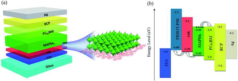 | ||
| Fig. 1 (a) The structural diagram of our perovskite solar cells and (b) the energy levels of the main components. | ||
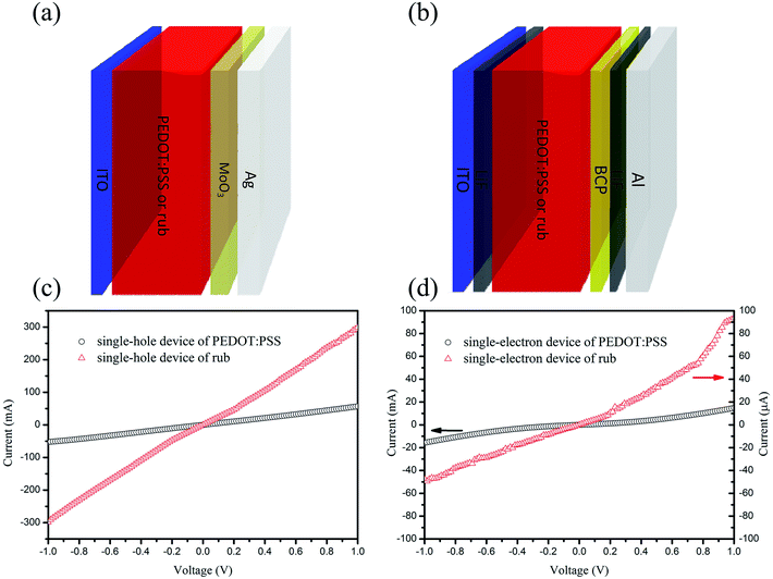 | ||
| Fig. 2 The structures of (a) single-hole and (b) single-electron devices based on PEDOT:PSS or rub. The current–voltage curves obtained for the (c) single-hole and (d) single-electron devices. | ||
Before introducing rub into the perovskite solar cell, the effect of the optical properties of rub on the perovskite layer was first studied. Fig. 3(a) illustrates the transmissivity characteristics of different HTLs. It can be clearly observed that the rub film has a weak absorption in the visible region, showing a high transmissivity of 87% at 550 nm. While for the PEDOT:PSS layer and the PEDOT:PSS/rub bi-HTL, the transmissivities exhibit a slight decline due to the absorption of PEDOT:PSS in the visible and near-infrared region. The influences of the HTLs on the absorption of the perovskite layer were also investigated, as illustrated in Fig. 3(b). Similar absorption spectra confirm that the absorption of these HTLs was negligible when compared with that of the perovskite layer.
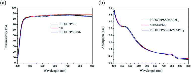 | ||
| Fig. 3 (a) The transmissivity curves obtained for PEDOT:PSS, rub and PEDOT:PSS/rub. (b) The UV-vis absorption spectra of perovskite on the different HTLs. | ||
3.2 The morphology and quality of the perovskite films
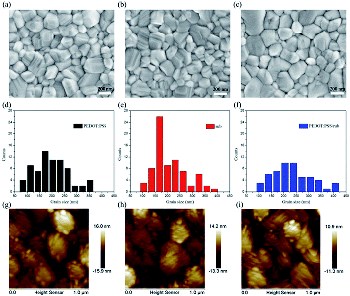
Fig. 4(a–c) displays the scanning electron microscopy (SEM) images of the surface morphology of the perovskite films on the different HTLs. It is notable that the average crystalline grain size of the perovskite on the rub substrates (208 nm and 234 nm on rub and rub/PEDOT:PSS, respectively) is much larger than that on the PEDOT:PSS substrates (198 nm), as shown in the panels d, e, and f. The non-wetting surface of rub, as shown in Fig. S2,† is beneficial for grain growth because of the lower nucleus density and less dragging force.41,42 The larger grain size observed on the rub substrates is of importance in suppressing the grain boundary traps to obtain better device efficiency.43 The panels g, h, and i of Fig. 4 show the surface morphology of the perovskite films on different HTLs obtained by atomic force microscopy (AFM) in the tapping mode. The calculated surface roughnesses (root mean square, RMS) of the perovskite films are 3.83 nm and 3.19 nm for the samples on rub and PEDOT:PSS/rub, respectively, which are slightly smaller than 4.32 nm observed for those directly deposited on PEDOT:PSS.Fig. 5 shows the X-ray diffraction (XRD) patterns of the CH3NH3PbI3 films grown on ITO, PEDOT:PSS, rub, and rub/PEDOT:PSS. The peaks at 14.1°, 28.4°, and 42.1° were attributed to the (110), (220), and (330) faces of the CH3NH3PbI3 perovskite crystalline structure, respectively.44,45 It was observed that all these perovskite diffraction peaks became significantly enhanced when the perovskite film were formed on rub, which was indicative of the improvement in the crystalline properties of the CH3NH3PbI3 film. The high crystalline quality of the perovskite finally contributes to high short-circuit current (Jsc) and thus a high PCE.
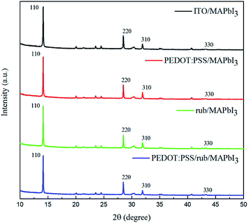 | ||
| Fig. 5 The XRD patterns of the MAPbI3 films on the ITO, PEDOT:PSS, rub and PEDOT:PSS/rub substrates. | ||
3.3 The performance of the PSCs
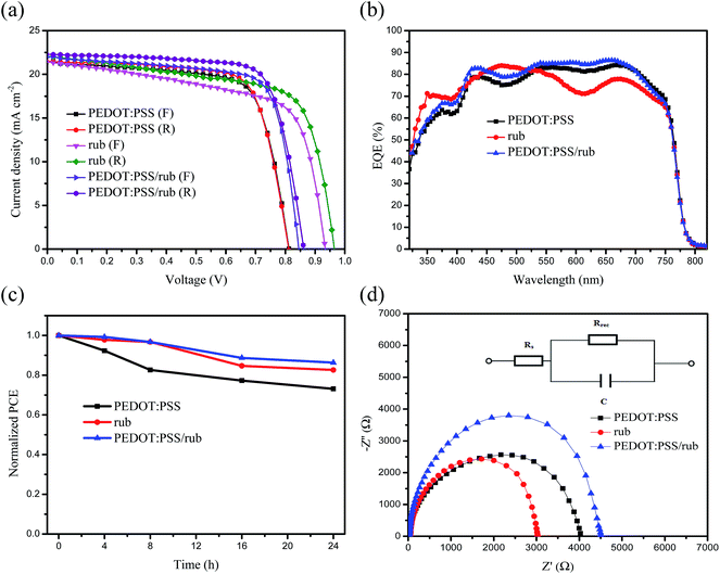
A batch of inverse-architecture planar heterostructure PSCs was fabricated with different HTLs with their J–V curves illustrated in Fig. 6(a) and parameters summarized in Table 1. It was found that distinct HTLs have significant impacts on the device performance. As was expected, PSCs using rub as the hole conductor yielded a large Voc of 0.96 V because of the matched HOMO energy levels between rub and the perovskite, which was larger than 0.81 V found in the PSCs with the PEDOT:PSS HTL. Due to large hole conductivity of rub and improved crystalline quality of the perovskite, the Jsc (22.0 mA cm−2) in the rub-based PSCs was slightly better than 21.4 mA cm−2 found in the PEDOT:PSS-based PSCs. Despite a decrease in the filling factor (FF) from 73.1% to 67.5%, the rub-based PSCs showed a high PCE of 14.3%, which was slightly larger than 12.7% found in the PEDOT:PSS-based PSCs. It maintains a high Jsc (22.2 mA cm−2) in the bi-HTL devices, whereas the Voc in these devices present a compromise between the Vocs in the rub-based and that in the PEDOT:PSS-based PSCs. The resulting PCE reaches 14.4% in the PEDOT:PSS/rub bilayer devices, which is the best among the three groups of PSCs studied herein, as further demonstrated by the external quantum efficiency (EQE) curves shown in Fig. 6(b). It is noteworthy that there exist very small differences for both the current and PCE in the forward and reverse scanning directions (Table 1), indicating an extremely weak hysteresis in all the devices with good crystallinity and phase purity. The statistics on the PCE distribution (Fig. S3†) demonstrated the reliability and repeatability of the PCE enhancement with the use of the rub HTL in the photovoltaic devices. The stability of the cells with different HTLs was also investigated. Note that the as-fabricated devices with different HTLs were stored in an air atmosphere at 25 °C and a humidity of 35% without further encapsulation. From the normalized power conversion efficiency of the devices based on different HTLs as a function of storage time shown in Fig. 6(c), it could be seen that the rub-based and PEDOT:PSS/rub-based devices maintained 82.6% and 86.3% of the initial efficiency when these perovskite solar cells were stored in air atmosphere for 24 hours, better than 73.1% found for the PEDOT:PSS-based device; this indicates that the good hydrophobic properties of rub prevent water vapor entering into the perovskite film.| HTL | Scan direction | Jsc (mA cm−2) | Voc (V) | FF (%) | PCE (%) |
|---|---|---|---|---|---|
| PEDOT:PSS | Forward | 21.5 | 0.81 | 71.2 | 12.4 |
| Reverse | 21.4 | 0.81 | 73.1 | 12.7 | |
| rub | Forward | 21.4 | 0.93 | 65.1 | 13.0 |
| Reverse | 22.0 | 0.96 | 67.5 | 14.3 | |
| PEDOT:PSS/rub | Forward | 22.1 | 0.85 | 73.4 | 13.7 |
| Reverse | 22.2 | 0.86 | 74.9 | 14.4 |
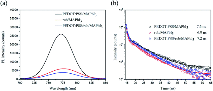
It is reasonable to believe that rub plays an important role in carrier transport and exciton dissociation; thus, it will display high FF in the rub-based devices. However, reduced FF value was observed in all the devices with a single rub as the hole transport layer. To explore the charge transfer at the interface between the HTLs and the perovskite layer, the perovskite films on the rub layer and those on the PEDOT:PSS layer were fabricated to measure the steady-state and time-resolved transient photoluminescence (PL) spectra. Fig. 7 presents the steady-state and time-resolved transient PL spectra of PEDOT:PSS/perovskite, rub/perovskite, and PEDOT:PSS/rub/perovskite. It can be seen from Fig. 7(a) that the PEDOT:PSS/MAPbI3 film has a strong PL response, whereas the PL intensities of the rub/MAPbI3 film and the PEDOT:PSS/rub/MAPbI3 film obviously decrease. This phenomenon indicates that rub is more effective in transferring charge carriers than PEDOT:PSS. The time-resolved PL measurements also confirm this indication. The PL lifetimes of these two samples were fitted with a bi-exponential decay function including a fast decay and a slow decay process, of which the fast decay process is a consequence of the radiative decay of the free carriers in the perovskite layer and the slow decay process is ascribed to the hole carriers transported from the perovskite layer to the HTLs. The fitted parameters are summarized in Table S2.† The lifetimes that represent a slow decay process are 7.6 ns, 6.9 ns, and 7.2 ns for PEDOT:PSS/perovskite, rub/perovskite, and PEDOT:PSS/rub/perovskite, respectively, which are in agreement with the steady-state PL results.
To further understand the influence of the rub on the devices, electrochemical impedance spectroscopy (EIS) measurements for the perovskite solar cells with different HTLs were carried out with the their Nyquist plots shown in Fig. 6(d). Recombination processes are present in all photovoltaic devices; moreover, the arc observed in the low-frequency region of the Nyquist plots of the perovskite solar cells is associated with the recombination process, which is often described by the recombination resistance (Rrec) generated at these contact interfaces inside the rub/perovskite/PC61BM/BCP structure. Since the recombination rate is inversely proportional to Rrec, a high Rrec represents less recombination and sufficient dissociation of carriers at these interfaces. However, the Rrec (362 Ω cm2) shows a slight decrease in the PSCs fabricated with the rub HTL, indicating that serious recombination still occurs at the interfaces of rub/perovskite or PEDOT:PSS/rub although a faster charge carrier transfer process at this interface and a larger hole mobility of rub results in a decreased FF. However, the bi-HTL PSC shows larger Rrec (569 Ω cm2) than the PEDOT:PSS-based PSC (435 Ω cm2), excluding the significant recombination at the interface of PEDOT:PSS/rub. This result indicates that a better film morphology of rub was formed on PEDOT:PSS than that directly formed on an ITO electrode.
4. Conclusions
In summary, rub, a widely used organic small molecular semiconductor in organic field-effect transistors and organic light-emitting diodes, was introduced into inverted perovskite solar cells as a hole transport layer to replace the conventional PEDOT:PSS. A high Voc of 0.96 V, Jsc of 22.0 mA cm−2, and PCE of 14.3% were achieved in our inverted planar heterostructure perovskite solar cells based on the rub hole transport layer due to the HOMO energy level matching between rub and MAPbI3, large hole conductivity of rub, and large crystalline grain size of MAPbI3 on rub. Our experimental results further demonstrate that the PEDOT:PSS/rub bilayer as the hole transport layer exhibits a higher PCE of 14.4% in the inverted perovskite solar cells due to the better film quality of rub and reduced recombination at the interface of rub/perovskite. In comparison with other organic hole conductors (e.g., PEDOT:PSS, spiro-OMeTAD, etc.), rub has bright prospects for applications in planar heterostructure perovskite solar cells due to its extremely low-cost and low-temperature treatment process. A future work is to reduce the exciton/carrier recombination at the rub/perovskite interface and enhance FF via improvement of the film quality of rub.Acknowledgements
The authors acknowledge the financial support received from the National Foundation for Science and Technology Development (973 project, Grant No. 2015CB932202), the National Natural Science Foundation of China (Grant No. 61274065, 51173081, 61136003 and BZ2010043), the NSF of the Higher Education Institutions of Jiangsu Province (Grant No. SJ209003), the Natural Science Foundation of Jiangsu Province (Grant No. BM2012010), the Science Fund for Distinguished Young Scholars of Jiangsu Province of China (Grant No. BK20160039), the Priority Academic Program Development of Jiangsu Higher Education Institutions (Grant No. YX030001), the Jiangsu National Synergetic Innovation Center for Advanced Materials, the Synergetic Innovation Center for Organic Electronics and Information Displays, the Ordinary University Graduate Student Practical Innovation Projects of Jiangsu Province (Grant No. SJLX15_0390), and the Open Foundation from Jilin University (Grant No. IOSKL2015KF32).Notes and references
- D. Q. Bi, C. Y. Yi, J. S. Luo, J.-D. Décoppet, F. Zhang, S. M. Zakeeruddin, X. Li, A. Hagfeldt and M. Grätzel, Nat. Energy, 2016, 142, 16142 CrossRef.
- F. Fu, T. Feurer, T. Jäger, E. Avancini, B. Bissig, S. Yoon, S. Buecheler and A. N. Tiwari, Nat. Commun., 2015, 6, 8932 CrossRef CAS PubMed.
- J. T.-W. Wang, J. M. Ball, E. M. Barea, A. Abate, J. A. Alexander-Webber, J. Huang, M. Saliba, I. Mora-Sero, J. Bisquert, H. J. Snaith and R. J. Nicholas, Nano Lett., 2014, 14, 724–730 CrossRef CAS PubMed.
- D. Y. Liu and T. L. Kelly, Nat. Photonics, 2013, 342, 133–138 CrossRef.
- H. Hu, D. Wang, Y. Y. Zhou, J. L. Zhang, S. L. Lv, S. P. Pang, X. Chen, Z. H. Liu, N. P. Padtureb and G. L. Cui, RSC Adv., 2014, 4, 28964–28967 RSC.
- W.-J. Yin, T. T. Shi and Y. F. Yan, Adv. Mater., 2014, 26, 4653–4658 CrossRef CAS PubMed.
- S. D. Stranks, G. E. Eperon, G. Grancini, C. Menelaou, M. J. P. Alcocer, T. Leijtens, L. M. Herz, A. Petrozza and H. J. Snaith, Science, 2013, 342, 341–344 CrossRef CAS PubMed.
- G. C. Xing, N. Mathews, S. Y. Sun, S. S. Lim, Y. M. Lam, M. Grätzel, S. Mhaisalkar and T. C. Sum, Science, 2013, 342, 344–347 CrossRef CAS PubMed.
- J. H. Heo, S. H. Im, J. H. Noh, T. N. Mandal, C.-S. Lim, J. A. Chang, Y. H. Lee, H.-J. Kim, A. Sarkar, M. K. Nazeeruddin, M. Grätzel and S. I. Seok, Nat. Photonics, 2013, 80, 486–491 CrossRef.
- X. Dong, H. W. Hu, B. C. Lin, J. N. Ding and N. Y. Yuan, Chem. Commun., 2014, 50, 14405–14408 RSC.
- P. Docampo, J. M. Ball, M. Darwich, G. E. Eperon and H. J. Snaith, Nat. Commun., 2013, 4, 2761 Search PubMed.
- S.-M. Dai, H.-R. Tian, M.-L. Zhang, Z. Xing, L.-Y. Wang, X. Wang, T. Wang, L.-L. Deng, S.-Y. Xie, R.-B. Huang and L.-S. Zheng, J. Power Sources, 2017, 339, 27–32 CrossRef CAS.
- G. A. Sepalage, S. Meyer, A. Pascoe, A. D. Scully, F. Z. Huang, U. Bach, Y.-B. Cheng and L. Spiccia, Adv. Funct. Mater., 2015, 25, 5650–5661 CrossRef CAS.
- S. Y. Ye, W. H. Sun, Y. L. Li, W. B. Yan, H. T. Peng, Z. Q. Bian, Z. W. Liu and C. H. Huang, Nano Lett., 2015, 15, 3723–3728 CrossRef CAS PubMed.
- C. Chen, C. X. Li, F. M. Li, F. Wu, F. R. Tan, Y. Zhai and W. F. Zhang, Nanoscale Res. Lett., 2014, 9, 457 CrossRef PubMed.
- W. H. Sun, Y. L. Li, S. Y. Ye, H. X. Rao, W. B. Yan, H. T. Peng, Y. Li, Z. W. Liu, S. F. Wang, Z. J. Chen, L. X. Xiao, Z. Q. Bian and C. H. Huang, Nanoscale, 2016, 8, 10806–10813 RSC.
- M. H. Liu, Z. J. Zhou, P. P. Zhang, Q. W. Tian, W. H. Zhou, D. X. Kou and S. X. Wu, Opt. Express, 2016, 24, A1349–A1359 CrossRef PubMed.
- J. Lee, M. M. Menamparambath, J.-Y. Hwang and S. Baik, ChemSusChem, 2015, 8, 2358–2362 CrossRef CAS PubMed.
- Y. Wu, J. Y. Wang, X. Q. Qiu, R. Q. Yang, H. M. Lou, X. C. Bao and Y. Li, ACS Appl. Mater. Interfaces, 2016, 8, 12377–12383 CAS.
- J. A. Christians, R. C. M. Fung and P. V. Kamat, J. Am. Chem. Soc., 2014, 136, 758–764 CrossRef CAS PubMed.
- P. Qin, S. Tanaka, S. Ito, N. Tetreault, K. Manabe, H. Nishino, M. K. Nazeeruddin and M. Grätzel, Nat. Commun., 2014, 5, 3834–3840 CAS.
- A. S. Subbiah, A. Halder, S. Ghosh, N. Mahuli, G. Hodes and S. K. Sarkar, J. Phys. Chem. Lett., 2014, 5, 1748–1753 CrossRef CAS PubMed.
- Z. L. Zhu, Y. Bai, T. Zhang, Z. K. Liu, X. Long, Z. H. Wei, Z. L. Wang, L. X. Zhang, J. N. Wang, F. Yan and S. H. Yang, Angew. Chem., Int. Ed., 2014, 53, 12571–12575 CAS.
- J. H. Kim, P. W. Liang, S. T. Williams, N. Cho, C. C. Chueh, M. S. Glaz, D. S. Ginger and A. K.-Y. Jen, Adv. Mater., 2015, 27, 695–701 CrossRef CAS PubMed.
- Z. Hawash, L. K. Ono and Y. B. Qi, Adv. Mater. Interfaces, 2016, 3, 1600117 CrossRef.
- O. Malinkiewicz, A. Yella, Y. H. Lee, G. M. Espallargas, M. Graetzel, M. K. Nazeeruddin and H. J. Bolink, Nat. Photonics, 2014, 8, 128–132 CrossRef CAS.
- K. Do, H. Choi, K. Lim, H. Jo, J. W. Cho, M. K. Nazeeruddinc and J. Ko, Chem. Commun., 2014, 50, 10971–10974 RSC.
- Q. Wang, C. Bi and J. S. Huang, Nano Energy, 2015, 15, 275–280 CrossRef CAS.
- M. M. De Kok, M. Buechel, S. I. E. Vulto, P. Van De Weijer, E. A. Meulenkamp, S. H. P. M. De Winter, A. J. G. Mank, H. J. M. Vorstenbosch, C. H. L. Weijtens and V. Van Elsbergen, Phys. Status Solidi A, 2004, 201, 1342–1359 CrossRef CAS.
- D. A. Mengistie, P.-C. Wang and C.-W. Chu, J. Mater. Chem. A, 2013, 1, 9907–9915 Search PubMed.
- H. Park, Y. M. Shi and J. Kong, Nanoscale, 2013, 5, 8934–8939 RSC.
- F. Liu, Z. C. Zhou, C. Zhang, T. Vergote, H. J. Fan, F. Liu and X. Z. Zhu, J. Am. Chem. Soc., 2016, 138, 15523–15526 CrossRef CAS PubMed.
- J.-Y. Jeng, Y.-F. Chiang, M.-H. Lee, S.-R. Peng, T.-F. Guo, P. Chen and T.-C. Wen, Adv. Mater., 2013, 25, 3727–3732 CrossRef CAS PubMed.
- J. T.-W. Wang, Z. Wang, S. Pathak, W. Zhang, D. W. deQuilettes, F. Wisnivesky-Rocca-Rivarola, J. Huang, P. K. Nayak, J. B. Patel, H. A. Mohd Yusof, Y. Vaynzof, R. Zhu, I. Ramirez, J. Zhang, C. Ducati, C. Grovenor, M. B. Johnston, D. S. Ginger, R. J. Nicholas and H. J. Snaith, Energy Environ. Sci., 2016, 9, 2892–2901 CAS.
- C. Y. Kuang, G. Tang, T. G. Jiu, H. Yang, H. B. Liu, B. R. Li, W. N. Luo, X. D. Li, W. J. Zhang, F. S. Lu, J. F. Fang and Y. L. Li, Nano Lett., 2015, 15, 2756–2762 CrossRef CAS PubMed.
- A. E. Labban, H. Chen, M. Kirkus, J. Barbe, S. D. Gobbo, M. Neophytou, I. McCulloch and J. Eid, Adv. Energy Mater., 2016, 6, 1502101 CrossRef.
- K. Chen, Q. Hu, T. H. Liu, L. C. Zhao, D. Y. Luo, J. Wu, Y. F. Zhang, W. Zhang, F. Liu, T. P. Russell, R. Zhu and Q. H. Gong, Adv. Mater., 2016, 28, 10718–10724 CrossRef CAS PubMed.
- S. K. Park, T. N. Jackson, J. E. Anthony and D. A. Mourey, Appl. Phys. Lett., 2007, 91, 063514 CrossRef.
- C. D. Sheraw, T. N. Jackson, D. L. Eaton and J. E. Anthony, Adv. Mater., 2003, 15, 2009–2011 CrossRef CAS.
- J. Obrzut and K. A. Page, Phys. Rev. B: Condens. Matter Mater. Phys., 2009, 80, 195211 CrossRef.
- Z. G. Xiao, C. Bi, Y. C. Shao, Q. F. Dong, Q. Wang, Y. B. Yuan, C. G. Wang, Y. L. Gao and J. S. Huang, Energy Environ. Sci., 2014, 7, 2619–2623 CAS.
- C. Bi, Y. C. Shao, Y. B. Yuan, Z. G. Xiao, C. G. Wang, Y. L. Gao and J. S. Huang, J. Mater. Chem. A, 2014, 2, 18508–18514 CAS.
- C. Bi, Y. C. Shao, Q. Wang, Y. B. Yuan, Z. G. Xiao and J. S. Huang, Nat. Commun., 2015, 6, 7747 CrossRef CAS PubMed.
- M. M. Lee, J. Teuscher, T. Miyasaka, T. N. Murakami and H. J. Snaith, Science, 2012, 338, 643–647 CrossRef CAS PubMed.
- M. Liu, M. B. Johnston and H. J. Snaith, Nature, 2013, 501, 395–398 CrossRef CAS PubMed.
Footnote |
| † Electronic supplementary information (ESI) available. See DOI: 10.1039/c7ra02496g |
| This journal is © The Royal Society of Chemistry 2017 |

