 Open Access Article
Quantitative measurement of transport properties: Ag-doped nanocrystalline CdS thin films
Baljinder Singhab,
Janpreet Singhb,
Ramneek Kaurc,
R. K. Moudgila and
S. K. Tripathi *b
*b
aDepartment of Physics, Kurukshetra University, Kurukshetra-136119, India
bDepartment of Physics, Panjab University, Chandigarh-160014, India. E-mail: surya@pu.ac.in; surya_tr@yahoo.com; Fax: +91-172-2783336; Tel: +91-172-2534462
cDepartment of Physics, Akal University, Talwandi Sabo-151302, India
First published on 23rd November 2017
Abstract
This work highlights the transport properties of undoped and Ag doped nc-CdS thin films for optoelectronic devices. nc-CdS, nc-CdS:Ag 1% and nc-CdS:Ag 5% thin films were prepared by the thermal vacuum evaporation method. X-ray diffraction and scanning electron microscope studies show that the Ag doping affects the structural morphology of the films and the average grain size decreases at low Ag doping concentration whereas it increases at high Ag doping concentration in nc-CdS thin films. We have presented a study for the evaluation of the transport parameters like the drift mobility, recombination lifetime of carriers and mobility–lifetime product of charge carriers. Time-of-flight, steady-state photo-conductivity, and steady-state photocarrier Grating techniques are utilized to measure the mobility, mobility–lifetime product and ambipolar diffusion length of charge carriers. The mobility of electrons (µe) and holes (µh), diffusion length (L) and mobility–lifetime (µτ)h product of holes varied strongly and systematically with grain-size. The mobility–lifetime (µτ)e product of majority carriers has been estimated from the temperature dependence of the photoconductivity, which increases with increasing temperature and doping. For nc-CdS:Ag 5%, µe, µh increases over two orders of magnitude and (µτ)e increases over an order of magnitude compared to that of nc-CdS. The recombination lifetime of carriers increased significantly in doped and undoped nc-CdS as compared to bulk CdS. We observe that the transport properties increase significantly with higher Ag doping concentration in nc-CdS thin films.
Introduction
Nanocrystalline semiconductor thin films have attracted a great deal of attention in novel optoelectronic devices due to their unique physical, optical and electrical properties compared to their bulk counterparts. Their properties can be easily tuned by altering the nanoparticle size and their composition and by introducing dopants. Among the II–VI semiconductors, cadmium sulfide (CdS), a direct band-gap (2.42 eV) semiconductor, has been considered as a promising material for constructing optoelectronic devices. Nanocrystalline cadmium sulfide (nc-CdS) thin films offer numerous technological applications in electronic devices,1 window layers in heterojunction solar cells,2 Schottky diodes,3 optoelectronic switches,4 photo detectors,5 gas sensors,6 etc. An extensive variety of film deposition techniques such as vacuum evaporation,7 close spaced sublimation,8 sputtering,9 spray pyrolysis,10 photochemical synthesis,11 the microwave method,12 and chemical bath deposition13 are utilized to fabricate CdS thin films. Out of these, vacuum evaporation is renowned as the most appropriate technique for the preparation of uniform and homogenous nc-CdS thin films.The important factor influencing the performance of devices is the behavior of charge carriers in thin films. Thus, it is important to study and understand the charge transporting behavior in thin films. This paper concentrates on the quantitative measurement of the transport parameters like drift mobility (µ) for electrons and holes, recombination lifetime (τ) of carriers and mobility–lifetime (µτ) product of charge carriers in undoped and silver (Ag) doped nc-CdS thin films. Both, the mobility and lifetime are key parameters which govern the transport and recombination of charge carriers. For FETs, the drift mobility, µ, is a significant figure of merit.14 The mobility–lifetime product of charge carriers, µτ, with units of cm2 V−1, characterizes the average carrier drift length per unit field. For charge-collecting devices, µτ is an important figure of merit.15–17 In this study, Time-of-flight (TOF) technique is used to investigate the µ of the charge carriers in nc-CdS thin films. The Steady-State Photo-Conductivity (SSPC) and Steady-State Photocarrier Grating (SSPG) techniques are used to investigate both the majority and minority carrier µτ in nc-CdS thin films.
In the field of thin film semiconductors, for accurate determination of µ, TOF is a well-known technique. TOF technique leads to an understanding about the structural properties of the materials and their transport mechanism. Generally, the samples used in TOF have two types of electrode configuration: coplanar electrode configuration and sandwiched electrode configuration. In case of sandwiched electrode configuration, thin film sample is sandwiched between two electrodes and the excess charge carriers of one polarity are permitted to transfer through the sandwiched thin film sample. With this configuration, it is possible to measure the drift mobility of both the electrons and holes separately. While in case of coplanar electrodes configuration, the bipolar measurement of transient photocurrent takes place due to electrons and holes. The different drift mobility of electrons and holes must be taken into consideration while analyzing the gap cell transient photocurrents.18 In order to investigate the drift mobility of charge carriers separately, we have carried out TOF transient photocurrent measurements in sandwiched electrode configuration.
SSPG become a highly competitive technique in the experimental study for the analysis of electrical properties of semiconducting materials.19 This technique provides the most accurate way for the determination of the true ambipolar diffusion length, L.20,21 The understanding of ambipolar diffusion length is of great importance for the performance of several semiconducting devices like bipolar transistors and photovoltaic cells.22 Another important feature in using SSPG technique over other techniques is that it provides information about the mobility–lifetime product of minority carriers in addition to ambipolar diffusion length. In SSPC and SSPG techniques, coplanar electrode configuration is used.
Experimental
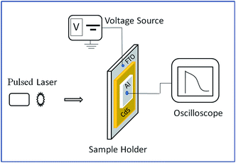
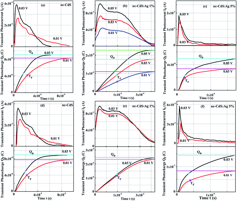
Melt quenching technique was used for the preparation of undoped and Ag doped CdS material (at two different Ag concentrations i.e. Ag 1% and Ag 5% by atomic percentage). Component elements (5 N pure) were sealed in quartz ampoules after weighing the constituent elements according to their atomic percentages. The vacuum of 2 × 10⁻⁵ mbar was maintained while quartz ampoules sealing. Sealed ampoules were kept inside the furnace where the temperature is increased up to 1200 °C at a heating rate of 2–3 °C min−1. The ampoules were kept inside the furnace at the highest melting point temperature of the component elements for 24 h to make homogeneous melt. The quenching of the sealed ampoules was carried out in ice cold water. Thermal vacuum evaporation [vacuum coating unit HINDHIVAC, Model: VS-65D] was used to deposit the thin films on well degassed Corning 7059 glass substrate using inert gas (Ar) condensation (IGC) technique. The whole process was carried out at a base pressure of 2 × 10⁻⁵ mbar and at room temperature. To obtain the thermodynamic equilibrium, thin films were kept in dark deposition chamber for 24 h before taking the measurements. The structural parameters of nc-CdS samples were estimated by X-Ray Diffraction (XRD) using a Spinner 3064 XPERT-PRO X-ray diffractometer (CuKα = 1.54056 Å) at a scanning speed of 0.02° s−1 in the 2θ range from 10° to 80°. X-ray Photoelectron Spectroscopy (XPS) experiments were performed using monochromatized Al Kα (1486.7 eV) radiation source in multiprobe surface analysis system (Omicron, Germany) operating at a base pressure of 5 × 10⁻¹¹ Torr. The high-resolution spectra was recorded using a hemispherical analyzer operating at a pass energy of 20 eV with 7 channeltron system. An energy correction was applied to account for sample charging on the C (1s) peak at a binding energy of 284.8 eV. Energy Dispersive Analysis of X-ray (EDAX) coupled with SU-8000 Scanning Electron Microscope (FE-SEM) (Model: HI-0876-0003) was used to determine the composition of thin films and to study the FE-SEM graphs. Prior to FE-SEM analysis, a thin layer of platinum (Pt) was deposited on thin films. Maltese cross-like indium (In) electrodes (diagonally separated by 0.25 cm each) were deposited by vapor deposition technique for Hall measurements.For TOF measurements, transparent fluorinated tin oxide (FTO) glass substrates were used for thin film deposition. Al layer was deposited by thermal vacuum evaporation on top of pre-deposited thin films. As a light source, Nd-YAG laser working at the wavelength (λ) ∼1064 nm, pulse width ∼10 ns and power ∼10 mJ was used. For signal-to-noise ratio improvement, the sample was kept in a specially designed metallic sample holder.23 Digital phosphor oscilloscope (Model: Tektronix DPO 4054; interface software Tekvisa) was utilized to record the electric current produced in the presence of an applied electric field. Fig. 1 shows the TOF apparatus used for the drift mobility measurements.
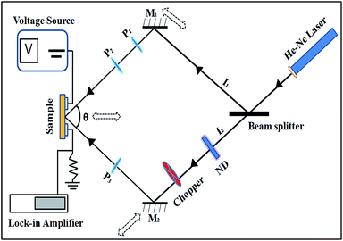
SSPC measurements were performed on all the samples under a vacuum of 10−3 mbar. A continuous and monochromatic blue laser having the wavelength of 405 nm was used to illuminate the sample. Experimental setup for the SSPG technique is shown in Fig. 2. A He–Ne laser (532 nm) was used and chopped (AMETEK Model 197) at the frequency of 80 Hz to measure the small-signal photocurrent between the coplanar electrodes (gap = 0.8 mm) of undoped and doped nc-CdS samples with lock-in-amplifier (EG & G DSO 7265). Two coherent beams of intensities I1 and I2 were produced by splitting the polarizing laser beam with the help of beam splitter. The coherent beams intensity ratio (I2/I1) is reduced to 10% by using neutral density (ND) filter. These two laser beams are made to coincide on the sample by two mirrors (M1&M2) with an angle symmetric around the normal to the sample surface. The plane of polarization was changed by placing a set of the polarizer in the path of two beams. In case of parallel polarization, the two beams produced a grating profile of light intensity on sample surface after interference. On the other hand, in case of perpendicular polarization (in crossed position), uniform illumination was produced on the sample surface. The sample holder and mirrors were moved toward or away (shown by dotted double faced arrows in Fig. 2) to the beam splitter to change the grating period (Λ).
Results and discussion
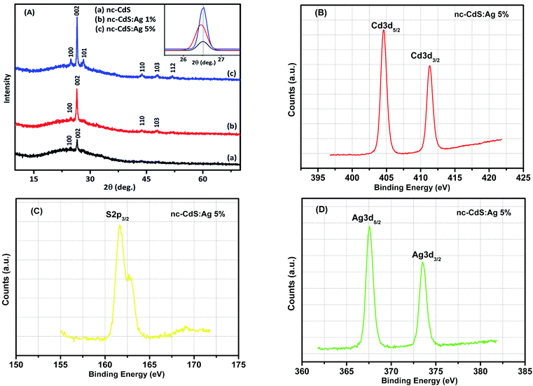
X-ray diffraction is performed to study the effect of doping on the crystallization behavior of the investigated thin films. Fig. 3 shows the XRD patterns of undoped nc-CdS and Ag-doped nc-CdS thin films. The polycrystalline nature of thin films with preferential growth of the crystal along (002) plane is observed. The various diffraction peaks corresponding to the hexagonal phase of CdS crystal are indexed using powder diffraction standard data (JCPDS card no. 06-0314). Also, it is observed that the preferred orientation of CdS thin films are along (002) with some other new orientations such as (101), (110), (103) and (112) are seen in XRD pattern of doped films. No extra peaks corresponding to Ag2S or other phases are found. From Fig. 3, we have also observed a systematic increase in the intensity of peaks with an increase in Ag doping. At lower Ag (∼1%) doping, Ag atoms might be replacing Cd atoms in the lattice substitutionally which in turn enhanced the intensity than that of the undoped CdS thin film. At higher Ag (∼5%) doping, Ag might be starting to enter the lattice both interstitially and substitutionally which causes the intensity to increase again. Muthusamy et al.24 also observed the increase in the intensity of XRD peaks of Al doped CdS films prepared by chemical bath deposition method at 80 °C. From the inset of Fig. 3(A), it is seen that the peak position is shifted to the lower angle at low Ag (∼1%) doping and while it is shifted to the higher angle at high Ag (∼5%) doping than the undoped CdS. FWHM corresponding to most intense peak (002) increases with lower Ag concentration and decreases with higher Ag concentration (tabulated in Table 1). The change in peak position and FWHM along (002) plane indicate that the microstructure, the quality of the crystal and the lattice parameters are affected by Ag-doping.| Sample | d (nm) | XRD | SEM | Hall measurements | TOF | |||||||
|---|---|---|---|---|---|---|---|---|---|---|---|---|
| β (rad) | D (nm) | ε (Lines−2 m−4) | Grain size (nm) | Hall coefficient (Ω cm G−1) | n (cm−3) | Bias (V) | For electrons | For holes | ||||
| Tr (s) | µe (cm2 V−1 s−1) | Tr (s) | µh (cm2 V−1 s−1) | |||||||||
| nc-CdS | 272 | 5.53 × 10⁻³ | 27 | 13.46 × 10⁻⁴ | 69 | −2.3 × 10⁴ | 2.63 × 10¹⁴ | 0.03 | 1.6 × 10⁻⁵ | 7.76 × 10⁻⁴ | 1.9 × 10⁻⁵ | 6.48 × 10⁻⁴ |
| nc-CdS:Ag 1% | 351 | 6.07 × 10⁻³ | 25 | 14.77 × 10⁻⁴ | 63 | −3.4 × 10⁴ | 1.78 × 10¹⁴ | 0.03 | 1.43 × 10⁻⁴ | 1.44 × 10⁻⁴ | 1.46 × 10⁻⁴ | 1.4 × 10⁻⁴ |
| nc-CdS:Ag 5% | 515 | 4.11 × 10⁻³ | 36 | 10.01 × 10⁻⁴ | 88 | −5.9 × 10³ | 1.05 × 10¹⁵ | 0.03 | 2 × 10⁻⁶ | 2.21 × 10⁻² | 3.6 × 10⁻⁶ | 1.22 × 10⁻² |
The crystallite size (D) corresponding to the predominating peak (002) is calculated by using Debye Scherrer's formula:25
 | (1) |
 | (2) |
![[thin space (1/6-em)]](https://www.rsc.org/images/entities/char_2009.gif) sin
sin![[thin space (1/6-em)]](https://www.rsc.org/images/entities/char_2009.gif) θ. Calculated lattice parameter ‘c’ for nc-CdS, nc-CdS:Ag 1% and nc-CdS:Ag 5% thin film is found to be 6.727 Å, 6.736 Å and 6.718 Å, respectively. The observed value of c-axis lattice parameter for each sample is greater than bulk CdS lattice parameter (c = 6.713 Å). This indicates that the undoped and Ag doped CdS thin films are under tensile strain along the (002) plane parallel to the substrate surface. The micro-strain shows the same trend as observed in c-axis lattice parameter. From the observed values of c-axis lattice parameter, it is noticed that the CdS lattice expands for low Ag (∼1%) concentration than the undoped CdS lattice. The observed lattice expansion for low Ag doping indicates the substitution of Cd sites by Ag atoms as the ionic radius of Ag+ (1.26 Å) is greater than that of Cd2+ (0.97 Å).27 Due to this, the strain in the CdS thin films increases at lower Ag doping; it results in decrease in crystallite size. However, the lattice constant and strain decreases at high Ag doping that could be due to the increase of number of interstitial Ag+ ions; it results in increase in crystallite size.
θ. Calculated lattice parameter ‘c’ for nc-CdS, nc-CdS:Ag 1% and nc-CdS:Ag 5% thin film is found to be 6.727 Å, 6.736 Å and 6.718 Å, respectively. The observed value of c-axis lattice parameter for each sample is greater than bulk CdS lattice parameter (c = 6.713 Å). This indicates that the undoped and Ag doped CdS thin films are under tensile strain along the (002) plane parallel to the substrate surface. The micro-strain shows the same trend as observed in c-axis lattice parameter. From the observed values of c-axis lattice parameter, it is noticed that the CdS lattice expands for low Ag (∼1%) concentration than the undoped CdS lattice. The observed lattice expansion for low Ag doping indicates the substitution of Cd sites by Ag atoms as the ionic radius of Ag+ (1.26 Å) is greater than that of Cd2+ (0.97 Å).27 Due to this, the strain in the CdS thin films increases at lower Ag doping; it results in decrease in crystallite size. However, the lattice constant and strain decreases at high Ag doping that could be due to the increase of number of interstitial Ag+ ions; it results in increase in crystallite size.
To investigate the bonding state and the chemical composition, we performed XPS measurements on the 5% Ag doped nc-CdS thin film. The Cd 3d, S 2p, and Ag 3d core level emissions are presented in Fig. 3(B–D), respectively. According to the results, the binding energy values of Cd 3d5/2 and 3d3/2 are 404.6 eV and 411.35 eV respectively with a separation of 6.75 eV. The binding energy value of S 2p3/2 is 161.65 eV. The cadmium 3d5/2 peak at 404.6 eV and sulfur 2p3/2 peak at 161.65 eV confirmed the formation of CdS and these peak positions are attributed to Cd2+ and S2− species, respectively.28 The binding energy position of the additional doublets (3d3/2) in the Cd 3d spectrum is related to Cd2+ species. As per the obtained XPS results, the Ag 3d5/2 and Ag 3d3/2 peaks are centered at 367.55 eV and 373.5 eV, respectively, indicating that the doped silver in our sample is in Ag+ state.29 Therefore, the Ag+ either form Ag2S compound or is incorporated in the CdS main structure. But the XRD analysis rules out the presence Ag2S phase in thin films. Thus, it is strongly evidenced that the silver is successfully inserted in the Cd–S matrix and occupied the Cd2+ site or occupied the interstitial site in the CdS lattice. The calculated atomic concentration of Cd, S and Ag is 47.11%, 48.52% and 4.36% respectively. The atomic concentration result obtained is found comparable to the result from the EDAX.
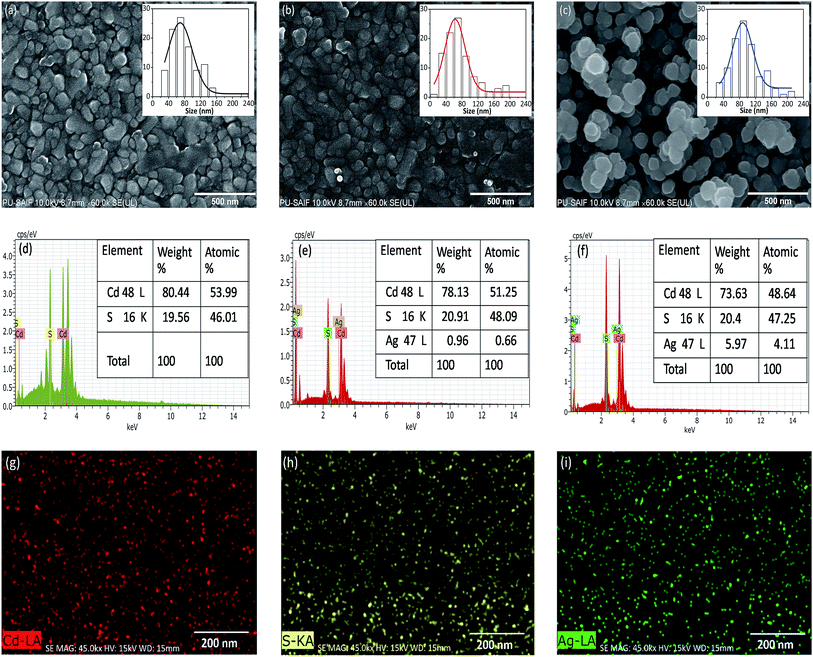
FE-SEM is a favorable technique for surface morphological analysis of thin films and it provides the beneficial information about the size and shape of the grains. Fig. 4 (panel (a, b and c)) presents FE-SEM micrographs of nc-CdS, nc-CdS:Ag 1% and nc-CdS:Ag 5% films, respectively. These images reveal that the films are homogeneous, free from cracks or holes, and well covered the substrate surface. The undoped (panel a) and Ag 1% doped (panel b) nc-CdS films show grains of irregular in shape and size. As Ag concentration increases to 5%, size of the grains increases and shape becomes spherical. The insets in Fig. 4 parts a–c show frequency of grains with size histograms. It is seen from Fig. 4 part a–c (SEM images and insets) that Ag doping not only modify the surface morphology of the nc-CdS films but also have significant effect on the grain size. The observed mean grain size is listed in Table 1. These observations can be related to our X-ray diffraction data, where the crystallite size also shows similar variations as found in mean grain size. The SEM shows higher values of grain size than XRD. XRD provides the coherent domain size which could be less than the size calculated from SEM image because X-ray visualizes a part of grain separated by defect as a coherent domain and treat it as a single crystallite. However, in SEM, we visualize complete grain of higher size. Nazir et al.8 and Ma et al.30 also observed the increase in grain size of Ag doped CdS films prepared by close spaced sublimation (CSS) and ultrasound-assisted microwave synthesis methods, respectively.
The purity and the precise composition of undoped and Ag doped nc-CdS thin films determined by EDAX study reveal the presence of Cd, S and Ag as elementary constituents. EDAX spectra of the nc-CdS, two doped systems nc-CdS:Ag 1% and nc-CdS:Ag 5% is shown in Fig. 4(d–f). Quantitative atomic percentage of the compositional elements (Cd, S and Ag) present in thin films are given as inset of Fig. 4 panels (d–f). From the XRD and EDAX results, it is clear that Ag is properly inserted in Cd–S matrix. The Cd/S ratio for nc-CdS, nc-CdS:Ag 1% and nc-CdS:Ag 5% sample is 1.173, 1.065 and 1.029 respectively. The change in this ratio from nc-CdS to 1% doping indicates that a large number of Ag atoms replacing Cd atoms substitutionally in CdS lattice. The Cd/S ratio changes slightly for 1% to 5% doping. It indicates that Ag atoms enter at interstitial sites more than substitution sites for high doping. The EDAX spectra show that the atomic% is slightly lower to their nominal stoichiometry.
Hall experiment is carried out on nc-CdS, nc-CdS:Ag 1% and nc-CdS:Ag 5% thin films to determine the concentration of charge carriers and carrier type at room temperature. The relation between Hall coefficient (RH) and Hall voltage (VH) is given as:31
 | (3) |
 | (4) |
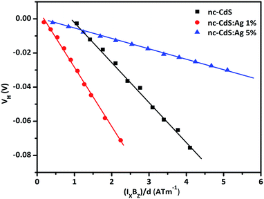 | ||
| Fig. 5 Variation of Hall voltage (VH) versus (IXBZ/d) for nc-CdS, nc-CdS:Ag 1% and nc-CdS:Ag 5% thin films. | ||
At low Ag doping, comparatively large numbers of Ag+ ions replace Cd2+ ions substitutionally in the CdS lattice. In this case, Ag acts as an acceptor because it provides an extra hole due to its deficiency in valence electrons. As a result of this, the observed carrier concentration decreases at low Ag doping than undoped nc-CdS. At high Ag doping, comparatively large numbers of Ag atoms occupy interstitial sites in CdS lattice. In this case, Ag acts as a donor and as a result, the electrons concentration increases at high Ag doping. These results are well supported by XRD and EDAX studies.
The main aim of the TOF transient photoconductivity analysis is to find out the carrier drift mobility by calculating the transit time (Tr). The transit time is the time taken by charge carriers created at one end of the sample to reach the other end under the effect of a constant applied electric potential, V. For this experiment, the sandwiched electrode configuration was used with at least one of the contacts to be semi-transparent for a large free-carrier generation. As the semi-transparent contact permits large free carrier generation by using a short and strongly absorbed laser pulse. The incident laser pulse generates a thin sheet of electron–hole pairs adjacent to the contact. The electrons and holes are driven towards the respective electrodes dependent upon the sign of applied electric field. The absorption depth of the optical excitation should be small compared to the film thickness and the optical pulse duration should be short compared to the Tr of the charge carriers.43 There are two popular methods for determining Tr. First, one analyzes the photocurrent decay over time. A drop or mostly a kink in the curve marks the Tr. Second, one integrates the photocurrent and measures the collected charge over time. Then, the time during which half of the total charge is collected is the Tr.44 The mobility, µ, can be directly estimated from the Tr as:45,46
 | (5) |
The observed values of µe and µh are low as compared to bulk mobility values for CdS (µe = 300 cm2 V−1 s−1, µh = 50 cm2 V−1 s−1). Tomakin et al.48 reported the observation of Hall effect with electron mobility ∼10−3 cm2 V−1 s−1 in CdS films prepared by thermal evaporation. Shikalgar et al.49 reported the electron mobility of chemically deposited Li doped CdS films ∼10−2 cm2 V−1 s−1 and is comparable with Ag 5% sample. There are a number of factors on which the variation in mobility of charge carriers in semiconductor thin films depend such as carrier concentration, electrostatic fluctuations due to charged defects, dislocations, a chemical disorder of vacancies, interstitials, substitutionals and grain size. The grain boundary potential barrier varies inversely with the carrier concentration. At higher carrier concentration, the grain boundary potential decreases. As a result, the carrier mobility of the film increases.50 Hall measurements show that the carrier concentration decreases for 1% Ag doping and increases for 5% Ag doping, hence the mobility decreases for low doping and increases for high doping. If the mobility of charge carriers is correlated with dislocation and strain in thin films then the variation in mobility can be explained of the basis of trap-limited band motion.51 The dislocations, strain, defects etc. present in the film form trapping states in the band gap. The transport of a carrier through extended states is repetitively disturbed by trapping in trapped states with later re-emission into the extended states after some time disbursed in traps. Drift mobility of these carriers is decreased proportionally to the time spent in traps. The trap-limited band motion of carriers can be explained in another way. After trapping mobile carriers, their mobility decreases because the traps are now electrical charged which create a potential energy barrier thus obstructing the motion of charge carriers.50 XRD results show that the strain and dislocation in 1% doping is higher and in 5% doping is lower than the undoped CdS film. Therefore the mobility of 1% doped film is reduced and for 5% doped film enhanced. If the mobility of charge carriers is correlated with nanocrystal size, then the variation in mobility can be explained on the base of nearest-neighbor-hopping (NNH) model.52 The NNH model describes charge transport as progressive hopping between the neighboring localized states. To describe the size dependent mobility of charge carriers, we must study two possibilities. Firstly, as the nanocrystal size increases, it is realistic that the electrons traveling via NNH across nanocrystal assemblies will cross a channel of fixed length in fewer hops. This concludes that the nanocrystalline films constructed from larger particles will exhibit greater mobility. Secondly, for the size dependence of mobility includes inhomogeneities in the locations of the charge energy levels. The charge carrier hops via electronic states having a different distribution of energy states due to the variation in nanocrystal size. Nanocrystalline thin films with narrower energy distribution have stronger inter particle coupling than the thin films having broader energy distribution. Stronger coupling in narrow energy distribution leads to higher values of mobility.53 XRD and SEM study show that the nc-CdS:Ag 5% films have a larger particle size as compare to nc-CdS films, so having high values of mobility of charge carriers. On the other hand, nc-CdS:Ag 1% films have a smaller particle size, hence having low values of mobility of charge carriers. Mondal et al.54 also observed an increment in electron mobility due to grain size growth in polycrystalline CdS films. The higher carrier concentration, larger grain size, lower strain and lower dislocations are the favorable factors for enhancing the mobility of charge carriers over two orders of magnitude in 5% Ag doped sample than undoped nc-CdS. The series resistance of the cells is related to carrier mobility inversely, higher carrier mobilities are desirable in a solar cell or photovoltaic applications. So the nc-CdS:Ag 5% thin films can be used in these applications.
Intensity dependent steady state photoconductivity (σPh) measurements have been performed on undoped and Ag doped nc-CdS thin films for getting information regarding the recombination process. Fig. 7 shows the variation of ln![[thin space (1/6-em)]](https://www.rsc.org/images/entities/char_2009.gif) IPh versus ln
IPh versus ln![[thin space (1/6-em)]](https://www.rsc.org/images/entities/char_2009.gif) F. As seen from figure, linear curves for all the samples indicate that σPh follows a power law i.e.
F. As seen from figure, linear curves for all the samples indicate that σPh follows a power law i.e.
| σPh ∝ Fγ | (6) |
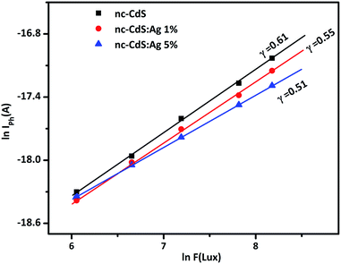 | ||
| Fig. 7 The intensity dependence of photoconductivity for nc-CdS, nc-CdS:Ag 1% and nc-CdS:Ag 5% thin films. | ||
| Sample | α × 104 (cm)−1 | γ | G × 1020 (cm−3 s−1) | (µτ)e × 10−7 (cm2 V−1) | L (nm) | LBalberg (nm) | Φ | (µτ)h × 10−10 (cm2 V−1) | b × 103 | τe (ms) | τh (µs) |
|---|---|---|---|---|---|---|---|---|---|---|---|
| nc-CdS | 2.3 | 0.61 | 4.63 | 4.76 | 43 | 41 | 0.84 | 3.57 | 1.33 | 0.61 | 0.55 |
| nc-CdS:Ag 1% | 2 | 0.55 | 2.42 | 6.40 | 41 | 38 | 0.78 | 3.24 | 1.97 | 4.44 | 2.31 |
| nc-CdS:Ag 5% | 3.4 | 0.51 | 4.30 | 47.43 | 53 | 55 | 0.99 | 5.42 | 8.57 | 0.21 | 0.04 |
µτ (cm2 V−1) represents the average length a carrier moves per unit field. For charge collecting devices, it is a significant figure of merit and is directly proportional to the conversion efficiency17 and quantum yield15 in photovoltaic devices and photodetectors, respectively. The higher µτ increases the diffusion length leading to an enhanced short-circuit current in the cell; higher charge carrier mobilities are required in these applications. For investigation of the majority and minority carrier mobility–lifetime product in undoped and Ag doped nc-CdS thin films, the SSPC and SSPG techniques are used.
The temperature dependent steady state photoconductivity is measured for nc-CdS, nc-CdS:Ag 1% and nc-CdS:Ag 5% samples in the temperature range from 200–340 K. The SSPC is dominated by the majority carrier transport. Hall measurements show that all films are n-type in nature i.e. electrons are the majority carriers in these films. From the steady state photoconductivity, the majority carrier (electrons) mobility–lifetime products can be evaluated by using the relation:56
 | (7) |
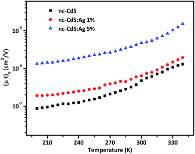 | ||
| Fig. 8 Temperature dependence of the majority carriers mobility–lifetime product for nc-CdS, nc-CdS:Ag 1% and nc-CdS:Ag 5% thin films. | ||
In SSPG technique two monochromatic plane laser beams of wavelength λ are illuminating the same area of the sample, making an angle θ between them as shown in Fig. 2. If the plane of polarization of two beams is in the same plane, an interference pattern formed inside the sample with grating period Λ given by the equation:19
 | (8) |
The ratio of the ac photocurrents with a grating (U∥) and without grating (U⊥) is defined by β. The relationship between β and Λ is given as:20
 | (9) |
 | (10) |
 | (11) |
(i) To confirm that the diffusion prevails over drift, the applied biasing voltage should be in Ohmic region of I–V curve and the β parameter should be independent of the applied voltage. The curves for the photocurrent with varying applied voltage are found to be symmetric and linear up to 100 V, indicating the Ohmic behavior of contacts. The electric field dependence of β parameter for all samples has been plotted in the inset of Fig. 9. Even though contacts are Ohmic for the electric fields of up to 1250 V cm−1 for I–V measurements, the β parameter values are independent of the electric fields only up to 125 V cm−1, thereafter they become field dependent for higher electric fields and the transport is not diffusion controlled any more. For each sample, measurements of the β parameter for different grating period Λ are carried out in low electric field 100 V cm−1, where the β parameter values are constant and satisfy the applied electric field condition E ≤ Ec, where Ec is the nominal critical electric field given by Ec = (kBT/e) (1/L).59
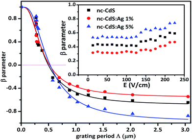 | ||
| Fig. 9 Typical variation of β versus grating period Λ for nc-CdS, nc-CdS:Ag 1% and nc-CdS:Ag 5%. The symbols represent the experimentally measured values and the full lines are the fits to eqn (6). Inset show the electrical field (E) dependence of experimental β-values for nc-CdS, nc-CdS:Ag 1% and nc-CdS:Ag 5% thin films at 300 K. | ||
(ii) The essential condition for the material to be in lifetime regime, the dielectric relaxation time τdiel should be much smaller than the common carrier recombination lifetime τ. Dielectric relaxation time is given by τdiel = ε0ε/σPh. Here ε0 is 8.85 × 10⁻¹⁴ F cm−1 and ε is the dielectric constant of the material. Estimated value of ε for nc-CdS thin film from the transmission data is 9.37. The common carrier recombination lifetime is given as, τ = (τe × τh)/(τe + τh) and has been calculated by using the values of τe and τh which are listed in Table 2. The ratio τ/τdiel has been calculated and it is found to be greater than unity for all samples; therefore the necessary condition for ambipolar transport in the lifetime regime is fulfilled.60,61
(iii) For accurate determination of diffusion length L, the surface recombination effects must be considered. For all the studied samples, the effect of surface recombination is small as L ≪ 1/α, and hence, it can be neglected while calculating the L values.19
Fig. 9 shows the experimental results for the β parameter versus the Λ for nc-CdS, nc-CdS:Ag 1% and nc-CdS:Ag 5% thin films. The β values change strongly for all the samples and become negative for the grating period higher than 0.5 µm. The variation in β parameter is not only controlled by diffusion length L but also the grating quality parameter Φ as defined in eqn (9).62 For this reason, parameters, L and Φ are obtained simultaneously using the nonlinear fit of eqn (9) to experimental data. Best fit results of β are shown in Fig. 9 as full lines. As theoretically expected, for the lower grating period values (Λ < L), the grating disappears and the β parameter approaches to unity. The calculated values of diffusion length L and Φ are listed in Table 2 for undoped and silver doped nc-CdS samples.
The value of diffusion length is also determined from the variation of Λ−2 versus , known as the Belberg's plots.63 Fig. 10 shows the Belberg plots for our samples obtained from the experimental β values at different grating period Λ. A straight line best fit to data points using eqn (10) for each sample confirms that the measured length for each case is ambipolar diffusion length.64 Calculated values of diffusion length LBelberg from the intercept of the Belberg plot are listed in Table 2. The calculated values of diffusion length L with best fit of data points of Fig. 9 to eqn (9) and from the intercept of Belberg plot show nearly similar results. The fine agreement between the two calculations is good indicator that the measurements are reliable even for the short diffusion length. The estimated value of (µτ)e product, increases slightly for low Ag doping and it increases a order of magnitude for higher Ag doping. The increase in (µτ)e product upon doping is linked with the shift of the Fermi level position. The parameter b [=(µτ)e/(µτ)h] defined as the ratio of the mobility–lifetime product of holes and electrons is taken as a measure of the Fermi level position.15,65 The b parameter increases after Ag doping indicating that the Fermi level shifts toward the conduction band (Table 2). The density of centers that seize majority carriers is significantly reduced due to the Fermi level shift caused by the change in thermal occupation. In case the Fermi level is near to conduction band, most of the defects would be thermally occupied by electrons and inaccessible to excess electrons, thus leading to a large electron lifetime and the large mobility–lifetime product.66 The diffusion length L values obtained from the best fits to data of Fig. 9 are used to calculate the minority carrier (hole) mobility–lifetime products using the Einstein relation (11). The calculated values of (µτ)h are shown in Table 2. It is clearly seen that majority carrier (µτ)e products are higher than the minority carrier (µτ)h products, for all undoped and Ag doped nc-CdS thin films, indicating electron dominated transport. The calculated values of diffusion length L and (µτ)h for nc-CdS:Ag 1% is slightly less than nc-CdS sample and they increase for nc-CdS:Ag 5% sample. From the calculated values of (µτ)h product, it is clear that the (µτ)h product is not so much affected by the Fermi level shift, but its values vary according to the variation in grain size as shown in XRD and SEM results. Generally, the grain boundaries contribute allowed energy levels in the semiconductor band gap and act as efficient recombination centers for the minority charge carriers. For minority carrier devices such as photovoltaic cells, this effect is significant. It is predictable that during recombination at the grain boundaries, some of the photogenerated carriers to be lost. With increasing grain size, the efficiency of the device will enhance.67 The literature values of mobility–lifetime product for bulk CdS are 1.6 × 10⁻⁷ cm2 V−1 (ref. 68) and 6.2 × 10⁻⁸ cm2 V−1 (ref. 69) for electrons and holes, respectively. The measured value of (µτ)e product is slightly higher and of the same order for nc-CdS and nc-CdS:Ag 1% as the bulk value. For nc-CdS:Ag 5% sample, the measured value of (µτ)e product is higher up to an order of magnitude as compared to the bulk value. On the other hand, the measured (µτ)h product is lower than the bulk value by two orders of magnitude for all the samples. The bulk value of τe and τh for CdS is 0.5 ns and 1.2 ns, respectively (calculated by using bulk values of mobility and mobility–lifetime product of electrons and holes, respectively). For comparison, we evaluate the carrier recombination time by dividing the measured mobility–lifetime product by measured electrons and holes mobility from TOF technique in our samples. The calculated values of τe and τh are listed in Table 2. The carrier lifetime enhances significantly in our samples as compared to bulk CdS. In solar cells and photodetectors, a higher lifetime of the carriers minimizes the recombination and maximizes the charge collection, which is desirable.70
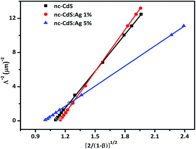 | ||
| Fig. 10 The Balberg plots of nc-CdS, nc-CdS:Ag 1% and nc-CdS:Ag 5% thin films obtained from β parameter and grating period Λ. The solid lines are the best fit to data using the eqn (10). | ||
Conclusions
Thin films of nc-CdS, nc-CdS:Ag 1% and nc-CdS:Ag 5% are prepared by thermal evaporation using IGC technique. The compositions of prepared samples have been studied using EDAX analysis. XRD and FE-SEM studies reveal that the silver doping strongly affects the structural morphology of the films and the average grain size decreases for low Ag doping concentration whereas it increases for high Ag doping concentration. We have presented a study for the evaluation of transport parameters like drift mobility for electrons and holes, mobility–lifetime product of charge carriers and recombination lifetime of carriers in undoped and Ag doped nc-CdS thin films using TOF, SSPC and SSPG techniques. We have fully applied all the required conditions of SSPG method to obtain reliably the ambipolar diffusion length L and hence (µτ)h product of minority carriers. The measured values of mobility and mobility–lifetime product for electrons are higher than holes in all the thin films. The bimolecular nature of recombination for photocurrent is dominating in all the samples. The calculated values of (µ)e and (µ)h using TOF technique decreases for low Ag doping and increases for high Ag doping in nc-CdS thin films. From SSPC, the observed (µτ)e product of majority carriers for the Ag doped films increase as compare to pure nc-CdS films. The diffusion length L and (µτ)h product of minority carriers shows the similar variation like mobility, decrease for low Ag doping and increase for high Ag doping in nc-CdS. We have observed that the recombination life-time of carriers enhanced significantly in doped and undoped nc-CdS as compare to bulk CdS. These studies suggest that the Ag doped and undoped nc-CdS thin films are promising candidate for charge-collecting devices including photovoltaics and photodetectors.Conflicts of interest
There are no conflicts of interest to declare.Acknowledgements
This work is financially supported by University Grant Commission (UGC) (Major Research Project: F. No. 42-781/2013(SR)), New Delhi. One of the authors (Baljinder Singh) wishes to thank University Grant Commission (UGC), India for providing Teacher Fellowship to complete Ph.D under the Scheme of ‘Faculty Development Programme’. The authors are thankful to the Dr Govind Gupta, Principal Scientist, CSIR-National Physical Laboratory (NPL), New Delhi-110012, India, for providing data of XPS.References
- J. S. Jie, W. J. Zhang, Y. Jiang and S. T. Lee, Appl. Phys. Lett., 2006, 89, 223117 CrossRef
.
- K. P. Bhandari, P. J. Roland, H. Mahabaduge, N. O. Haugen, C. R. Grice, S. Jeong, T. Dykstra, J. Gao and R. J. Ellingson, Sol. Energy Mater. Sol. Cells, 2013, 117, 476 CrossRef CAS
.
- D. Wu, Y. Jiang, Y. Zhang, Y. Yu, Z. Zhu, X. Lan, F. Li, C. Wu, L. Wang and L. Luo, J. Mater. Chem., 2012, 22, 23272 RSC
.
- K. M. Deng and L. Li, Adv. Mater., 2014, 26, 2619 CrossRef CAS PubMed
.
- Z. Lou, L. Li and G. Shen, Nanoscale, 2016, 8, 5219 RSC
.
- X. Ma, S. Guo, J. Shen, Y. Chen, C. Chen, L. Sun, X. Zhang and S. Ruan, RSC Adv., 2016, 6, 70907 RSC
.
- J. Kaur and S. K. Tripathi, J. Alloys Compd., 2015, 622, 953 CrossRef CAS
.
- A. Nazir, A. Toma, N. A. Shah, S. Panaro, S. Butt, R. R. Sagar, W. Raja, K. Rasool and A. Maqsood, J. Alloys Compd., 2014, 609, 40 CrossRef CAS
.
- D. Kim, Y. Park, M. Kim, Y. Choi, Y. S. Park and J. Lee, Mater. Res. Bull., 2015, 69, 78 CrossRef CAS
.
- S. Aksaya, M. Polatb, T. Ozera, S. Koseb and G. Gurbuzb, Appl. Surf. Sci., 2011, 257, 10072 CrossRef
.
- S. Kundu and H. Liang, Adv. Mater., 2008, 20, 826 CrossRef CAS
.
- S. Kundu, H. Lee and H. Liang, Inorg. Chem., 2009, 48, 121 CrossRef CAS PubMed
.
- J.-S. Ma, S. Das and C.-H. Lu, RSC Adv., 2016, 6, 107886 RSC
.
- S. M. Sze, Physics of Semiconductor Devices, Wiley, New York, 2nd edn, 1981 Search PubMed
.
- N. Beck, N. Wyrsch, C. Hof and A. Shah, J. Appl. Phys., 1996, 79, 9361 CrossRef CAS
.
- F. Galluzzi, J. Phys. D: Appl. Phys., 1985, 18, 685 CrossRef CAS
.
- D. Caputo, G. Cesare and M. Tucci, Sens. Actuators, A, 2001, 88, 139 CrossRef CAS
.
- G. F. Seynhaeve, R. P. Barclay, G. J. Adriaenssens and J. M. Marshall, Phys. Rev. B: Condens. Matter Mater. Phys., 1989, 39, 10196 CrossRef CAS
.
- D. Ritter, K. Weiser and E. Zeldov, J. Appl. Phys., 1987, 62, 4563 CrossRef CAS
.
- D. Ritter, E. Zeldov and K. Weiser, Appl. Phys. Lett., 1986, 49, 791 CrossRef CAS
.
- D. Ritter, K. Weiser and E. Zeldov, Phys. Rev. B: Condens. Matter Mater. Phys., 1988, 38, 8296 CrossRef
.
- R. I. Badran, J. Optoelectron. Adv. Mater., 2008, 10, 174 CAS
.
- B. Chen, C. Lee, S. Lee, P. Webb and Y. Chan, Jpn. J. Appl. Phys., 2000, 39, 1190 CrossRef CAS
.
- M. Muthusamy, S. Muthukumaran and M. Ashokkumar, Ceram. Int., 2014, 40, 10657 CrossRef CAS
.
- B. D. Culity, Elements of X-Ray
Diffraction, Addison-Wesley Reading, 1978, vol. 2 Search PubMed
.
- J. P. Enriquez and X. Mathew, Sol. Energy Mater. Sol. Cells, 2003, 76, 313 CrossRef CAS
.
- S. Huang, Y. Lin, J. Yang, X. Li, J. Zhang, J. Yu, H. Shi, W. Wang and Y. Yu, RSC Adv., 2013, 3, 20782 RSC
.
- Q. Wei, Y. Zhao, Q. Di, J. Liu, M. Xu, J. Liu and J. Zhang, J. Phys. Chem. C, 2017, 121, 6152 CAS
.
- M. Ristova and M. Ristov, Appl. Surf. Sci., 2001, 181, 68 CrossRef CAS
.
- J. Ma, G. Tai and W. Guo, Ultrason. Sonochem., 2010, 17, 534 CrossRef CAS PubMed
.
- C. Kittle, Introduction to Solid State Physics, 2005, vol. 8 Search PubMed
.
- N. G. Dhere, H. R. Moutinho and R. G. Dhere, J. Vac. Sci. Technol., A, 1987, 5, 1956 CAS
.
- M. Avinor and G. Meijer, J. Chem. Phys., 1960, 32, 1456 CrossRef CAS
.
- A. L. Robinson and R. H. Bube, J. Appl. Phys., 1971, 42, 5280 CrossRef CAS
.
- V. Swaminathan and L. C. Greene, J. Lumin., 1976, 14, 357 CrossRef CAS
.
- M. Inoue, J. Phys. Chem. Solids, 1979, 40, 857 CrossRef
.
- J. P. Chamonal, E. Molva, J. L. Pautrat and L. Revoil, J. Cryst. Growth, 1982, 59, 297 CrossRef CAS
.
- A. N. Georgobiani, U. A. Aminov, V. A. Dravin, L. S. Lepnev, I. D. Mullabaev, V. V. Ursaki and Z. P. Iljukhina, Nucl. Instrum. Methods Phys. Res., Sect. A, 1999, 426, 164 CrossRef CAS
.
- F. Sato, T. Kagawa, Y. Yodo and T. Iida, IEEE Nucl. Sci. Symp. Conf. Rec., 2004, 1–5, 3527 Search PubMed
.
- A. Sahu, M. S. Kang, A. Kompch, C. Notthoff, A. W. Wills, D. Deng, M. Winterer, C. D. Frisbie and D. J. Norris, Nano Lett., 2012, 12, 2587–2594 CrossRef CAS PubMed
.
- T. D. Dzhafarov, M. Serin, D. Oren, B. Sungu and M. S. Sadigov, J. Phys. D: Appl. Phys., 1999, 32, L5 CrossRef CAS
.
- R. Laiho, A. V. Lashkul, E. Lahderanta, D. D. Nedeoglo, N. D. Nedeoglo and M. A. Shakhov, Semicond. Sci. Technol., 2006, 21, 654 CrossRef
.
- I. H. Campbell and D. J. Smith, Appl. Phys. Lett., 1999, 74, 2809 CrossRef CAS
.
- U. Rau, D. Abou-Ras and T. Kirchartz, Advanced Characterization Techniques for thin film Solar Cells, 2011, ch. 9 Search PubMed
.
- Q. Long, S. A. Dinca, E. A. Schiff, M. Yu and J. Thei, Appl. Phys. Lett., 2014, 105, 042106 CrossRef
.
- N. Yazdani, D. Bozyigit, O. Yarema, M. Yarema and V. Wood, J. Phys. Chem. Lett., 2014, 5, 3522 CrossRef CAS PubMed
.
- C. Main and D. Nesheva, J. Optoelectron. Adv. Mater., 2001, 3, 655 CAS
.
- M. Tomakin, M. Altunbas, E. Bacaksiz and S. Celik, Thin Solid Films, 2012, 512, 2532 CrossRef
.
- A. G. Shikalgar and S. H. Pawar, Solid State Commun., 1979, 32, 361 CrossRef CAS
.
- J. Y. W. Seto, J. Appl. Phys., 1975, 46, 5247 CrossRef CAS
.
- J. M. Marshall, Rep. Prog. Phys., 1983, 46, 1235 CrossRef
.
- S. Baranovski, Charge Transport in Disordered Solids with Applications in Electronics, John Wiley & Sons, Chichester, 2006 Search PubMed
.
- M. S. Kang, A. Sahu, D. J. Norris and C. D. Frisbie, Nano Lett., 2010, 10, 3727 CrossRef CAS PubMed
.
- A. Mondal, T. K. Chaudhuri and P. Pramanik, Sol. Energy Mater., 1983, 7, 431 CrossRef CAS
.
- A. Rose, Concepts in Photoconductivity and Allied Problems, Interscience, New York, 1963 Search PubMed
.
- A. S. Al-Kabbi, K. Sharma, G. S. S. Saini and S. K. Tripathi, Phys. Scr., 2013, 87, 025604 CrossRef
.
- R. Bruggemann, J. Phys.: Conf. Ser., 2010, 253, 012081 CrossRef
.
- Y. Yang, J. Li, H. Wu, E. Oh and D. Yu, Nano Lett., 2012, 12, 5890 CrossRef CAS PubMed
.
- J. Hubin, E. Sauvain and A. Shah, IEEE Trans. Electron Devices, 1989, 36, 2789 CrossRef CAS
.
- R. I. Badran, J. Optoelectron. Adv. Mater., 2008, 19, 174 Search PubMed
.
- M. Niehus and R. Schwarz, Superlattices Microstruct., 2006, 40, 350 CrossRef CAS
.
- S. Okur, M. Gunes and O. Goktas, J. Mater. Sci.: Mater. Electron., 2004, 15, 187 CrossRef CAS
.
- I. Balberg, K. A. Epstein and D. Ritter, Appl. Phys. Lett., 1989, 54, 2461 CrossRef
.
- T. Toyama, M. Nishino, T. Kawabe, Y. Sobajima and H. Okamoto, J. Non-Cryst. Solids, 2008, 354, 2223 CrossRef CAS
.
- A. Shah, E. Sauvain, J. Hubin, C. Pipoz and C. Hof, Philos. Mag. B, 1997, 75, 925 CrossRef CAS
.
- R. Bruggemann and C. Main, Phys. Rev. B: Condens. Matter Mater. Phys., 1998, 57, 24 CrossRef
.
- B. G. Yacobi, Semiconductor Materials: An Introduction to basic principles, Kluwer Academic Publishers, 2006 Search PubMed
.
- C. Weber, U. Becker, R. Renner and C. Z. Klingshirn, Phys. B, 1988, 72, 379 CrossRef CAS
.
- R. B. Stephens, Phys. Rev. B: Condens. Matter Mater. Phys., 1984, 29, 3283 CrossRef CAS
.
- Y. Gu, J. P. Romankiewicz, J. K. David, J. L. Lensch and L. J. Lauhon, Nano Lett., 2006, 6, 5 CrossRef
.
| This journal is © The Royal Society of Chemistry 2017 |

