
 Open Access Article
 This Open Access Article is licensed under a
 Creative Commons Attribution 3.0 Unported Licence
Quantitative analysis of nanoscale electrical properties of CNT/PVDF nanocomposites by current sensing AFM†
V. Ozhukil Kollath a,
M. Arjmanda,
P. Egbertsb,
U. Sundararaja and
K. Karan*a
a,
M. Arjmanda,
P. Egbertsb,
U. Sundararaja and
K. Karan*a
aDepartment of Chemical & Petroleum Engineering, Schulich School of Engineering, University of Calgary, 2500 University Drive, NW, Calgary – T2N 1N4, Alberta, Canada. E-mail: kkaran@ucalgary.ca; Fax: +1 403 284 4852; Tel: +1 403 220 5754
bDepartment of Mechanical and Manufacturing Engineering, Schulich School of Engineering, University of Calgary, 40 Research Place, NW, Calgary – T2L 1Y6, Alberta, Canada
First published on 26th June 2017
Abstract
Quantitative current sensing atomic force microscopy (CS-AFM) is used to characterize the nanoscale electrical properties of carbon nanotube/polyvinylidene fluoride (CNT/PVDF) nanocomposites made with two different CNTs – undoped CNT and N-doped CNT. The conducting domains on the surface connected via a percolating pathway were mapped as a function of applied electrical potential. The conducting domain size and fractal analyses assigned an interconnected aggregate model to the percolating network with the low resistive conducting domain radii ranging from 140–400 nm. These measurements compared well with those determined from bulk measurements for both undoped and N-doped nanocomposites. Significant differences between conductivities determined by CS-AFM and bulk measurements were noted. This difference in conductivity was attributed to challenges in measuring low currents at low applied potential and current saturation issues at high applied potential. For 3.5 wt% undoped CNT/PVDF nanocomposite, the fractional surface area contributing to current increased from 20% at 1 V to 60% at 10 V highlighting the distinct ability to map the distribution of conducting domains with varying resistance, which was not possible to determine through bulk conductivity measurements.
Introduction
Conductive filler/polymeric nanocomposites (CFPNs) are attractive for a wide spectrum of applications, within electronics, aviation, thermoelectric, energy storage and transportation industries, resulting from their lightweight, flexible semi-transparent physical properties, and low cost of manufacture.1–4 High conductivity in CFPNs can be achieved at relatively low nanofiller concentrations provided that a percolating network of the nanofillers is achieved. Lowering the percolation threshold is a common goal for the manufacturing of CFPNs. The aggregation state of the fillers and the inter-aggregate connectivity are then the key factors in achieving low percolation threshold. Thus the filler–filler and filler–polymer interactions become important, in addition to the filler–polymer mixing process, for achieving low percolation threshold.5–9 As one may expect, the structural properties of the fillers, e.g. carbon nanotube (CNT), significantly affect all of the aforementioned interactions. For example, a recent study on bulk electrical properties of CNT/polyvinylidene fluoride (PVDF) nanocomposites revealed better electrical properties of undoped CNT/PVDF over the nitrogen-doped (N-doped) CNT/PVDF nanocomposites, where CNT dispersion state was an important factor in differentiating the performance of these nanocomposites.8 Although microscopic techniques such as optical and transmission electron microscopies can reveal the 2D nanoscopic dispersion state of the matrix from micron thin slices of the composites, they do not provide quantitative information on the connected network and the conducting domain size at the surface. Current sensing atomic force microscopy (CS-AFM), belonging to the broader class of scanning probe microscopy (SPM), can be applied to gain insight into the conductive properties of the types of composite materials discussed above. CS-AFM and other SPM methods such as electrostatic force microscopy (EFM), and Kelvin probe microscopy (KPM) are powerful tools for probing the surface and sub-surface electrical properties of CFPNs.One of the first studies to report the use of CS-AFM for characterizing electrical properties of carbon black/polymer system was that by Matsushige et al.10 Later, Carmona, Ravier et al. reported a series of experiments on similar system using conductive probe AFM (termed then as resiscope).11–13 More recent studies have reported semi-quantitative analysis of subsurface electrical properties in CFPNs using other modes of AFM.14–16 The CS-AFM technique offers the distinct advantage of mapping the conducting domains in CFPNs as well as identification of low- and high-resistance domains. In addition, quantitative analysis of current–voltage data allows the estimation of local conductivity and extraction of the percolation threshold.
In this work, we apply CS-AFM to study two polymer nanocomposites, N-doped CNT/PVDF and undoped CNT/PVDF, for which the bulk conductivity and the percolation behaviour have been recently reported by Arjmand and Sundararaj.8 In particular, we are interested in probing the uniformity of CNT dispersions by mapping the low-/high- current or resistance domains as well as to compare the percolation behavior from such nanoscopic measurements with previously reported bulk property measurements.8 In addition, the paper discusses the influence of AFM parameters on such measurements, a topic that is not well discussed in the literature.
Experimental details
Nanocomposite synthesis
The details of the CNT synthesis and fabrication of nanocomposite have been described in detail elsewhere.17 Briefly, the CNTs were grown by chemical vapour deposition (CVD) technique on alumina supported Fe-catalyst (Sasol Catalox Sba-200). Undoped CNTs were synthesized using ethane/hydrogen/argon (50/50/50 sccm) mixture, whereas to synthesize N-doped CNTs, hydrogen gas was substituted with ammonia gas. Ethane was employed as the source of carbon, ammonia was the source of nitrogen, and argon and hydrogen were used as gas carriers to keep the reactor free of oxygen during the synthesis process. The synthesis temperature, synthesis time, and catalyst mass were kept at 650 °C, 2 h, and 0.6 g, respectively.A semi-crystalline PVDF 11008/0001 was procured from 3M Canada. Synthesized CNTs were melt mixed with the PVDF matrix at 240 °C and 235 rpm using an APAM setup (Alberta Polymer Asymmetric Minimixer).18 The PVDF matrix was first masticated for 3 min and then CNTs were inserted into the mixing cup and dispersed in the PVDF matrix for an extra 14 min. The nanocomposites for both undoped and N-doped CNTs were prepared at various CNT loadings, i.e., 0.3, 0.5, 1.0, 2.0, 2.7 and 3.5 vol%. Then, the nanocomposites were moulded with a Carver compression moulder (Carver Inc., Wabash, IN, USA) at 220 °C under 38 MPa pressure for 10 min to make circular samples of 0.5 mm thickness. Selected samples were immersed in N,N-Dimethylformamide (DMF) (ACS grade, Fisher Scientific) for 3 min for surface etching.
CNT characterization
The synthesized N-doped CNTs were characterized for content and bonding type of nitrogen using X-ray photoelectron spectroscopy (XPS) analysis (Physical Electronics PHI VersaProbe 5000-XPS) employing a monochromatic Al source at 1486.6 eV and 49.3 W with a beam diameter of 200.0 μm. The morphology of synthesized CNTs was captured on a transmission electron microscope (TEM) (Tecnai TF20 G2 FEG-TEM (FEI, Hillsboro, Oregon, USA)), and the average length and diameter of CNTs were obtained for 100 individual ones via the ImageJ software.19 The thermal stability and purity of synthesized CNTs were tested using a Thermogravimetric Analyzer Q500 (TA instruments, New Castle, DE, USA). The samples were heated under air atmosphere (Praxair AI INDK) from room temperature to 900 °C at a ramp rate of 10 °C min−1. The samples were kept at 900 °C for 10 min before cooling.The electrical conductivity of CNT powders was measured using a specially designed instrument. About 40–50 mg of the CNTs in powder form was filled into a cylinder and compressed with a piston, and then the electrical resistance of the powder was measured using a Keithley 2001 electrometer. The powder conductivity was measured at 30 MPa. Further details about this procedure are provided elsewhere.20
Nanocomposite characterization
The micro-dispersion state of CNTs within the PVDF matrix was evaluated using optical microscopy on thin cuts (5 μm thickness) of the nanocomposites. Thin cuts were prepared with a Leica EM UC6 (Leica Biosystems, Germany) ultramicrotome at room temperature. An Olympus BX60 optical microscope (Olympus Corporation, Japan) equipped with an Olympus DP80 camera was employed to take images with dimensions of 600 × 800 μm2 for 15 different cuts. Analysis of the images was performed using the software Stream Motion (Olympus). The agglomerate area ratio (in %) was determined by dividing the spotted area of non-dispersed CNTs (with equivalent circle diameter > 5 μm) over the whole sample area (15 cuts, ca. 7.2 mm2). The relative transparency was quantified by dividing the transparency of the sample cut on microscopic glass slide/cover glass over the transparency of the glass slide/cover glass assembly without any sample. The relative transparency gives information about the dispersion state of CNTs in the size scale equal to or slightly larger than the wavelength of visible light (400–700 nm).Transmission electron microscopy (TEM) was employed to investigate the nano-dispersion state of CNTs (below the LM limit) within the PVDF matrix. Ultrathin sections of the samples (60 nm) were cut using an ultramicrotome EM UC6/FC6 setup with an ultrasonic diamond knife at room temperature. The sections were floated off water, and thereafter transferred on carbon-filmed TEM copper grids. TEM imaging of the microtomed layers was carried out on a Tecnai TF20 G2 FEG-TEM (FEI, Hillsboro, Oregon, USA) at 200 kV acceleration voltage.
Scanning electron microscopy (SEM; Zeiss Sigma VP FE-SEM) was used to obtain the surface morphology of CNT/PVDF network after surface etching.
Bulk electrical conductivity of nanocomposites
Bulk electrical conductivity measurements were performed using two different electrometers with 90 V as the applied voltage. For the nanocomposites with an electrical conductivity > 10−4 S m−1, the measurements were conducted using a Loresta GP resistivity meter (MCP-T610 model, Mitsubishi Chemical Co., Japan) connected with an ESP four-pin probe. In an ESP probe, the pin probes are in linear arrangement, where a known current is passed through the two outer probes and the resulting voltage is measured across the inner probes using a voltmeter, thus the effect of contact resistance is eliminated. For electrical conductivities < 10−4 S m−1, the measurements were carried out using a Keithley 6517A electrometer connected to a Keithley 8009 test fixture (Keithley instruments, USA).CS-AFM
All CS-AFM measurements were conducted using a Keysight's model 5500 (N9410S, Keysight Technologies Canada Inc., ON, Canada) beam-deflection AFM. In all CS-AFM measurements, topographic images were collected using contact mode. Normal forces were chosen to optimize the lateral resolution of the acquired images while insuring minimal damage to the sample by the shearing forces present between the apex of the AFM tip and the soft polymer surface of the sample. Conductive PtSi coated silicon force sensors (Nanosensors PtSi-CONT) were used in all CS-AFM measurements. For CS-AFM measurements, the built-in conductive AFM hardware of the Keysight 5500 AFM was utilized. This limited the maximum measurable current flow from the sample to the tip, or vice versa, to 1 nA. Resulting from this limitation, the applied bias to the sample was then adjusted to ensure that this maximal current value was not exceeded during a single AFM scan frame. Electrical contact to the samples was accomplished by fixing them to the sample stage with conducting carbon tape. Before CS-AFM measurements were conducted, continuity resistance from the external AFM connections was confirmed using a high precision multimeter (U1231A, Agilent). Bias is applied to the sample stage unless specified otherwise. A schematic of the setup is shown in Fig. 1.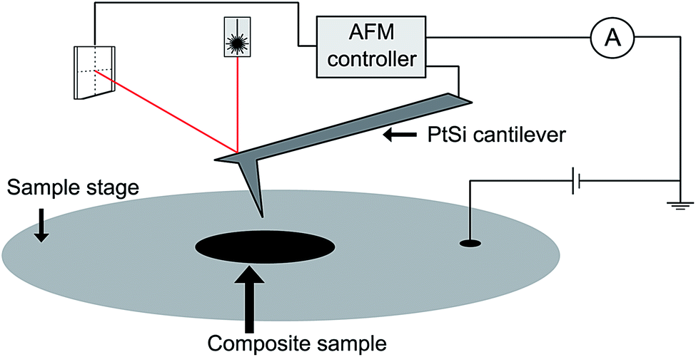 | ||
| Fig. 1 Diagram of the CS-AFM set up. The nanocomposite sample is fixed to a conducting sample stage and the bias voltage is applied to the stage. | ||
Standard scan size was set at 20 × 20 μm2 at 128 pts per line resolution. For quantitative analyses, 40 × 40 μm2 micrographs were recorded at 256 pts per line resolution. Image analyses were carried out using Gwyddion 2.42 and WSxM 5.0 softwares.21,22
Results and discussion
Morphological and physical properties of CNTs and nanocomposites
The morphology of synthesized CNTs and nanocomposites fabricated thereof has been reported earlier8 and some representative images are presented here. The physical properties of synthesized CNTs are reported in Table S1 (ESI†). The transmission electron micrographs (TEM) of the two CNTs are shown in Fig. 2(a and b) revealed that the diameter of N-doped CNTs are more than three times the diameter of undoped CNT. Undoped CNTs presented an open-channel structure with a well-ordered wall structure, whereas N-doped CNTs had a bamboo-like structure. Thus, at a given concentration or CNT loading, the total surface area provided by undoped CNTs will be much higher than that of N-doped CNTs. Furthermore, the powder electrical conductivity of undoped CNT was nearly 20% higher than N-doped CNTs (Table S1†) and the TGA results showed a higher thermal degradation for N-doped CNTs (see ESI† for more discussion).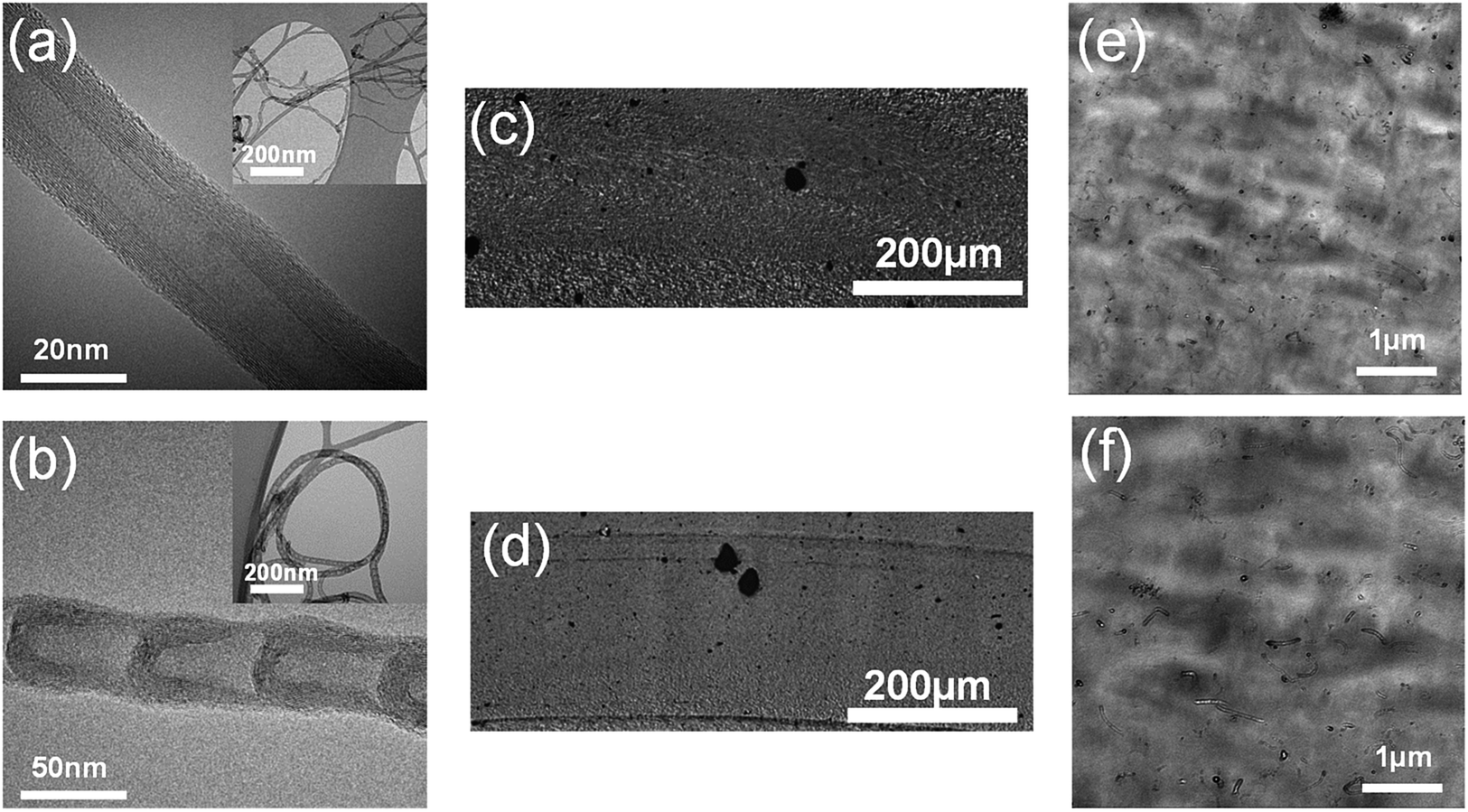 | ||
| Fig. 2 (a and b) Transmission electron micrographs of (a) undoped CNT and (b) N-doped CNT, with inset showing overall structure at lower magnification; (c and d) optical and (e and f) transmission electron micrographs of undoped CNT/PVDF (c and e) and N-doped CNT/PVDF (d and f) nanocomposites, showing the 2D dispersion state and agglomeration state. | ||
The optical and TEM images of undoped and N-doped nanocomposites with 2.0 vol% CNT loading is presented in Fig. 2(c–f). Optical microscopy reveals the presence of a few large agglomerates which are a portion of nanotubes that cannot be dispersed. This non-dispersed part was estimated using the agglomerate area ratio (agglomerates were defined as domains with equivalent circle diameter > 5 μm). Moreover, agglomerates with sizes equal to or slightly larger than the wavelength of visible light, ca. 400–700 nm, but smaller than visually identifiable agglomerates contribute to the darker appearance of the microtomed samples. Therefore, darker appearance of the microtomed samples signifies that more nanotubes are dispersed in this size range. The TEM micrographs also illuminate differences between the samples by showing the nano-dispersion state of CNTs. The agglomerate area ratio of undoped and N-doped nanocomposites was quantified to be 1.6% and 2.3%, respectively. The relative transparency of undoped and N-doped CNT/PVDF nanocomposites was determined to be 36% and 51%, respectively. These data confirm the micro-dispersion state of undoped CNTs was relatively better than N-doped CNTs within the PVDF matrix. TEM micrographs showed that both undoped and N-doped CNTs were well dispersed within the PVDF matrix without formation of any significant agglomerates.
From the results shown so far, four simplified probabilities of dispersion state in these nanocomposites may be thought of, as depicted in Fig. 3. Fig. 3(a) shows the nanofiller dispersion state below the percolation threshold. In this case, amount of nanofiller (e.g., CNT) is not enough to have an electric percolation through the nanocomposite. Fig. 3(b) shows the dispersion state above the percolation threshold, which allows electrical current through percolation pathways. Fig. 3(c) and (d) show the percolation dispersion state, but with nanofiller agglomeration. Such agglomerated dispersion states are more probable scenarios than the idealized state shown in Fig. 3(b). Although a combination of optical and electron microscopies gives some sense of the nanofiller dispersion state, poor phase contrast of TEM and optical technique still leads to ambiguous correlation of the dispersion state to the percolation properties of these nanocomposites. Thus, for a better understanding of the dispersion state and its relation to the nanoscopic electrical properties of CNT/PVDF nanocomposites requires information from a technique such as CS-AFM.
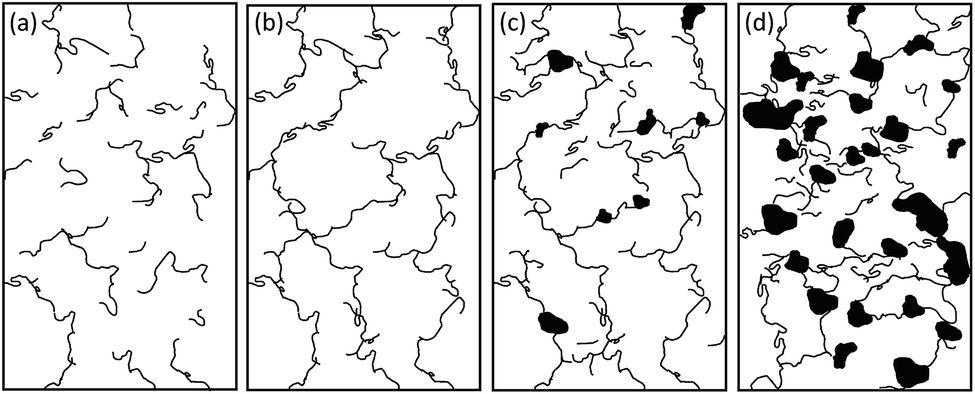 | ||
| Fig. 3 Possible CNT dispersion state in the nanocomposite. Nanofiller dispersion (a) below percolation threshold, (b) above percolation threshold, (c) above percolation threshold and with minimal agglomeration, (d) above percolation threshold and significant agglomeration. | ||
Effect of sample preparation on CS-AFM measurements of the nanocomposites
CS-AFM measurements of pure PVDF yielded no current spots (see ESI Fig. S1†) even at the highest bias voltage of 10 V, which is expected since the pure polymer is not conductive. However, we can clearly see current spots after undoped CNTs are added to PVDF. Fig. 4(a–c) shows the results of CS-AFM measurements on the unaltered samples (with CNT; before chemical etching) obtained from the molding process, all acquired under an applied bias of 4 V. Both topographic (Fig. 4(a)) and deflection (Fig. 4(b)) images show that the polymer surface is fairly flat and does not contain significant variations in topography resulting from the different material phases present in the nanocomposite. The current signal (Fig. 4(c)) does not show any significant variation over the entire surface, despite the fact that there is a significant change in conductivity between the polymer and filler phases. The absence of any significant variation in current over the surface is surmised to be due to the non-conducting polymer skin layer resulting from the molding process.23 In subsequent experiments, this skin layer was etched away by immersing the samples in N,N-dimethylformamide so that we could see the structure in the bulk. Fig. 4(d–f) shows the results of CS-AFM measurements on the etched samples. A significant increase in surface roughness can be visually observed in topographic (Fig. 4(d)) and deflection (Fig. 4(e)) images. The root mean square (RMS) roughness of the surface increased from 72 nm to 782 nm as a result of the etching process, which preferentially attacks the amorphous domains of the semi-crystalline PVDF sample, rather than its crystalline domains.24 The removal of the polymer skin layer that formed during the molding process is confirmed in the current image (Fig. 4(f)), where an almost bimodal distribution in current measured across the surface was recorded, indicating that conductive CNT is dispersed in the non-conductive PVDF in the sample bulk. Similar trend was observed for both the undoped and N-doped CNT/PVDF nanocomposites after etching the polymer skin layer. Representative scanning electron micrographs of the etched regions revealing CNT/PVDF network is shown in the ESI (Fig. S2†).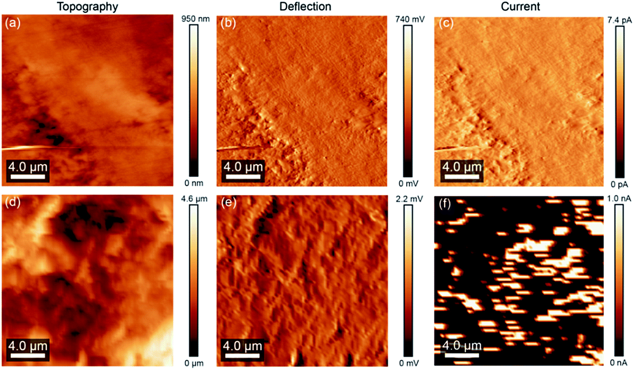 | ||
| Fig. 4 Micrographs of 1 vol% undoped CNT/PVDF nanocomposite biased at 4 V before (a–c) and after (d–f) chemical etching. | ||
Influence of AFM parameters on measured currents
For quantification of CS-AFM data, it is important to understand how the measured current can be influenced by the AFM scan parameters, excluding the sample preparation as the sole factor contributing to the measured nanoscopic conduction properties. For instance, it is well known that scan rates can affect the measured topographical features. A very high scan rate can give rise to edge overshoot and tip-sample convolution artefacts.25 Such effects may also influence the AFM measured currents. Although during current imaging, the conductive cantilever tip senses any current spots irrespective of the topography, diffusion effects can smear the spatial current profiles. Furthermore, the measured current response expectedly depends on the applied voltage. On one hand, at low applied voltage, the sensitivity of the potentiostat may not be sufficient to detect very small current through the highly resistive pathway connecting the tip and the bottom electrode. On the other hand, at higher voltages the low resistive pathways may yield currents that are high enough to saturate the response, i.e. the current levels may exceed the upper limit of measurable current range. Thus, we have examined the effect of these AFM parameters on the current response of the nanocomposite samples.We first examine the effect of scan speed on the measured current. As an example, the current response for N-doped CNT/PVDF nanocomposite sample scanned at four different scan rates – 0.1, 0.5, 0.9 and 2.0 lines s−1 are presented in Fig. 5(a–d). This corresponds to 4 × 10⁻⁶ m s−1, 2 × 10⁻⁵ m s−1, 3.6 × 10⁻⁵ m s−1 and 8 × 10⁻⁵ m s−1, respectively. Several noticeable differences in the responses with an increase in scan speed are evident. Both the peak value and the spatial broadening or diffusive effect in current are noticed when the scan speed is increased from 0.1 lines s−1 to 0.5 lines s−1 (Fig. 5(a) and (b)). Further increase in scan speed to 0.9 lines s−1 (Fig. 5(c)) shows a characteristic tail formation. The peak current is saturated at a value of 1 nA. This effect is more noticeable at scan speed 2 lines s−1 (Fig. 5(d)). Another interesting point to note is the directionality of the diffusive effect in trace (scan from left to right) and retrace (scan from right to left) data collected (Fig. 5(e) and (f)). This becomes evident at higher scan rates. These results point out that the scan speed should be carefully selected so as to not induce artefacts and introduce errors when the current images are quantified. From these experiments, the scan speed selected for the quantitative analysis in this study is 0.3 lines s−1.
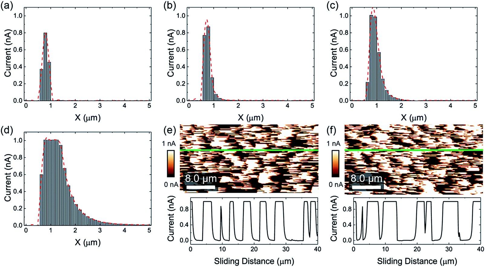 | ||
| Fig. 5 (a–d) Typical line profiles over high current region showing the diffusion effect with respect to scan rate. In (a)–(d) the grey histograms show the exact values of the pixels recorded in the image as the tip was scanned across the surface and the red dashed line shows a smoothened line profile of these pixel values. The scan rates are (a) 0.1, (b) 0.5, (c) 0.9, and (d) 2 lines s−1 respectively. (e and f) Forward and reverse current images acquired at 2 lines s−1 and an applied bias of 10 V. A green line marks the area where the line profile is shown below the current image. | ||
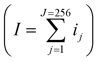
For quantification of any property from AFM measurements, the images are rasterized and each pixel is assigned a value. For higher accuracy, the pixel size should be smaller than the domain size of the property, e.g. current, being quantified. Similarly, consideration must be given to the tip size. In this study, for example, we used a conductive cantilever of nominal tip radius <30 nm. This means that for a micrograph created at 256 pts per line in a 40 × 40 μm2 scan area, the pixel size is approximately 150 nm. Due to the tip radius, the resolution will be limited below 10 × 10 μm2 scan area (at 256 pts per line). The higher scan area selected in this study was a compromise to get better statistical results to compare with bulk electrical properties.
For quantification, the measured current data may be represented as a histogram of events, e.g. number of pixels with a certain value of electrical current. Fig. 6 shows the current channel histogram for CNT/PVDF sample where a 10 V bias was applied. A bimodal distribution can be noted. The high current value of 1 nA arises from the saturation current. A significant number of events at current <40 pA can also be noted. The origin of these events can be traced to the inherent noise (<30 pA) associated with the setup as observed in separate experiments. A choice must be made whether to include the low current data in the analysis. The current in the noise range which is <30 pA can be neglected in the quantification protocol because the number of events at high current density is several orders of magnitude larger. On the other hand, these results highlight the limitation of the built-in potentiostat, which saturates the measured current value to 1 nA.
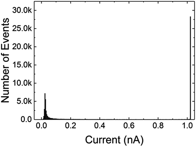 | ||
| Fig. 6 Typical histogram of a complete current scan area in an N-doped CNT/PVDF (3.5 vol%) sample biased at 10 V, showing a bimodal distribution. This particular histogram was calculated from Fig. 5(e). | ||
The current saturation can be resolved by external potentiostat and AFM modification. However, if the AFM system restricts the measurement to certain current values, e.g. 1 nA in this case, then the applied voltage should ideally be selected to have the current at any point in a scan area to stay lower than the maximum detectable current. Fig. 7 shows a current–voltage (I–V) curve for one of the undoped CNT/PVDF nanocomposite samples. The current value shown is the total current computed over the scanned area of 1600 μm2. It can be noted that, for this sample, above a threshold voltage of ∼0.6 V the current changes little with an increase in potential. This is not expected for a material with purely ohmic resistance and arises from the limitation of the potentiostat that limits the high current values to saturation current equals to 1 nA. On the other hand, at lower voltage, the I–V behaviour appears to follow a linear trend with the expected zero current response for zero applied voltage. Computation of a conductivity value from such measurements can thus be fraught with errors if the measurements are performed at voltage range where the results are skewed by saturated current values. On the other hand, if the percolating domains are to be estimated from the regions exhibiting current response, high voltage measurements are preferred because it ensures that the percolating domains belonging even to a highly resistive pathway will register measurable current response.
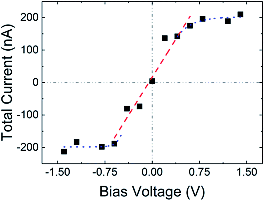 | ||
| Fig. 7 Representative I–V curve from 3.5 vol% undoped CNT/PVDF sample. Y-axis is the total current measured over 40 × 40 μm2 scan area. The blue dotted and red dashed line are for guidance only, but highlight the region influenced by the linear resistance of the composite (red dashed line) and saturation of the amplifier (blue dotted line). A grey dashed line demarks the values of 0 V and 0 nA. | ||
Mapping of conductive domains
CS-AFM measurements on a set of CNT/PVDF polymer nanocomposite films were carried out at a line scan rate of 0.3 lines s−1. As pointed out earlier, two different types of CNT fillers were studied: undoped CNT and N-doped CNT. Nanocomposites with undoped CNT showed a gradual increase in the number of current conducting paths, with an increase in bias voltage. Fig. 8 shows the topology and current maps for PVDF nanocomposite with 3.5 wt% undoped CNT. Fig. 8(a) and (b) show the evolution of current while the bias voltage ramped from 0–10 V. Qualitatively, one can easily detect the current saturation (1 nA) for bias voltages of 2 V and 10 V. At 0.1 V bias voltage, the current spots appeared are probably from the lowest resistance pathways in the percolation network and there are no visible current saturation within the total scan area. Quantitatively, the current saturation starts above 0.2 V bias voltage. Equivalent histogram profiles of the current channels (Fig. 8(b)) are shown in Fig. 8(c). Significant occurrence of current saturation (1 nA) is visible in 2 V and 10 V bias voltages. At the highest bias voltage (10 V), the current profile consists of a significant amount of occurrence below 100 pA (Fig. 8(c)), attributed to the diffusion effect discussed above.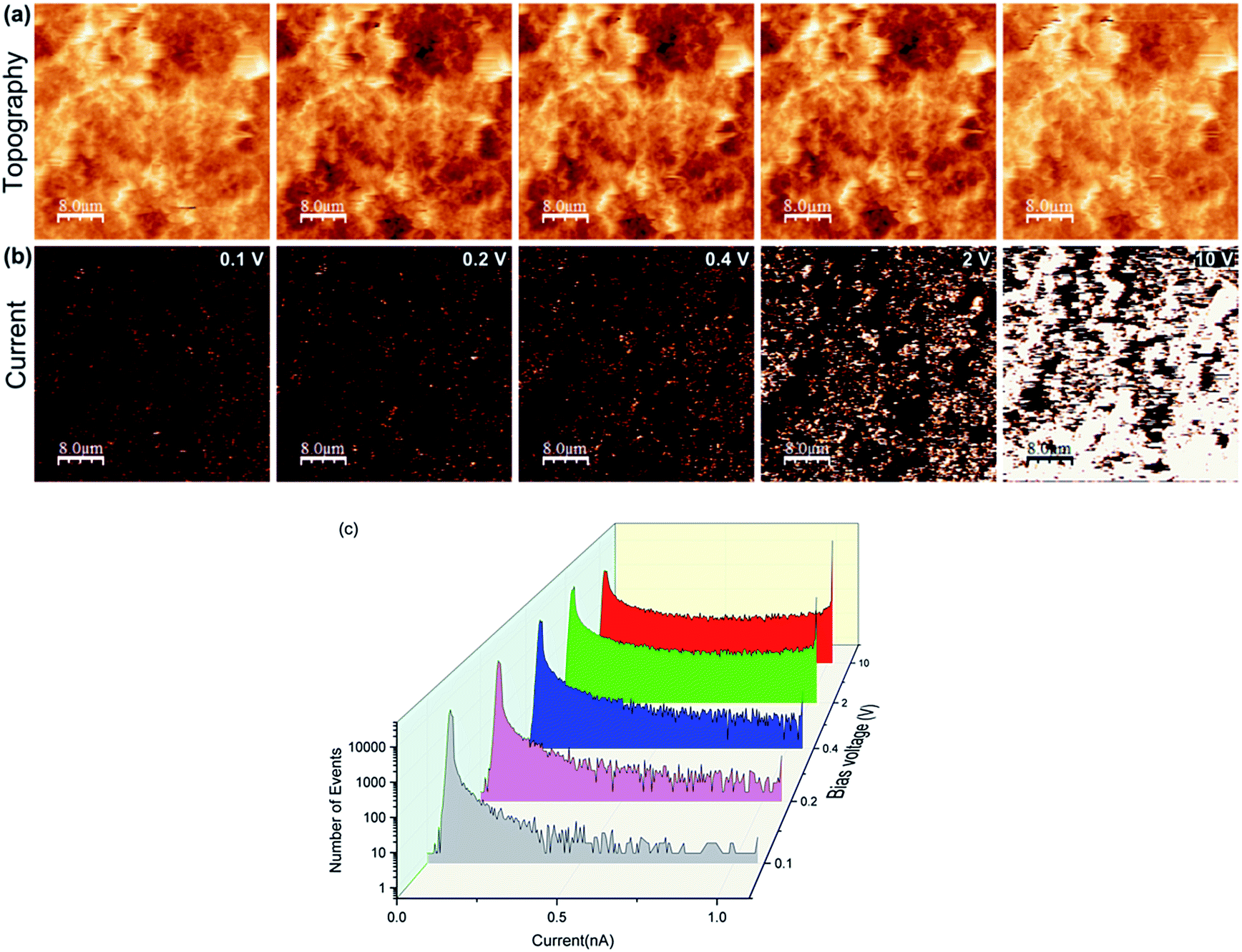 | ||
| Fig. 8 Topography (a) and current (b) from 3.5 vol% undoped CNT/PVDF sample at various bias voltages; the corresponding histograms of current (c). | ||
A closer look at the current map of Fig. 8(b) reveals that both the absolute value of the current and the number of current conducting domains increase with an increase in applied potential. These results highlight one of the powerful attributes of AFM in its ability to map the conductive domains on the surface of nanocomposite materials connected three dimensionally in through-the-thickness direction to the bottom surface in contact with the counter electrode. More importantly, in addition to the shape/size of the conductive domain, the differences in the magnitude of current flowing through different domains provide information on whether they are connected to a low resistance or high resistance percolating pathway as depicted schematically in Fig. 9.
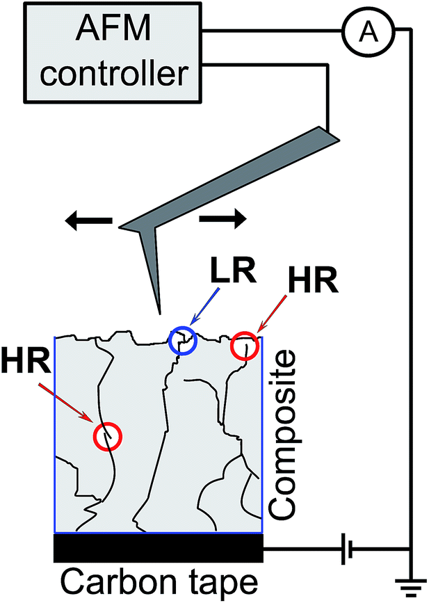 | ||
| Fig. 9 Representative low resistance (LR) and high resistance (HR) current pathways through the nanocomposite, during CS-AFM imaging. | ||
Fig. 10(a) shows the fraction of total scanned area (At) that conducts current above the threshold value. For calculating the total projected area of current per total scan area, the conducting domains were masked using a height threshold algorithm with 30 pA as threshold (∼5% total current observed, considered as noise limit).21 The percentage area of current observed per area scanned (At) for both N-doped and undoped CNT/PVDF composite samples were calculated. An increase in conducting domains with increasing potential can be noted from the figure. The steady increase in fractional conducting area with applied potential clearly indicates various resistive pathways connecting the domains. If all conductive domains on the surface were connected to the bottom electrode via a pathway with comparable resistance, then the fractional area that is conducting would not have increased although the current flowing through each domain would have increased. A spatially distributed domain with variable resistances can be extracted from the I–V measurements. However, the current saturation issue prevents a full quantitative analysis of distribution of resistance for the conductive samples. One may simplify the current domains in the CS-AFM images to low resistance path (LR) and high resistance path (HR) (Fig. 9). For 2.7 and 3.5 wt% undoped CNT and 3.5 wt% N-doped CNT composites, nearly 10% of the area contributes to current flow at 0.1 V and thus could be considered to belong to low resistance path. For 2.7 wt% N-doped CNT composite, sufficient current is observed only above 6 V and even at 10 V only 30% of the surface area appears to belong to connected network and that too to a high resistance path. Such information cannot be obtained from macroscopic conductivity experiments.
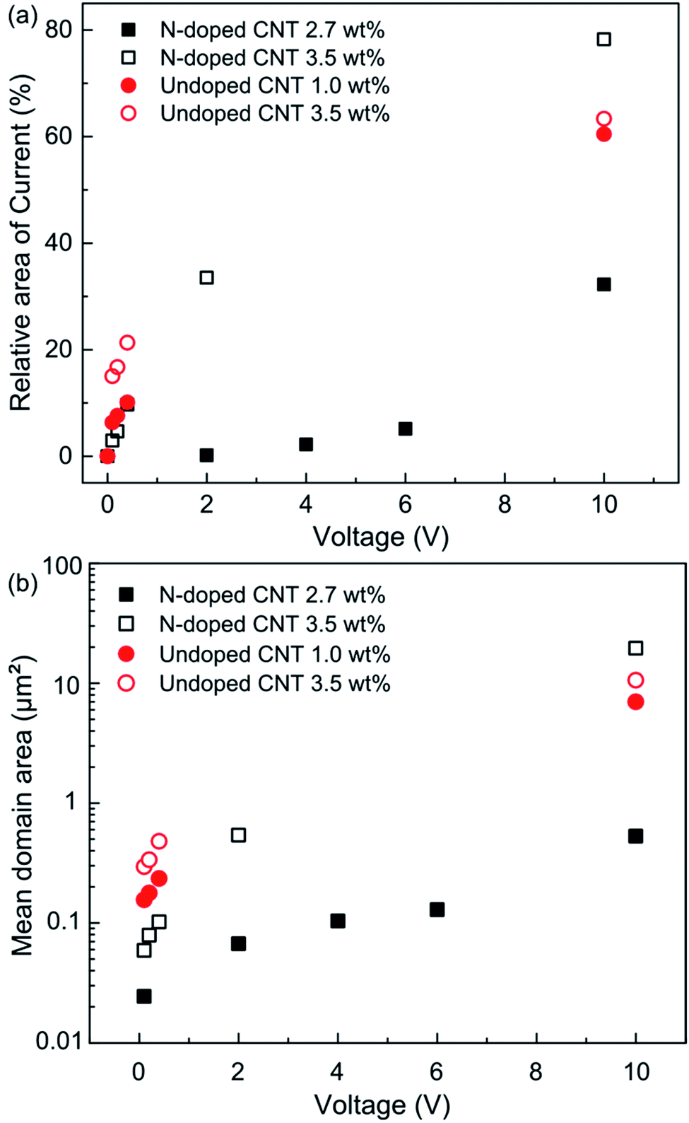 | ||
| Fig. 10 (a) The percentage area (relative) of current observed per area scanned (At) and (b) the mean domain areas calculated for both N-doped (black filled/open squares) and undoped (red filled/open circles) CNT/PVDF nanocomposite samples. Filled squares/circles contain lower wt% CNTs, while open squares/circles contain 3.5 wt% CNTs. | ||
The domain area calculated from the current micrographs is compared in Fig. 10(b). The values were obtained from the protocol adapted for calculating At. The lowest domain area measured for 2.7 wt% N-doped CNT/PVDF composite is 0.025 μm2. If the current domains are considered as circular, lowest equivalent radius can be estimated to be ∼90 nm. This is near the resolution limit due to the number of points per scan selected in this study (256 pts per line). Majority of the domains have an equivalent radius, at bias voltages below current saturation, in the range 140–400 nm. This is below the size detectable by optical microscopy and ca. 10 times bigger than the CNT diameters (Table S1†). This indicates that the percolation occurs through aggregated domains in these samples. At 10 V sample bias, the corresponding domain radii calculated was in the range 1.5–2.5 μm with the highest domain radius for 3.5 wt% N-doped CNT/PVDF sample. A dominant tunnelling mechanism instead of electron transport through connected CNTs or its aggregates should be considered at higher voltages, as suggested by Matsushige et al.10 Thus for N-doped CNT samples, a bigger domain size at 10 V bias can be attributed to the aggregates located far apart as compared to their undoped CNT equivalents. A shorter length of N-doped CNTs calculated from optical microscopy and TEM analyses support this hypothesis. In addition, the fractal analyses of the current micrographs was conducted using WSxM software's inbuilt function.26 The resulting fractal dimension values were similar for both undoped and N-doped CNT/PVDF samples. This indicates the similarity of aggregate shapes in either of the composites studied.
From the above discussed results, we tend to assign the 3D percolating network to the types shown in Fig. 3(c) or (d), an interconnected aggregate model. For N-doped CNT/PVDF samples, the connections between the aggregates will be less due to the smaller length of these CNTs.
Quantification of electrical properties from nanoscopic measurements
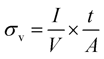
The current sensing data can be processed to obtain two key electrical properties of conductive nanocomposites: electrical conductivity and percolation threshold. In this section, we discuss our approach to quantify these two parameters. An apparent electrical conductivity can be obtained by computing the total current over the scanned area and then applying the following formula:
 | (1) |
 ; both V and I are known. Thus, the conductivity values are measured from the histogram obtained from the current images. Conductivity of the two PVDF nanocomposites calculated via this manner is presented in Fig. 11. The calculated nanoscopic conductivity values deviate from bulk conductivity values by approximately two orders of magnitude (more discussion on the bulk conductivity analysis is given in ESI†). For example, the nanoscopic conductivity value calculated for 3.5 vol% undoped CNT/PVDF sample is 0.85 S m−1 whereas the bulk conductivity value for the same sample was 69.2 S m−1. This difference can be partially attributed to the differences in the measurement techniques. Due to the current saturation in AFM current amplifier, the applied voltage in the nanoscopic measurements was kept below 0.2 V. Under these conditions, as can be noted from Fig. 10(a), only a fraction of total conductive area contributes to the measured current, mostly from the low resistance pathways. This observation is in contrast to the macroscopic conductivity measurement experiments wherein a voltage of 90 V was applied ensuring nearly all of the conductive domains contribute to the current. Trionfi et al.23 have reported such differences between CS-AFM and macroscopic conductivity measurements in an earlier study on carbon nanofiber/poly-imide composites, where they found an approximate three-order-of-magnitude discrepancy. Conductivity values were also reported to vary depending on the cantilever material.23
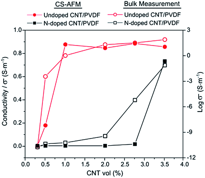 | ||
| Fig. 11 Macro and nanoscopic conductivity values of N-doped (squares) and undoped (dots) CNT/PVDF nanocomposites for different CNT concentration. Conductivity values obtained by CS-AFM method is shown in left side Y-axis (closed symbols), and that of bulk measurements in right side Y-axis (open symbols). The connecting lines are for guidance. Scan area was 40 × 40 μm2 for all samples. | ||
Percolation threshold can also be computed following the principle of Delesse,27 which allows the measured values of At to relate to the percolation probability θ∞(v) and the critical exponent β of the composites by the following equation:
 | (2) |
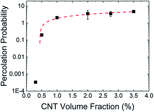 | ||
| Fig. 12 Percolation probability as a function of CNT volume fraction for the undoped CNT/PVDF composites. The red dashed line shows a power law fit following eqn (2), resulting in a critical exponent, β, of 0.53 ± 0.10. | ||
Conclusions
In this study, CS-AFM was applied to study the nanoscopic electrical properties of two CNT-based nanocomposites of PVDF. The existence of conductive domains for both undoped CNT and N-doped CNT nanocomposites was mapped as a function of applied potential. The fractional area contributing to current increased with increasing potential indicating that different conducting domains belonged to network with different resistance. The 2.7 wt% N-doped CNT composite showed few conducting domains at low voltage compared to the 3.5 wt% N-doped composite and both undoped CNT (1 wt% and 3.5%) composites; all of which showed similar response. At highest applied potential of 10 V, for 3.5 wt% undoped CNT/PVDF nanocomposite, the fractional surface area contributing to current increased from 20% at 1 V to 60% at 10 V highlighting the distinct ability to map the distribution of conducting domains with varying resistance, which is not possible with bulk conductivity measurements. This study provides direct information regarding the nanoscale percolating domains on the surface, which cannot be deduced from other microscopic techniques. The conducting domain size and fractal analyses evoke an interconnected aggregate structure of the percolating network with the low resistive conducting domain of equivalent radii ranging from 140–400 nm. Conductivity of the nanocomposites from the CS-AFM measurements were estimated but significant difference from bulk measurements was noted. This is attributed to challenges in measuring low currents at low applied potential and current saturation issues at high applied potential.Conflict of interest
The authors declare that they have no conflict of interest.Acknowledgements
We would like to thank Natural Sciences and Engineering Research Council (NSERC) of Canada. Sundararaj acknowledges funding from NSERC Discovery Grant (RGPIN/05503-2015), Canada Foundation for Innovation CFI (CFI #30100) and Alberta Advanced Education and Technology AET (AET #RCP-12-013-SEG). Karan thanks funding from NSERC Discovery Grant (RGPIN/249550-2012), Canada Foundation for Innovation CFI (CFI # 31936) and Alberta Economic Development and Trade AET (RCP-14-027-SEG). Ozhukil Kollath thankfully acknowledges University of Calgary Eyes High postdoctoral scholarship.Notes and references
- J.-M. Thomassin, C. Jérôme, T. Pardoen, C. Bailly, I. Huynen and C. Detrembleur, Mater. Sci. Eng., R, 2013, 74, 211–232 CrossRef
.
- G. Chen, W. Xu and D. Zhu, J. Mater. Chem. C, 2017, 5, 4350–4360 RSC
- Z. Zhang, G. Chen, H. Wang and X. Li, Chem.–Asian J., 2015, 10, 149–153 CrossRef CAS PubMed
- M. Moussa, M. F. El-Kady, Z. Zhao, P. Majewski and J. Ma, Nanotechnology, 2016, 27, 442001 CrossRef PubMed
- M. Moniruzzaman and K. I. Winey, Macromolecules, 2006, 39, 5194–5205 CrossRef CAS
- C.-W. Nan, Y. Shen and J. Ma, Annu. Rev. Mater. Res., 2010, 40, 131–151 CrossRef CAS
- M. Arjmand, T. Apperley, M. Okoniewski and U. Sundararaj, Carbon, 2012, 50, 5126–5134 CrossRef CAS
- M. Arjmand and U. Sundararaj, Compos. Sci. Technol., 2015, 118, 257–263 CrossRef CAS
- G. Sun, G. Chen, J. Liu, J. Yang, J. Xie, Z. Liu, R. Li and X. Li, Polymer, 2009, 50, 5787–5793 CrossRef CAS
- K. Matsushige, K. Kobayashi, N. Iwami, T. Horiuchi, E. Shitamori and M. Itoi, Thin Solid Films, 1996, 273, 128–131 CrossRef CAS
- J. Ravier, F. Houzé, F. Carmona, O. Schneegans and H. Saadaoui, Carbon, 2001, 39, 314–318 CrossRef CAS
- F. Carmona and J. Ravier, Carbon, 2002, 40, 151–156 CrossRef CAS
- F. Carmona and J. Ravier, Phys. B, 2003, 338, 247–251 CrossRef CAS
- M. J. Cadena, R. Misiego, K. C. Smith, A. Avila, B. Pipes, R. Reifenberger and A. Raman, Nanotechnology, 2013, 24, 135706 CrossRef PubMed
- S. Jafarzadeh, P. M. Claesson, P.-E. Sundell, J. Pan and E. Thormann, ACS Appl. Mater. Interfaces, 2014, 6, 19168–19175 CAS
- T. Souier, in Handbook of Research on Nanoscience, Nanotechnology, and Advanced Materials, IGI Global, 2014, pp. 343–375 Search PubMed
- M. Arjmand, K. Chizari, B. Krause, P. Pötschke and U. Sundararaj, Carbon, 2016, 98, 358–372 CrossRef CAS
- O. Breuer, U. Sundararaj and R. W. Toogood, Polym. Eng. Sci., 2004, 44, 868–879 CAS
- C. A. Schneider, W. S. Rasband and K. W. Eliceiri, Nat. Methods, 2012, 9, 671–675 CrossRef CAS PubMed
- B. Krause, R. Boldt, L. Häußler and P. Pötschke, Compos. Sci. Technol., 2015, 114, 119–125 CrossRef CAS
- D. Nečas and P. Klapetek, Open Phys., 2012, 10, 181–188 Search PubMed
- I. Horcas, R. Fernández, J. M. Gómez-Rodríguez, J. Colchero, J. Gómez-Herrero and A. M. Baro, Rev. Sci. Instrum., 2007, 78, 013705 CrossRef CAS PubMed
- A. Trionfi, D. A. Scrymgeour, J. W. P. Hsu, M. J. Arlen, D. Tomlin, J. D. Jacobs, D. H. Wang, L.-S. Tan and R. A. Vaia, J. Appl. Phys., 2008, 104, 083708 CrossRef
- D. Glennon, T. Nevell, J. Tsibouklis and R. Ewen, Mater. Res. Bull., 1998, 33, 1139–1142 CrossRef CAS
- F. Gołek, P. Mazur, Z. Ryszka and S. Zuber, Appl. Surf. Sci., 2014, 304, 11–19 CrossRef
- J. M. Gómez-Rodríguez, A. Asenjo, R. C. Salvarezza and A. M. Baró, Ultramicroscopy, 1992, 42–44, 1321–1328 CrossRef
- A. Trionfi, D. H. Wang, J. D. Jacobs, L.-S. Tan, R. A. Vaia and J. W. P. Hsu, Phys. Rev. Lett., 2009, 102, 116601 CrossRef CAS PubMed
Footnote |
| † Electronic supplementary information (ESI) available: AFM images of pure PVDF sample, extended details on physical properties of CNTs, scanning electron micrographs and bulk electrical properties of nanocomposites. See DOI: 10.1039/c7ra05640k |
| This journal is © The Royal Society of Chemistry 2017 |