 Open Access Article
Enhancing intramolecular features and identifying defects in organic and hybrid nanoarchitectures on a metal surface at room temperature using a NaCl-functionalized scanning tunneling microscopy tip
David Peyrot and
Fabien Silly *
*
CEA, IRAMIS, SPEC, TITANS, CNRS, Université Paris-Saclay, F-91191 Gif sur Yvette, France. E-mail: fabien.silly@cea.fr; Fax: +33 169088446; Tel: +33 169088019
First published on 2nd November 2017
Abstract
Scanning tunneling microscopy (STM) is a powerful method to characterize two-dimensional organic structures and their local electronic properties. Intermolecular features are usually routinely revealed using STM at very low temperature. The resolution of STM images recorded at room temperature is in comparison quite limited. We investigate here the morphology and local electronic properties of organic and hybrid nanoarchitectures laying on metal surface at room temperature using STM with a classical PtIr tip and a novel NaCl-functionalised tip. STM images show that the NaCl-functionalized tip allows revealing at room temperature intermolecular features and variation of molecular local electronic properties, that are not visible using a PtIr tip. This new method opens new opportunities for characterizing and assessing at the atomic scale the morphology and electronic properties of organic nanoarchitectures on highly conductive surfaces not only at room temperature but also at low temperature.
1 Introduction
Characterizing two-dimensional nanostructures and nanoarchitectures1–19 at the atomic scale is a challenge of nanosciences for the development of new functionalized nanomaterials for nanotechnology.20,21 Scanning probe microscopy (SPM) is a powerful technique to assess locally the topographic and electronic properties of nanostructured surfaces. During the last years intense research effort has been dedicated to improve the resolution of SPM techniques. The resolution of non-contact atomic force microscopy (nc-AFM) in vacuum at low temperature has been especially improved using functionalized SPM tips. Images of molecular carbon skeletons have been acquired at low temperature using Xe-functionalized and CO-functionalized tips.22–39 The apex of the tip is functionalized by flooding the vacuum chamber in gas when the tip temperature is below the gas condensation temperature. Gas molecules thus adsorb onto the tip apex. This technique has also been adapted to enhance the resolution of scanning tunneling microscopy (STM). Temirov et al. functionalized the STM tip apex with H2 and D2 molecules at low temperature.40 They showed that, using these tips, the STM contrast can be switched between the conventional mapping of the electronic local density of states and a new geometric imaging by selecting the appropriate tunneling bias voltage. PTCDA and tetracene molecular benzene rings appear as bright spots at low temperature in the STM images using these functionalised tips.40–42 The main drawback of these AFM and STM techniques is that they require very low temperature to first functionalised the SPM tips and then to perform the characterization of the nanostructures. To achieve atomic scale electronic contrast in the SPM images of organic nanoarchitectures, molecules often have to lay on an insulating thin film, as NaCl, to be electronically decoupled from the supporting metal surface. The challenge still consists to assess to the individual electronic properties of molecules at room temperature on metal surfaces. Intramolecular features have been observed in molecules adsorbed on metal surfaces using STM at room temperature but only using tunneling bias close to the Fermi level,43 where the integral of the density of states is close to the local density of states.44 Intermolecular features are usually lost when the tunneling bias is higher than few meV. The tunneling bias can thus not be used as a free parameter to optimize STM images, which is essential to discover new localized phenomena. Intramolecular features have been observed in molecules adsorbed on graphite,45,46 where the electronic coupling at the interface is less strong than on a metal surface.In this paper we investigate the contrast enhancement in the STM images of organic and hybrid nanoarchitectures on metal surfaces at room temperature induced by a NaCl-functionalized STM tip. Archetypal 2D model systems (PTCDI molecules47 and PTCDI–NaCl nanoarchitectures48) are selected as a benchmarks to assess the enhanced resolution of the NaCl-functionalized STM tip in comparison with a non-functionalised PtIr STM tip. STM data reveal that new electronic features appear at room temperature in the STM images recorded with the NaCl-functionalized STM tip.
2 Experimental
Experiments were performed in a ultrahigh vacuum (UHV) chamber at a pressure of 10−8 Pa. 3,4,9,10-Perylenetetracarboxylic diimide (PTCDI, C24H10N2O4) molecules (Fig. 2a) and NaCl were evaporated at 250 °C and 390 °C respectively onto a Au(111) surface. Cut PtIr tips were used to obtain constant current STM images at room temperature with a bias voltage applied to the sample. PtIr tips were cleaned and sharpen by applying pulses on the clean Au(111) surface. The PtIr tips were functionalized with NaCl by applying a bias pulse (+3 V) on top of an NaCl island. STM images were processed and analyzed using the FabViewer application.493 Results
3.1 Enhanced STM contrast in NaCl island imaging
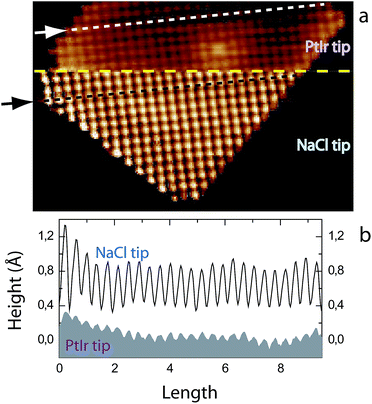
The Fig. 1a presents an STM image of a crystalline NaCl island recorded first with a sharp PtIr tip (top) and then an NaCl functionalized STM tip (bottom) at room temperature. The yellow dashed line highlights the imaging transition between the two STM tips. The STM image reveals that the resolution of the STM image is drastically improved using the NaCl-functionalized STM tip. The typical corrugation of the NaCl island taken along the line profiles indicated by the white arrow (PtIr STM tip) and the black arrow (NaCl-functionalized STM tip) is presented in Fig. 1b. The corrugation of the NaCl island is ∼0.07 Å with the PtIr STM tip, whereas its is ∼0.50 Å with the NaCl functionalized STM tip. The corrugation has been enhanced by a factor 7 using the NaCl-functionalized STM tip.3.2 Enhanced STM contrast in NaCl–PTCDI nanoarchitecture imaging
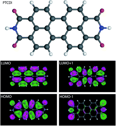
The scheme of a 3,4,9,10-perylenetetracarboxylic diimide (PTCDI) molecule and the corresponding charge density contours of LUMO, LUMO + 1, HOMO, HOMO − 1 are presented in Fig. 2. The charge density contours were calculated using complete neglect of differential overlap (CNDO) semi empirical method. This method uses two approximations: core approximation (only the outer valence electrons are explicitly included) and zero-differential overlap.50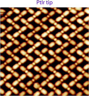 | ||
| Fig. 4 STM image of the PTCDI–NaCl mesh-nanoarchitecture48 recorded at room temperature using a clean PtIr STM tip, 14 × 14 nm2, Vs = +1.3 V, It = 180 pA. | ||
Fig. 5 shows STM images of NaCl–PTCDI “mesh”-nanoarchitecture on Au(111) recorded at room temperature using an NaCl functionalized NaCl tip. The STM images are sequentially recorded at two different tunneling bias ((a) Vs = +1.0 V and (b) Vs = −1.0 V). The STM images show that the appearance of the hybrid nanoarchitecture depends drastically of the tunneling bias.
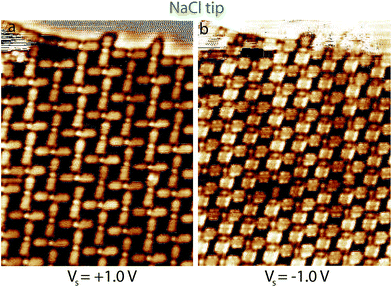 | ||
| Fig. 5 Large scale STM image of the PTCDI–NaCl mesh-nanoarchitecture at room temperature using an NaCl functionalized STM tip, 18 × 14 nm2, (a) Vs = +1.0 V, It = 365 pA; (b) Vs = −1.0 V, It = 365 pA. | ||
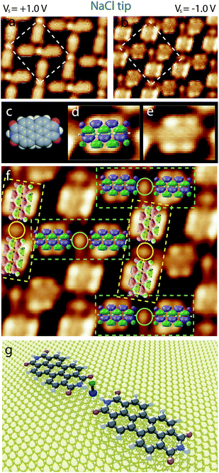
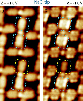
High resolution STM images of the NaCl–PTCDI “mesh”-nanoarchitecture sequentially recorded using an NaCl-functionalized tip at Vs = +1.0 V (a) and Vs = −1.0 V (b) are presented in Fig. 6. The network unit cell shape is not varying with the tunneling bias. The network unit cell of this porous structure is a rectangle with 2.3 nm and 2.5 nm unit cell constants and an angle of ∼90° between the axes (Fig. 6a and b). The STM images show that PTCDI molecules adopt a “8”-shape (LUMO + 1) for Vs = +1.0 V, whereas the molecules adopt the molecular LUMO shape for Vs = −1.0 V (see comparison between molecular skeleton, molecular LUMO and the STM image of one molecule in Fig. 6c–e). The orientation of the PTCDI molecules can be determined with a high accuracy from the high resolution STM image recorded at Vs = −1.0 V using the NaCl-functionalized tip, Fig. 6b and f. One N–H group of the PTCDI molecules is pointing toward a NaCl dimer forming straight PTCDI⋯NaCl⋯PTCDI sticks (highlighted by dashed green and yellow rectangles in Fig. 6f). A model of PTCDI⋯NaCl⋯PTCDI stick is presented in Fig. 6g. The second PTCDI N–H group is in comparison pointing toward an oxygen atom of a neighboring molecule, forming an N–H⋯O hydrogen-bond, Fig. 6f. The angle between neighboring PTCDI⋯NaCl⋯PTCDI sticks is ∼80°.
4 Discussion
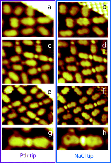
These experimental observations show that NaCl functionalized STM tip can be used to probe the local electronic properties of two-dimensional nanostructures on metal surface at room temperature. The STM images reveal that an increase of contrast (700%) has been achieved when imaging an NaCl island, Fig. 1. The NaCl-functionalized tip allows revealing at room temperature intramolecular features in organic nanoarchitectures deposited on Au(111). For example PTCDI molecules adopt a capsule-shape in the STM images recorded using a conventional PtIr tip. In contrast the molecules usually adopt a 8-shape in the STM images recorded using a NaCl-functionalized tip, Fig. 3. This 8-shape is similar to the molecular LUMO + 1 (Fig. 2). Individual molecules have a specific electronic behavior can be undoubtedly identified in the STM images recorded using the NaCl-functionalized tip. For example the PTCDI molecule in the center of the Fig. 3a has an inhomogeneous shape in the STM image recorded using the PtIr STM tip. The STM image recorded using the NaCl-functionalized tip reveals that the shape of this molecule is similar to the LUMO of the molecule, whereas the shape of the other molecules is similar to the LUMO + 1, Fig. 3b. This highlights that molecular assembly is drastically affecting the electronic properties of the molecular arrangement on metal surfaces, and this effect can be observed at room temperature using STM. High-resolution STM tips are however required to reveal this phenomenon.Additional contrast can be obtained with the NaCl STM tip by changing the tunneling bias, Fig. 6. The high resolution STM images in Fig. 6 show that the PTCDI molecules adopt the LUMO + 1 shape at Vs = +1.0 V, whereas the molecules adopt the LUMO shape at Vs = −1.0 V. The sophisticated contrast of the molecular LUMO allows precisely determining the orientation of all the PTCDI molecules in the hybrid PTCDI–NaCl nanoarchitecture. Surprisingly the molecular LUMO is observed in the STM images far from the Fermi level (Vs = −1.0 V). Cao et al. however showed that the LUMO of perylene derivatives (very similar to PTCDI molecules) is localized below the Au(111) surface Fermi level. This broad state has nevertheless a contribution close to the Fermi level.53 This explains why intramolecular details in STM images are usually observed close to the Fermi level, where the integral of the density of states is close to the local density of states.44 The appearance of the LUMO below EF is usually attributed to a more effective core hole self-screening by the excited electron in the π* molecular orbital compared to the core hole screening by metal electrons.53 Far from the Fermi level, other surface electronic contributions, such as surface states of (111) noble metal surfaces,44 are weakening the contribution of the molecules in the STM signal. It is therefore very surprising to observe intermolecular features in the STM images far from the Fermi level, especially at room temperature. Recording intermolecular features usually requires STS mapping at low temperature with the classic PtIr or W STM tip. This is one of the most interesting benefit of the NaCl functionalised STM tip. Defects in the molecular arrangement can be undoubtedly identified in these high resolution images, i.e. the shape of single molecules can differ. The STM image in Fig. 7 shows that the NaCl-functionalized tip permits to precisely identify molecules having an unusual electronic behavior.
As there is no experimental image of the tip, it is experimentally impossible to assure which NaCl species is driving the enhanced resolution of the NaCl-functionalized tip. STM images are however showing that Cl anions are appearing as a bright spots in the STM images, whereas Na cations are invisible (Fig. 1 and 5). This indicates that Cl cation density of states is having a high contrast in STM imaging. This therefore suggests that this species is most probably at the origin of the enhanced resolution of the NaCl-functionalised tip. The NaCl-functionalised STM tip was achieved numerous times using different PtIr tips, over months. Functionalizing the PtIr tip with NaCl did not appear to be more difficult than sharpening a PtIr tip with bias pulse. The NaCl functionalized-tip is able to reveal intramolecular details in the carbon skeleton of PTCDI molecules at room temperature, so this imaging method should also provide enhanced STM images of numerous carbon-based molecules, as CO-functionalized AFM tip is providing enhanced AFM images of numerous carbon-based molecules at very low temperature. The main drawn-back of this technique is that it requires depositing NaCl on the surface. NaCl self-assembles into flat crystalline islands on metal surfaces. NaCl islands have been indeed successfully grown on numerous crystalline metal surfaces, such as Cu(111),54–56 Cu(110),54,57 Cu(311),57 Ag(111),58 Ag(100),59 Ge(100),60 Al(111),61 Au(111)62 and Al(100),63 and so it is not polluting the metal surface. NaCl is however reacting with water molecules so high vacuum is required. Our experimental observations should motivate the development of detailed theoretical analysis of the use of NaCl-functionalized conductive tips in scanning tunneling microscopy as it was recently done with carbon-based tips?
5 Conclusion
To summarize, we investigated the properties of organic nanostructures on metal surface at room temperature using STM with a conventional PtIr tip and a NaCl-functionalized tip. We observed that the contrast in the STM images is greatly increased using the NaCl-functionalized tip. The NaCl-functionalized tip allows imaging at room temperature the electronic local density of states of the molecules and their precise orientation by selecting the appropriate bias tunneling voltage. The NaCl-functionalised STM tip also permits to identify local topographic and electronic defects in 2D nanoarchitectures at room temperatures. This new method opens new opportunities for characterizing and assessing at the atomic scale and at room temperature the morphology and electronic properties of organic nanoarchitectures on highly conductive surfaces. The NaCl-functionalized tip should not be limited to the STM technique but should also provide enhanced resolution in non-conductive atomic force microscopy (nc-AFM) technique. This new technique should stimulate theoretical developments to model the local electronic details observed in the STM images recorded using a NaCl-functionalized tip.Conflicts of interest
There are no conflicts to declare.Acknowledgements
The research leading to these results has received funding from the European Research Council under the European Union's Seventh Framework Programme (FP7/2007–2013)/ERC grant agreement no. 259297.References
- J. V. Barth, Annu. Rev. Phys. Chem., 2007, 58, 375–407 CrossRef CAS PubMed.
- X. Sun, F. Lafolet, G. Lemercier, F. Maurel and J.-C. Lacroix, J. Phys. Chem. C, 2017, 121, 20925–20930 CAS.
- V. Q. Nguyen, X. Sun, F. Lafolet, J.-F. Audibert, F. Miomandre, G. Lemercier, F. Loiseau and J.-C. Lacroix, J. Am. Chem. Soc., 2016, 138, 9381–9384 CrossRef CAS PubMed.
- V. A. Gorbunov, S. S. Akimenko and A. V. Myshlyavtsev, Phys. Chem. Chem. Phys., 2017, 19, 17111–17120 RSC.
- G. Pawin, K. L. Wong, K.-Y. Kwon and L. Bartels, Science, 2006, 313, 961–962 CrossRef CAS PubMed.
- S. Uemura, M. Aono, T. Komatsu and M. Kunitake, Langmuir, 2011, 27, 1336–1340 CrossRef CAS PubMed.
- T. Chen, W.-H. Yang, D. Wang and L.-J. Wan, Nat. Commun., 2013, 4, 1389 CrossRef PubMed.
- H. Liang, W. Sun, X. Jin, H. Li, J. Li, X. Hu, B. K. Teo and K. Wu, Angew. Chem., Int. Ed., 2011, 50, 7562–7566 CrossRef CAS PubMed.
- J. A. Gardener, O. Y. Shvarova, G. A. D. Briggs and M. R. Castell, J. Phys. Chem. C, 2010, 114, 5859–5866 CAS.
- L. Xu, X. Miao, B. Zha and W. Deng, Chem.–Asian J., 2013, 8, 926–933 CrossRef CAS PubMed.
- C. Tanioku, K. Matsukawa and A. Matsumoto, ACS Appl. Mater. Interfaces, 2013, 5, 940–948 CAS.
- Y. Hu, K. Miao, B. Zha, L. Xu, X. Miao and W. Deng, Phys. Chem. Chem. Phys., 2015, 18, 624–634 RSC.
- Y. Hu, K. Miao, S. Peng, B. Zha, L. Xu, X. Miao and W. Deng, CrystEngComm, 2016, 18, 3019–3032 RSC.
- Q. Shen, J. H. He, J. L. Zhang, K. Wu, G. Q. Xu, A. T. S. Wee and W. Chen, J. Chem. Phys., 2015, 142, 101902 CrossRef PubMed.
- E. Sierda, M. Abadia, J. Brede, M. Elsebach, B. Bugenhagen, M. H. Prosenc, M. Bazarnik and R. Wiesendanger, ACS Nano, 2017, 11, 9200–9206 CrossRef CAS PubMed.
- H. Y. Gao, Q. J. Shen, X. R. Zhao, X. Q. Yan, X. Pang and W. J. Jin, J. Mater. Chem., 2012, 22, 5336–5343 RSC.
- M. A. Mezour, R. M. Choueiri, O. Lukoyanova, R. B. Lennox and D. F. Perepichka, Nanoscale, 2016, 8, 16955–16962 RSC.
- J. Shang, Y. Wang, M. Chen, J. Dai, X. Zhou, J. Kuttner, G. Hilt, X. Shao, J. M. Gottfried and K. Wu, Nat. Chem., 2015, 7, 389–393 CrossRef CAS PubMed.
- D. Écija, R. Otero, L. Sánchez, J. M. Gallego, Y. Wang, M. Alcamí, F. Martín, N. Martín and R. Miranda, Angew. Chem., Int. Ed., 2007, 46, 7874–7877 CrossRef PubMed.
- S. Yagai, M. Yamauchi, A. Kobayashi, T. Karatsu, A. Kitamura, T. Ohba and Y. Kikkawa, J. Am. Chem. Soc., 2012, 134, 18205–18208 CrossRef CAS PubMed.
- S. Yagai, Bull. Chem. Soc. Jpn., 2015, 88, 28–58 CrossRef.
- S. Wickenburg, J. Lu, J. Lischner, H.-Z. Tsai, A. A. Omrani, A. Riss, C. Karrasch, A. Bradley, H. S. Jung, R. Khajeh, D. Wong, K. Watanabe, T. Taniguchi, A. Zettl, A. H. C. Neto, S. G. Louie and M. F. Crommie, Nat. Commun., 2016, 7, 13553 CrossRef CAS PubMed.
- L. Gross, F. Mohn, N. Moll, P. Liljeroth and G. Meyer, Science, 2009, 325, 1110–1114 CrossRef CAS PubMed.
- H.-Z. Tsai, A. A. Omrani, S. Coh, H. Oh, S. Wickenburg, Y.-W. Son, D. Wong, A. Riss, H. S. Jung, G. D. Nguyen, G. F. Rodgers, A. S. Aikawa, T. Taniguchi, K. Watanabe, A. Zettl, S. G. Louie, J. Lu, M. L. Cohen and M. F. Crommie, ACS Nano, 2015, 9, 12168–12173 CrossRef CAS PubMed.
- N. Moll, L. Gross, F. Mohn, A. Curioni and G. Meyer, New J. Phys., 2010, 12, 125020 CrossRef CAS.
- L. Gross, F. Mohn, N. Moll, G. Meyer, R. Ebel, W. M. Abdel-Mageed and M. Jaspars, Nat. Chem., 2010, 2, 821–825 CrossRef CAS PubMed.
- N. Pavlicek, B. Fleury, M. Neu, J. Niedenführ, C. Herranz-Lancho, M. Ruben and J. Repp, Phys. Rev. Lett., 2012, 108, 086101 CrossRef PubMed.
- L. Gross, F. Mohn, N. Moll, B. Schuler, A. Criado, E. Guitián, D. Pena, A. Gourdon and G. Meyer, Science, 2012, 337, 1326–1329 CrossRef CAS PubMed.
- D. Hayes, G. B. Griffin and G. S. Engel, Science, 2013, 340, 1431–1434 CrossRef CAS PubMed.
- S. Kawai, A. S. Foster, T. Björkman, S. Nowakowska, J. Björk, F. F. Canova, L. H. Gade, T. A. Jung and E. Meyer, Nat. Commun., 2016, 7, 11559 CrossRef CAS PubMed.
- S. P. Jarvis, Int. J. Mol. Sci., 2015, 16, 19936–19959 CrossRef CAS PubMed.
- B. Schuler, G. Meyer, D. Peña, O. C. Mullins and L. Gross, J. Am. Chem. Soc., 2015, 137, 9870–9876 CrossRef CAS PubMed.
- K. Iwata, S. Yamazaki, P. Mutombo, P. Hapala, M. Ondriek, P. Jelinek and Y. Sugimoto, Nat. Commun., 2015, 6, 7766 CrossRef CAS PubMed.
- F. Albrecht, N. Pavliček, C. Herranz-Lancho, M. Ruben and J. Repp, J. Am. Chem. Soc., 2015, 137, 7424–7428 CrossRef CAS PubMed.
- S. Kawai, A. Sadeghi, F. Xu, L. Peng, A. Orita, J. Otera, S. Goedecker and E. Meyer, ACS Nano, 2015, 9, 2574–2583 CrossRef CAS PubMed.
- M. Corso, M. Ondrácek, C. Lotze, P. Hapala, K. J. Franke, P. Jelínek and J. I. Pascual, Phys. Rev. Lett., 2015, 115, 136101 CrossRef PubMed.
- P. Hapala, M. Svec, O. Stetsovych, N. J. van der Heijden, M. Ondracek, J. van der Lit, P. Mutombo, I. Swart and P. Jelinek, Nat. Commun., 2016, 7, 11560 CrossRef CAS PubMed.
- M. Kim and J. R. Chelikowsky, Appl. Phys. Lett., 2015, 107, 163109 CrossRef.
- Z. Majzik, A. B. Cuenca, N. Pavlićek, N. Miralles, G. Meyer, L. Gross and E. Fernandez, ACS Nano, 2016, 10, 5340–5345 CrossRef CAS PubMed.
- R. Temirov, S. Soubatch, O. Neucheva, A. C. Lassise and F. S. Tautz, New J. Phys., 2008, 10, 053012 CrossRef.
- C. Weiss, C. Wagner, C. Kleimann, M. Rohlfing, F. S. Tautz and R. Temirov, Phys. Rev. Lett., 2010, 105, 086103 CrossRef CAS PubMed.
- J. I. Martínez, E. Abad, C. González, F. Flores and J. Ortega, Phys. Rev. Lett., 2012, 108, 246102 CrossRef PubMed.
- L. E. Dinca, F. De Marchi, J. M. MacLeod, J. Lipton-Duffin, R. Gatti, D. Ma, D. F. Perepichka and F. Rosei, Nanoscale, 2015, 7, 3263–3269 RSC.
- M. Pivetta, F. Silly, F. Patthey, J. P. Pelz and W.-D. Schneider, Phys. Rev. B, 2003, 67, 193402 CrossRef.
- F. Silly, J. Phys. Chem. C, 2014, 118, 11975–11979 CAS.
- W. Chen, D.-C. Qi, H. Huang, X. Gao and A. T. S. Wee, Adv. Funct. Mater., 2011, 21, 410–424 CrossRef CAS.
- M. Mura, F. Silly, G. A. D. Briggs, M. R. Castell and L. N. Kantorovich, J. Phys. Chem. C, 2009, 113, 21840–21848 CAS.
- J. Hieulle, D. Peyrot, Z. Jiang and F. Silly, Chem. Commun., 2015, 51, 13162–13165 RSC.
- F. Silly, J. Microsc., 2009, 236, 211–218 CrossRef CAS PubMed.
- J. A. Pople and D. L. Beveridge, Approximate Molecular Orbital Theory, McGraw-Hill, 1970 Search PubMed.
- A. O. Gusev, A. Taleb, F. Silly, F. Charra and M.-P. Pileni, Adv. Mater., 2000, 12, 1583–1587 CrossRef CAS.
- J. Hieulle and F. Silly, J. Mater. Chem. C, 2013, 1, 4536–4539 RSC.
- L. Cao, Y.-Z. Wang, T.-X. Chen, W.-H. Zhang, X.-J. Yu, K. Ibrahim, J.-O. Wang, H.-J. Qian, F.-Q. Xu, D.-C. Qi and A. T. S. Wee, J. Chem. Phys., 2011, 135, 174701 CrossRef PubMed.
- J. Repp, G. Meyer, F. E. Olsson and M. Persson, Science, 2004, 305, 493 CrossRef CAS PubMed.
- F. E. Olsson, S. Paavilainen, M. Persson, J. Repp and G. Meyer, Phys. Rev. Lett., 2007, 98, 176803 CrossRef.
- R. Bennewitz, A. S. Foster, L. N. Kantorovich, M. Bammerlin, C. Loppacher, S. Schär, M. Guggisberg, E. Meyer and A. L. Shluger, Phys. Rev. B: Condens. Matter Mater. Phys., 2000, 62, 2074–2084 CrossRef CAS.
- F. E. Olsson, M. Persson, A. G. Borisov, J.-P. Gauyacq, J. Lagoute and S. Fölsch, Phys. Rev. Lett., 2004, 93, 206803 CrossRef CAS PubMed.
- L. Ramoino, M. von Arx, S. Schintke, A. Baratoff, H. J. Güntherodt and T. A. Jung, Chem. Phys. Lett., 2006, 417, 22–27 CrossRef CAS.
- M. Pivetta, F. Patthey, M. Stengel, A. Baldereschi and W.-D. Schneider, Phys. Rev. B, 2005, 72, 115404 CrossRef.
- K. Glöckler, M. Sokolowski, A. Soukopp and E. Umbach, Phys. Rev. B: Condens. Matter Mater. Phys., 1996, 54, 7705–7708 CrossRef.
- W. Hebenstreit, J. Redinger, Z. Horozova, M. Schmid, R. Podloucky and P. Varga, Surf. Sci., 1999, 424, L321–L328 CrossRef CAS.
- X. Sun, M. P. Felicissimo, P. Rudolf and F. Silly, Nanotechnology, 2008, 19, 495307 CrossRef PubMed.
- W. Hebenstreit, M. Schmid, J. Redinger, R. Podloucky and P. Varga, Phys. Rev. Lett., 2000, 85, 5376–5379 CrossRef CAS PubMed.
| This journal is © The Royal Society of Chemistry 2017 |

