
 Open Access Article
 This Open Access Article is licensed under a Creative Commons Attribution-Non Commercial 3.0 Unported Licence
Investigation of Fe2+-incorporating organic–inorganic hybrid perovskites from first principles and experiments†
Long Zhou,
Jingjing Chang *,
Zhenhua Lin,
Chunfu Zhang*,
Dazheng Chen,
Jincheng Zhang and
Yue Hao*
*,
Zhenhua Lin,
Chunfu Zhang*,
Dazheng Chen,
Jincheng Zhang and
Yue Hao*
State Key Discipline Laboratory of Wide Band Gap Semiconductor Tecchnology, Shaanxi Joint Key Laboratory of Graphene, School of Microelectronics, Xidian University, 2 South Taibai Road, Xi'an, China 710071. E-mail: jjingchang@xidian.edu.cn; cfzhang@xidian.edu.cn; yhao@xidian.edu.cn
First published on 28th November 2017
Abstract
The development of high efficiency perovskite solar cells (PSCs) has been proved to depend on the stability and optical properties of perovskite materials. A lot of efforts have been applied to improving these properties. Among them, the alternative mixed-metal perovskite composition has been considered as a new solution for photovoltaic device applications to satisfy the demand for exploring efficient photovoltaic performance. Here, we have systematically performed first-principles calculations using density-functional theory (DFT) to study the structural, electronic, magnetic and optical properties of the perovskite CH3NH3(Pb:Fe)I3, and investigated the effect of iron (Fe) metal ion doping on the properties of the perovskites and solar cell performance. The calculated results reveal that the perovskite CH3NH3(Pb:Fe)I3 exhibits half-metallic behavior due to the impurity bands induced by the Fe dopant crossing the Fermi level. Consequently, it is found that the absorption intensities of CH3NH3(Pb:Fe)I3 are slightly higher than those of CH3NH3PbI3 in the near-infrared light region. It is unexpected that the perovskite CH3NH3(Pb:Fe)I3 exhibits a large magnetic moment of 4 μB and its magnetic coupling belongs to the antiferromagnetic (AFM) configuration. Meanwhile, we found that the Fe incorporation can distort the structure due to its small ionic size, which significantly changes the device performance. Our findings provide a reference for exploring the properties of perovskite materials.
Introduction
Organometallic halide perovskite materials have been considered as a new class of solution-processable direct-bandgap semiconductors for photovoltaic device applications, owing to their high light absorption coefficient, high charge carrier mobility, long charge diffusion length and low fabrication cost.1–8 In the last few years, the power conversion efficiency (PCE) of lead-based metal halide perovskite solar cells (PSCs) has rapidly risen from an initial efficiency value of 3.8%![[thin space (1/6-em)]](https://www.rsc.org/images/entities/char_2009.gif) 9 to a recent value of 22.1%10 which is much higher than those achieved by other emerging thin film solar cells11 and exceeds the threshold value for commercialization.12 One attractive feature of perovskite materials is that their properties can be modulated by composition engineering.13–16 For instance, the structure and properties of perovskites can be well tuned by using more lead compounds with different halides or non-halide anions and/or compounds with different organic cations.17,18 The band gap of perovskites can be tailored by incorporating inorganic anions like Br and Cl.19–22 One example is that the band gap of CH3NH3I3−xBrx increases with the increasing x value due to the uplift conduction band energy level, which can significantly enhance the open-circuit voltage (Voc) of the corresponding PSCs. Recently, developing lead-free devices is becoming an important topic in PSCs and it was found that the incorporation of certain polyvalent metal ions in perovskites could significantly affect their optoelectronic and crystallographic properties. For instance, the incorporation of Bi3+ into CH3NH3PbBr3 could narrow the band gap and increase the conductivity with electronic dopant,23,24 whereas alkali metal ions such as Na+ and K+ could beneficially influence the film morphology and crystallinity of CH3NH3PbI3.25 Likewise, Al3+ incorporation has been found to decrease the non-radiative recombination rate and improve crystal quality by reducing microstrain in the CH3NH3PbI3 lattice.26 Recently, Wang et al.27 demonstrated that perovskites with In3+ incorporation exhibit high film quality with multiple ordered crystal orientations which are beneficial for the efficient charge transport along multiple directions and thus improve the cells performance. Interestingly, Javier Navas et al.28 presented the synthesis of organic–inorganic hybrid perovskite CH3NH3PbI3 doped with Sn2+, Sr2+, Cd2+ and Ca2+ in the position of the Pb2+ ion and these kinds of dopants affected both the crystalline phase and the band gap energy. Therefore, it remains an attractive pursuit to identify alternative divalent metal species those are capable of both tuning the perovskite material properties and preserving the excellent photovoltaic properties.
9 to a recent value of 22.1%10 which is much higher than those achieved by other emerging thin film solar cells11 and exceeds the threshold value for commercialization.12 One attractive feature of perovskite materials is that their properties can be modulated by composition engineering.13–16 For instance, the structure and properties of perovskites can be well tuned by using more lead compounds with different halides or non-halide anions and/or compounds with different organic cations.17,18 The band gap of perovskites can be tailored by incorporating inorganic anions like Br and Cl.19–22 One example is that the band gap of CH3NH3I3−xBrx increases with the increasing x value due to the uplift conduction band energy level, which can significantly enhance the open-circuit voltage (Voc) of the corresponding PSCs. Recently, developing lead-free devices is becoming an important topic in PSCs and it was found that the incorporation of certain polyvalent metal ions in perovskites could significantly affect their optoelectronic and crystallographic properties. For instance, the incorporation of Bi3+ into CH3NH3PbBr3 could narrow the band gap and increase the conductivity with electronic dopant,23,24 whereas alkali metal ions such as Na+ and K+ could beneficially influence the film morphology and crystallinity of CH3NH3PbI3.25 Likewise, Al3+ incorporation has been found to decrease the non-radiative recombination rate and improve crystal quality by reducing microstrain in the CH3NH3PbI3 lattice.26 Recently, Wang et al.27 demonstrated that perovskites with In3+ incorporation exhibit high film quality with multiple ordered crystal orientations which are beneficial for the efficient charge transport along multiple directions and thus improve the cells performance. Interestingly, Javier Navas et al.28 presented the synthesis of organic–inorganic hybrid perovskite CH3NH3PbI3 doped with Sn2+, Sr2+, Cd2+ and Ca2+ in the position of the Pb2+ ion and these kinds of dopants affected both the crystalline phase and the band gap energy. Therefore, it remains an attractive pursuit to identify alternative divalent metal species those are capable of both tuning the perovskite material properties and preserving the excellent photovoltaic properties.
To investigate the opportunities available with alternative divalent mixed-metal perovskite composition, Sn–Pb binary metal in perovskites was applied and found that it could enlarge the material band gap by varying the Sn-to-Pb ratio.29 Klug et al.30 presented a feasibility screening study where Pb has been replaced with a second divalent metal species (Co, Cu, and Zn). It is the first systematically report that a fraction of Pb in perovskites is replaced with transition metals. Recently, Nafradi et al.31 reported the synthesis of a ferromagnetic CH3NH3(Pb:Mn)I3 photovoltaic material where photo-excited electrons rapidly melt the local magnetic order through the Ruderman–Kittel–Kasuya–Yosida interactions without heating up the spin system. The Fe is a transition metallic element which is similar to the Mn. However, the research of incorporating Fe in CH3NH3PbI3 is still not performed so far. Consequently, it is quite attractive to investigate the electronic and optical properties of Fe doped CH3NH3PbI3.
In this work, the structural, electronic, magnetic and optical properties of the perovskite CH3NH3(Pb:Fe)I3 have been systematically studied via using the first-principle calculation. The initial experiment is also carried out to investigate the effects of iron metal ions dopant on the properties of perovskites and solar cell performances. It is shown that the incorporation of Fe can affect the crystal formation, absorption and charge transport of the perovskite films. Our density functional theory (DFT) calculation results reveal that the perovskite CH3NH3(Pb:Fe)I3 exhibits a large magnetic moment of 4.0 μB and half-metallic behavior. Simultaneously, its absorption edges exhibit blue-shift relative to that of the perovskite CH3NH3PbI3. These findings demonstrate the opportunities of transition metal substitution as new dimensions for tuning the electronic and crystallographic structure properties of perovskites. Moreover, we present a kind of method to investigate the properties of halide perovskites by using GGA within DFT-vdw correction in CASTEP mode for the first time, which could provide a reference for theoretical research of the halide perovskites.
Results and discussion
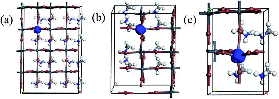
We first explored the structure properties of undoped material which has tetragonal (I4cm) crystal structure and then extended to the 2 × 1 × 2 supercell.32 The fully relaxed crystal structure is shown in Fig. 1a. Moreover, the lattice parameters, bond lengths and octahedral tilting of optimized crystal structure have been listed in Table 1. The relaxed bond lengths of Pb–I in the perovskite CH3NH3PbI3 are in the ranges of 3.15–3.24 Å, which is in good agreement with previous theoretical works.33 The value of the calculated band gap is 1.53 eV, closer to the experimental value of 1.52 eV.34 The results are similar to the ones obtained by Zhu et al.24 for the phase of CH3NH3PbI3 with tetragonal crystal symmetry. The band structure and density of states (DOS) of the perovskite CH3NH3PbI3 are calculated after structural optimization and shown in Fig. 2a and 3a, respectively. The spin-up and spin-down components of the DOS are totally symmetric, which indicates that the perovskite CH3NH3PbI3 is nonmagnetic. Moreover, it is found that the conduction bands are dominated by Pb 6p and I 5s states, whereas the valence bands are dominated by I 5p and Pb 6s states. It is notable that the bottom of the conduction band and the top of the valence band are both located at G point, indicating that the perovskite CH3NH3PbI3 is a direct band-gap material, which is important for the optical application.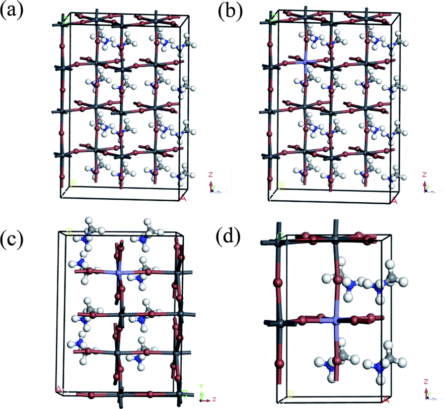 | ||
| Fig. 1 Geometric structures of the perovskite materials: (a) CH3NH3PbI3, (b) Fe doped 6.25 at%, (c) Fe doped 12.5 at%, and (d) Fe doped 25 at%. | ||
| Materials | Lattice constants | θ° | Fe–I bond (Å) | Pb–I bond (Å) | |||||
|---|---|---|---|---|---|---|---|---|---|
| a (Å) | b (Å) | c (Å) | |||||||
| Experimental values32 (CH3NH3PbI3) | 8.8929 | 8.8929 | 12.688 | 23.0 | 24.1 | 27.7 | 27.9 | — | 3.16–3.28 |
| CH3NH3PbI3 | 8.919 | 8.880 | 12.859 | 23.2 | 24.6 | 27.4 | 27.9 | — | 3.15–3.24 |
| Fe doped 6.25 at% | 8.835 | 8.8163 | 12.852 | 23.9 | 24.0 | 27.2 | 27.5 | 2.8–3.2 | 3.16–3.29 |
| Fe doped 12.5 at% | 8.785 | 8.778 | 12.892 | 22.8 | 24.7 | 27.9 | 27.2 | 2.65–3.4 | 3.15–3.41 |
| Fe doped 25 at% | 8.741 | 8.673 | 12.552 | 22.9 | 23.5 | 26.9 | 27.9 | 2.56–3.7 | 3.18–3.34 |
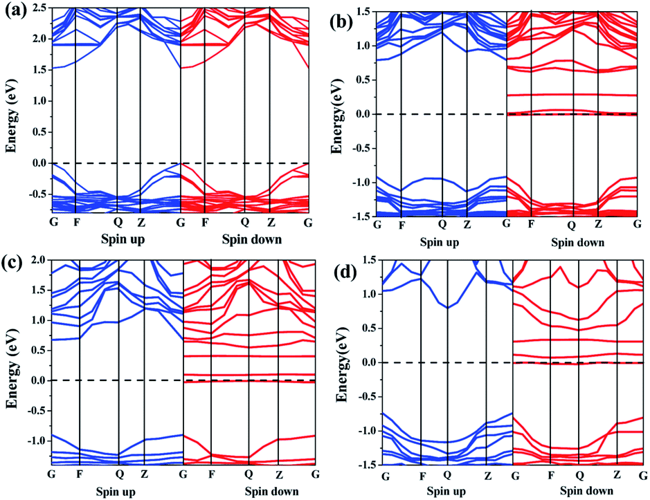 | ||
| Fig. 2 Band structures of the perovskite materials: (a) CH3NH3PbI3, (b) Fe doped 6.25 at%, (c) Fe doped 12.5 at%, and (d) Fe doped 25 at%. | ||
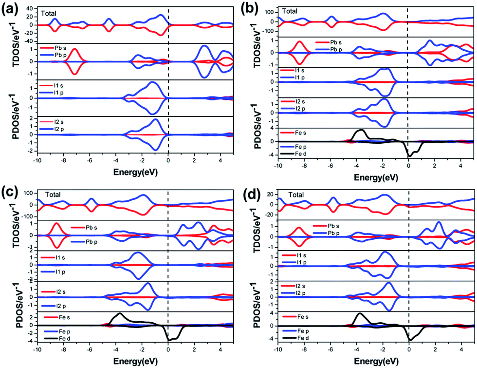 | ||
| Fig. 3 Total and partial DOS of perovskite materials: (a) CH3NH3PbI3, (b) Fe doped 6.25 at%, (c) Fe doped 12.5 at%, and (d) Fe doped 25 at%. | ||
For the perovskite CH3NH3(Pb:Fe)I3, we calculated different Fe atom doping concentrations in the crystal structure, corresponding to Fe contents of 6.25 at%, 12.5 at%, 25 at%, respectively. All atomic positions are fully relaxed after replacing the Pb atom with the Fe atom and the lattice constants of the perovskites with different concentrations are showed in Table 1. In order to investigate the effects of iron atom doping, the spin polarized band structures and corresponding partial DOS of the perovskite CH3NH3(Pb:Fe)I3 have been calculated. The spin polarized band structure of CH3NH3PbI3 has been presented in Fig. 2a. In the cases of the perovskite CH3NH3(Pb:Fe)I3 with 6.25 at%, 12.5 at%, 25 at% Fe doping concentrations, the calculated band structures are shown in Fig. 2b–d, respectively. It can be seen that the band structures of the perovskite CH3NH3(Pb:Fe)I3 with Fe atom mixed concentrations of 6.25 at% and 12.5 at% are similar to that of the perovskite CH3NH3PbI3. Both the top of valence band and the bottom of conduction band are located at the same k-point, whereas the perovskite CH3NH3(Pb:Fe)I3 with Fe concentration of 25 at% has in-direct bandgap due to the stronger interaction between atoms. Compared with the perovskite CH3NH3PbI3, the energy gap of the perovskite CH3NH3(Pb:Fe)I3 in the spin-up channel is well above 1.6 eV, whereas it should be noted that the energy gap in spin-down channel is above 0.13 eV due to impurity bands crossing the Fermi level induced by Fe dopant. These results indicate that the perovskite CH3NH3(Pb:Fe)I3 exhibits half-metallic behavior and magnetic properties. As a result, the perovskite CH3NH3(Pb:Fe)I3 is magnetic half-metallic. The half-metallic nature with a 100% spin polarization at the Fermi level is considered as a potential candidate for spintronic devices.35 More importantly, it is obvious that both the top valence bands and the bottom conduction bands are broad, indicating that these states are non-localized and the excitons can be transported to a long distance in these materials.36
To check the electronic structure in detail, we calculated the DOSs of the perovskite materials. Total and partial DOSs of the perovskite CH3NH3(Pb:Fe)I3 are presented in Fig. 3b–d. For the doped systems, it can be seen that the spin-up and spin-down DOSs are not completely symmetrical, indicating that the perovskite CH3NH3(Pb:Fe)I3 exhibits magnetic properties. It is notable that there is a clear spin polarization between the DOSs of two spin channel near the Fermi level, corresponding to the impurity band within the band structure. Moreover, it is found that the impurity band is attributed to the Fe 3d state. The conduction bands with an energy range from 0.75 eV to 4 eV are derived largely from the Pb p, Pb s and I s states. The valence bands with a range from −5 eV to −1 eV exist strong hybridization between the Pb p, I p, and Fe d states. The DOSs of from −7 eV to −9 eV are dominated by the Pb s and few I p states. The analyses of the total DOSs are well consistent with those of calculated magnetic properties. Simultaneously, partial DOS syndicate that the d electrons of the Fe atoms are responsible for the induced magnetic moments. Although Pb atoms and I atoms also exhibit spin polarization, their contribution to the magnetic moment of the doped systems is negligible.
It is noted that the perovskite CH3NH3(Pb:Fe)I3 is yet a proposed compound and so far no data on its synthesis and lattice structure are available. Generally, the structure of the perovskite materials such as CH3NH3PbI3 can be distorted when it is doped with larger or smaller ions. In order to evaluate the effect of Fe atoms doping on the crystal structure of CH3NH3PbI3, the Goldschmidt tolerance factor (t),  and octahedral factor (μ), μ = rB/rX are calculated, where rA and rB are effective ionic radii of cations and rX is the anion radius.37 The values of the tolerance factor and octahedral factor are required to be located within reasonable range and perovskite structures are stable when 0.813 ≤ t ≤ 1.107and 0.442 ≤ μ ≤ 0.895. According to this definition, the calculated values of the tolerance factor and octahedral factor are 1.036 and 0.355 for the CH3NH3FeI3, which indicates that the high incorporated concentration with Fe2+ doping can distort the perovskite crystal structure. Furthermore, with the purpose of evaluating the plausibility of the perovskite CH3NH3(Fe:Pb)I3, we calculated the formation energy of the doped systems by using the following definition:38
| ΔE = E(CH3NH3(Pb:Fe)I3) − E(CH3NH3PbI3)+μ(Pb) − μ(Fe) | (1) |
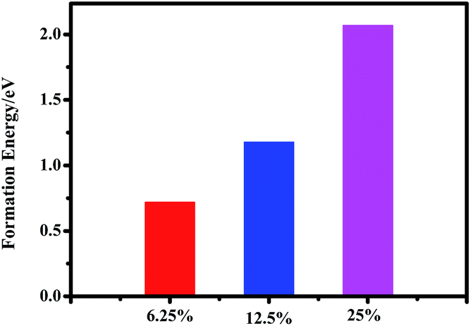 | ||
| Fig. 4 Formation energy of the perovskite CH3NH3(Fe:Pb)I3 with different incorporation. | ||
An important aspect of the perovskite CH3NH3(Pb:Fe)I3 is its magnetic behaviour. From our calculation, it is found that the total magnetic moment of the perovskite CH3NH3(Pb:Fe)I3 doped by one Fe atom is 4 μB and the magnetic properties of the systems are mainly attributed to the contribution of doped Fe impurities. Moreover, the contributions from Fe atom and its nearest-neighbouring I atoms are 3.58 μB/Fe, and 0.05 μB/I, respectively. It is clear that the spin resides mainly on the Fe atoms, and I atoms only have very minor contribution to the total magnetic moment. The magnetism distributions of the perovskite CH3NH3(Pb:Fe)I3 can be studied by the analysis of the spin density as shown in Fig. 5. It can be seen that the perovskite CH3NH3(Pb:Fe)I3 exhibits similar distribution phenomenon that magnetic moments mainly concentrate on the Fe atom, which is consistent with above calculated local magnetic moments of the Fe atom.
 | ||
| Fig. 5 Spin charge density distributions of the perovskite CH3NH3(Pb:Fe)I3: (a) Fe doped 6.25 at%, (b) Fe doped 12.5 at%, and (c) Fe doped 25 at%. | ||
To examine the type and strength of magnetic coupling between Fe dopants, we construct 2 × 1 × 2 supercell and consider four configurations of two dopant atom as shown in Fig. 6. The calculated energy differences (ΔEAFM−FM) between the antiferromagnetic (AFM) and ferromagnetic (FM) states are listed in Table 2. It is important to see that the configuration I with both Fe atoms residing at nearest-neighboring sites exhibits the lowest energy than other configurations, indicating that Fe atom has a clear clustering tendency (Fig. S1†). We found that the AFM configuration is the ground state, which is 3.1 meV lower in energy compared with the FM configuration. Negative ΔEAFM−FM values suggest that the AFM state is more favorable than the FM state. More interestingly, magnetic coupling is found to exist even if the separation distance is 12.835 Å for perovskites CH3NH3(Pb:Fe)I3, which suggests that slowly decaying extended tail of the impurity wave functions mediate the long-range magnetic coupling between local moments.39
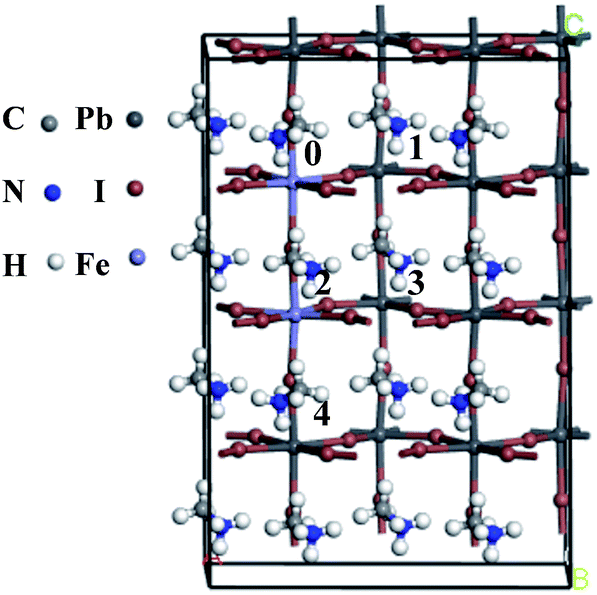 | ||
| Fig. 6 Geometric structure for 2 × 1 × 2 CH3NH3(Pb:Fe)I3 supercell. The substituted position of Fe dopants are denoted by 0–4. | ||
| Configuration | dFe-Fe (Å) | ΔEAFM−FM (meV) | Coupling | ΔEN (FM) (meV) | ΔEN (AFM) (meV) |
|---|---|---|---|---|---|
| I (0,1) | 6.407 | −3.1 | AFM | 3 | 0 |
| II (0,2) | 6.618 | −2.8 | AFM | 13 | 10 |
| III (0,3) | 8.883 | −1.6 | AFM | 50 | 48 |
| IV (0,4) | 12.835 | −0.1 | AFM | 56 | 56 |
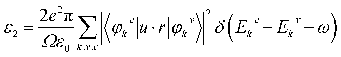
To further understand the possibilities of the CH3NH3(Pb:Fe)I3 applications in the PSCs, the optical properties are calculated. The material optical properties can be described by means of the dielectric function ε(ω) = ε1(ω) + iε2(ω), and then other properties can be expressed in terms of them. The real part ε1(ω) of the dielectric function can be calculated from the imaginary part ε2(ω) as:40
| ε1 = n2 + k2ε2 | (2) |
 | (3) |
 | (4) |
The absorption coefficients of the perovskite materials have been shown in Fig. 7. It is found that the absorption edge of the pristine CH3NH3PbI3 is above 1.5 eV, whereas that of the Fe incorporation slightly shifts to the high-energy side, which presents the blue-shift of the optical spectrum and is in good agreement with the calculated band structure. Furthermore, we found that the peak intensities of the doped systems in visible light range become weaker than those of the pristine CH3NH3PbI3, whereas the peak intensities in deep UV light region are stronger which caused by the band transitions between impurity bands and other bands. More interesting, there is a sub-gap absorption peak appears around 0.58 eV, which can be explained by the introduction of the impurity band near the Fermi level. More important, it is obviously observed that the intensities of sub-gap absorption and the main peak vary slightly with the value of U (U = 0 eV, 2.5 eV, 5 eV), as shown in Fig. S2.† Thus, the perovskite CH3NH3(Pb:Fe)I3 have enormous potential application in UV light region or infrared light region. These special properties could be considered for photodetector, particularly deep ultraviolet detector.
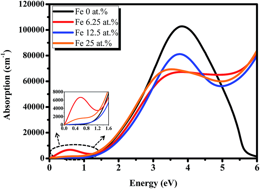 | ||
| Fig. 7 Calculated absorption coefficient of the Fe doped perovskite materials with different doping concentrations. | ||
In the calculated cases of the perovskite materials with different Fe doping concentrations, the perovskite material stability has decreased with increasing Fe concentration. Obviously, it is found that the main absorption peak with doping 12.5 at% Fe atom is the strongest for the doped systems. Thus, we have developed a perovskite CH3NH3(Pb:Fe)I3 by substituting 10% of Pb2+ with Fe2+ ions. Moreover, we fabricated devices with and without Fe doping. The PSCs architecture is similar to the previous report.42 The device without Fe dopant exhibited a Voc of 1.06 V, a short-circuit current density (Jsc) of 13.2 mA cm−2, a fill factor (FF) of 0.74, and a PCE of 10.3%. However, the incorporation of Fe2+ significantly changes the device performance. The PCE dramatically decreases to 0.9% with a Voc of 0.63 V, a Jsc of 2.7 mA cm−2, and an FF of 0.53. These results are corresponding to positive formation energy and larger octahedral factor.
The absorption spectra of the perovskite films with and without doping are shown in Fig. 8a. It is found that the perovskite film without doping exhibits strong absorption from the visible range down to the near-infrared wavelengths with the absorption onset at ca.780–785 nm that corresponds to an optical band gap of 1.58 eV, which is in good agreement with the calculated value of 1.53 eV. It is obvious that the intensities of doped system with wavelength range from 760 nm to 900 nm are stronger than those of the undoped system, which is consistent with the phenomenon in calculated absorption from 1.3 to 1.5 eV in near-infrared region. As shown in Fig. 8a, the intensities of Fe doped 10% in experimental absorption between 300 nm to 400 nm are higher than those of the undoped CH3NH3PbI3 film, which is not corresponding to the DFT calculated results with an energy range from 3.10 eV to 4.13 eV may be due to the imperfection in experiments, background (or substrate) noise, and the ideal model in calculations. Even so, it is found that the intensities of the doped system have increased in deep ultraviolet region and the tendency of absorption is in the right direction. Thus, our works could provide a reference for theoretical research of the halide perovskites.
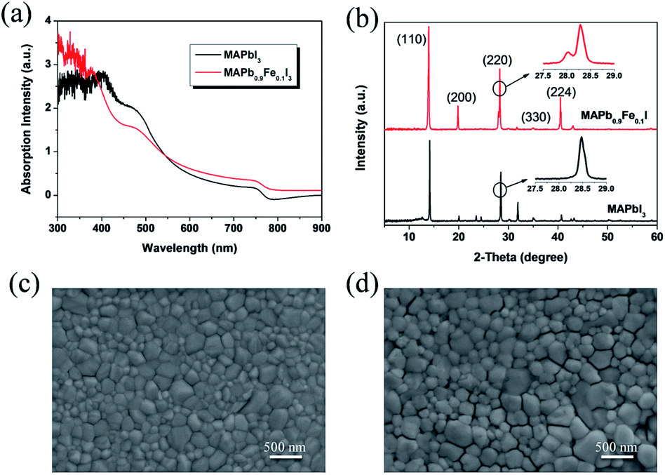 | ||
| Fig. 8 (a) UV-Vis spectra of the CH3NH3PbI3 and CH3NH3(0.9Pb:0.1Fe)I3. (b) XRD patterns of the CH3NH3PbI3 and CH3NH3(0.9Pb:0.1Fe)I3. (c and d) SEM images of the CH3NH3PbI3 (c) and CH3NH3(0.9Pb:0.1Fe)I3 (d). | ||
The structure and crystallinity of the perovskite films are more important for the PSCs, because it can affect the charge dissociation, charge transport and charge diffusion length.43 In order to further understand the effect of the iron metal ions doping on the perovskite structure and photovoltaic performance of PSCs, we investigated the structure and crystallinity of the perovskite films by XRD, as shown in Fig. 8b. The CH3NH3PbI3 films exhibit strong diffraction peaks at 14.2°, 28.5° and 31.9°. These diffraction patterns are assigned to the (110), (220) and (310) crystal planes of tetragonal perovskite, respectively. The XRD results indicate a highly crystalline nature with the (110) plane preferentially oriented. The peak positions are in good agreement with the results reported previously.43–45 For the Fe2+ doped perovskite, the intensity of the (310) peak became weak, whereas the (200) peak and the (224) peak significantly enhanced. This phenomenon suggests that the crystallinity and structure of the thin films has been changed. Furthermore, it could be seen that there are two peaks around 28.9° for the doped system in Fig. 8b, which indicates that both cubic and tetragonal crystal phase are likely present in the perovskite CH3NH3(Fe:Pb)I3 doped with 10 mol% Fe2+. The similar results have been presented by the work with the Co2+ incorporation.30
In order to further understand the effects of the iron metal ions doping on the crystal growth behaviour and photovoltaic performance of PSCs, the perovskite thin film morphology without and with iron metal ions were investigated by the field-emission scanning electron microscopy (FESEM). As shown in Fig. 8c and d, all the perovskite films whether they are doped or not are uniform with large regular crystallites, and they fully cover the underlying layer. The favourable thin film uniformity and coverage indicate a homogenous nucleation of the perovskites on the substrates. The SEM images also indicate the effect of doping the Fe2+ on the morphology of the perovskite films. Simultaneously, it is found that the large grains of micrometer can be observed when the iron metal ions doping degree is 10 mol% and the iron metal ions can promote the growth of large perovskite crystallites. Furthermore, we performed EDX elemental mapping on these thin films. As shown in Fig. S3,† the element signal at grain boundaries didn't show obvious color change, and uniform distribution. All these results indicate that Fe2+ ion is incorporated into MAPbI3 films. However, pinholes appear between the large crystallites. The pinholes can lead to large current leakage and consequently lower the PCE of PSCs. Furthermore, the iron metal ions can distort the crystal structure of the perovskite CH3NH3PbI3 due to its small ionic size. It is thus reasonable to infer that iron metal ions can change the crystallization behaviour of CH3NH3PbI3.
Conclusions
In summary, the structural, electronic, magnetic and optical properties of the perovskite CH3NH3(Pb:Fe)I3 have been systematically studied by using the first-principle calculation for the first time. We also investigated the effect of iron metal ions doping on properties of perovskites and photovoltaic performance of PSCs by experiment. Our DFT calculations reveal that the perovskite CH3NH3(Pb:Fe)I3 exhibits the large magnetic moment of 4.0 μB, which is mainly attributed to localized d states of the Fe atoms. Meantime, the AFM configuration is 3.1 meV lower in energy compared with the FM configuration, indicating that the AFM state is more favourable than the FM state. Moreover, there are impurity-bands appeared in spin-down channel crossing the Fermi level, which indicates that the doped systems exhibit half-metallic behaviour. Consequently, for the optical properties, it is found that the absorption intensities of the CH3NH3(Pb:Fe)I3 are slightly higher than the CH3NH3PbI3 in near-infrared light region and/or UV light region. Simultaneously, its absorption edges exhibit blue-shift relative to that of the perovskite CH3NH3PbI3. Despite of the results, our findings demonstrate that transition metal substitution provides new dimensions for tailoring the electronic and crystallographic properties of perovskite materials and provide a reference for exploring other efficient photovoltaic or spintronic materials and devices.Experimental
First-principles calculation
First-principles calculations are performed with the framework of density functional theory (DFT). The geometry optimization and the calculated properties have been implemented within the CASTEP code.46,47 The interaction between ions and electron is described by ultrasoft pseudo potentials. All the calculations are carried out with spin-polarizations. We use the generalized gradient approximation (GGA) with Perdew–Burke–Ernzerhof (PBE) function to explain the exchange and DFT-vdw correlations.48 A plane-wave energy cutoff of 310 eV is used throughout the calculations, which has been adopted in the previous theoretical work in similar systems. It should be noted that the convergence of total energies of the chosen plane-wave energy cutoffs is calculated to be within 10 meV even using higher energy cutoff such as 500 eV (Fig. S4†). Geometry structures are relaxed until maximum force on each structure is less than 0.03 eV Å−1, the convergence criteria for energy of 1 × 10⁻⁵ eV is satisfied, and the maximum displacement is 0.005 Å. The model of the perovskite CH3NH3(Pb:Fe)I3 is constructed starting from the experimentally determined room-temperature tetragonal (I4cm) crystal structure of undoped material, and then extended to the supercell. In the case of single doping, in order to avoid the interaction between Fe atoms, only one Fe substitution at a Pb site is considered in one supercell. Here, considering the number of the supercell, we construct three different size models of 2 × 1 × 2, 1 × 2 × 1 and 1 × 1 × 1 supercells for CH3NH3PbI3 with one Pb atom substituted by one Fe atom, as shown in Fig. 1b–d. The brillouin zone is sampled with 1 × 2 × 1, 3 × 1 × 2, 3 × 3 × 2 k-points, respectively. These models correspond to Fe mixed levels of 6.25 at%, 12.5 at%, 25 at%, respectively. The normal GGA approximation is employed although CH3NH3PbI3 was reported to have the spin-orbital coupling (SOC) effect due to the strong relativistic effect of Pb. However, it is well known that the GGA approximation underestimates the band gap,49 since it does not consider the non-continuity of the exchange-correlation. This implies that the GGA method can give accurate band gap of CH3NH3PbI3, and thus we use the generalized gradient approximation (GGA) with DFT-vdw correction to explain the exchange and correlations.50 It has been shown that GGA DFT with DFT-vdw correction is able to provide good insights into perovskite electronic structure, justifying the use of the less expensive methods for exploring novel effects. Furthermore, we also performed the calculation with DFT + U to further verify the results. The U correction is applied on d orbitals of the Fe atom. And the band structures and DOS of the doped system based on doping concentration of 12.5 at% have been shown in Fig. S5 and S6.† It could be seen that the band gap of spin down has significantly changed due to the stronger Coulomb interaction. More important, it is observed that the DFT + U only affects the conduction band and band gap.Materials and chemicals
Patterned indium tin oxide (ITO) glass substrates (10 ohm □−1) were supplied by NGS group. Poly(3,4-enthylenedioxythiophene): poly (styrence sulfonate) (PEDOT:PSS, Clevios P VP Al 4083) was purchased from Heraeus Holding GmbH. Methylammonium iodide (MAI) and [6,6]-phenyl-C61butyric acid methyl ester (PCBM) were obtained from Dyesol Ltd and Nano-C Inc., respectively. Other chemicals, including lead(II) iodide beads (PbI2, 99.999% purity), ferrous iodide (FeI2, 99.999% purity), anhydrous dimethyl sulfoxide (DMSO, ≥99.9% purity), γ-butyrolactone (GBL, ≥99% purity), LiF (≥99% purity), anhydrous chlorobenzene (99.8% purity), and anhydrous toluene (99.8% purity), were supplied by Sigma-Aldrich. All materials are used without further purification.Fabrication and characterization of PSCs
ITO glass substrates were cleaned sequentially in detergent, deionized water, acetone, and isopropanol by sonication for 20 min each. After drying under N2 stream, the substrates were further treated with UV-ozone for 15 min. A PEDOT:PSS layer with a thickness of ∼ 40 nm was prepared by spin coating clevis 4083 on ITO substrates at 8000 rpm for 1 min and subsequently annealed at 140 °C for 15 min in air. The substrates coated with PEDOT:PSS were then transferred into a glove box filled with highly pure N2. The perovskite layer was formed by spin coating a solution consisting 1.0 M (PbI2 and FeI2), and 1.0MMAIin co-solvent of DMSO:GBL (3:7 vol. ratio) at1000 rpm for 20 s, and then at 4000 rpm for 60 s. The total concentration of PbI2 and FeI2 were 1.0 M in the solutions. After 45 s from the start of the spin coating, 200 μL toluene was dripped. Then, they were annealed at 100 °C for 12 min. The thickness of the perovskite thin films was around 200 nm. The PCBM layer with a thickness of about 60 nm was deposited by spin coating a chlorobenzene solution of 20 mg mL−1 PCBM at 2000 rpm for 40 s. The devices were completed by thermally depositing LiF (0.5 nm thick) and Al (100 nm thick) in a vacuum of <1 × 10⁻⁶ Torr. Each device has an active area of 0.11 cm2. The PSCs were encapsulated with a UV-curable epoxy and cover glass slides in the glove box. The current–voltage characteristics of the PSCs were tested in air with a computer-programmed Keithley 2400 source/meter and a Newport's Oriel class A solar simulator which simulated the AM1.5 sunlight with energy density of 100 mW cm−2 and was certified to the JIS C 8912 standard. The initial scan was from −0.2 to 1.2 V.
Materials characterizations
X-ray diffraction (XRD) spectra were acquired using a BrukerD8 Advance XRD Instrument. UV-Vis Absorption spectra were recorded with a Shimadzu UV-1800 spectrophotometer. Scanning electron microscopic (SEM) images were obtained with a Zeiss Supra-40 SEM. The film thicknesses were determined using a surface profilometer (KLATencor, Alpha-Step IQ).Conflicts of interest
There are no conflicts to declare.Acknowledgements
This work was financially supported by National Natural Science Foundation of China (61604119, 61704131), Natural Science Foundation of Shaanxi Province (2017JQ6002, 2017JQ6031), Young Talent fund of China Association for Science and Technology, and the Fundamental Research Funds for the Central Universities.Notes and references
- M. M. Lee, J. Teuscher, T. Miyasaka, T. N. Murakami and H. J. Snaith, Science, 2012, 338, 643–647 CrossRef CAS PubMed.
- A. Mei, X. Li, L. Liu, Z. Ku, T. Liu, Y. Rong, M. M. Xu, M. Hu, J. Chen, Y. Yang, M. Grätzel, H. Han, M. Gratzel and H. Han, Science, 2014, 345, 295–298 CrossRef CAS PubMed.
- M. J. P. Alcocer, T. Leijtens, L. M. Herz, A. Petrozza and H. J. Snaith, Science, 2014, 342, 341–344 Search PubMed.
- H. Zhou, Q. Chen, G. Li, S. Luo, T.-b. Song, H.-S. Duan, Z. Hong, J. You, Y. Liu and Y. Yang, Science, 2014, 345, 542–546 CrossRef CAS PubMed.
- J. Burschka, N. Pellet, S.-J. Moon, R. Humphry-Baker, P. Gao, M. K. Nazeeruddin and M. Grätzel, Nature, 2013, 499, 316–320 CrossRef CAS PubMed.
- Z. Lin, J. Chang, J. Xiao, H. Zhu, Q. H. Xu, C. Zhang, J. Ouyang and Y. Hao, Sol. Energy Mater. Sol. Cells, 2016, 157, 783–790 CrossRef CAS.
- J. Chang, J. Xiao, Z. Lin, H. Zhu, Q.-H. Xu, K. Zeng, Y. Hao and J. Ouyang, J. Mater. Chem. A, 2016, 338, 643–647 Search PubMed.
- N. J. Jeon, J. H. Noh, Y. C. Kim, W. S. Yang, S. Ryu and S. Il Seok, Nat. Mater., 2014, 13, 1–7 Search PubMed.
- A. Kojima, K. Teshima, Y. Shirai and T. Miyasaka, J. Am. Chem. Soc., 2009, 131, 6050–6051 CrossRef CAS PubMed.
- National Renewable Energy Laboratories (NREL), EfficiencyChart, Rev. 01-11-2016, http://www.nrel.gov/ncpv/images/efficiency_chart.jpg.
- S. D. Stranks and H. J. Snaith, Nat. Nanotechnol., 2015, 10, 391–402 CrossRef CAS PubMed.
- W. S. Yang, J. H. Noh, N. J. Jeon, Y. C. Kim, S. Ryu, J. Seo and S. Il Seok, Science, 2015, 348, 1234 CrossRef CAS PubMed.
- H. Wang, Y. Liu, M. Li, H. Huang, H. M. Xu, R. J. Hong and H. Shen, Optoelectron. Adv. Mater., Rapid Commun., 2010, 4, 1166–1169 CAS.
- J. Chang, H. Zhu, J. Xiao, F. H. Isikgor, Z. Lin, Y. Hao, K. Zeng, Q.-H. Xu and J. Ouyang, J. Mater. Chem. A, 2016, 4, 7943–7949 CAS.
- W. Zhang, M. Saliba, D. T. Moore, S. K. Pathak, M. T. Horantner, T. Stergiopoulos, S. D. Stranks, G. E. Eperon, J. A. Alexander-Webber, A. Abate, A. Sadhanala, S. Yao, Y. Chen, R. H. Friend, L. A. Estroff, U. Wiesner and H. J. Snaith, Nat. Commun., 2015, 6, 6142 CrossRef CAS PubMed.
- N. Pellet, J. Teuscher, J. Maier and M. Gratzel, Chem. Mater., 2015, 27, 2181–2188 CrossRef CAS.
- F. K. Aldibaja, L. Badia, E. Mas-Marzá, R. S. Sánchez, E. M. Barea and I. Mora-Sero, J. Mater. Chem. A, 2015, 3, 9194–9200 CAS.
- J. H. Noh, S. H. Im, J. H. Heo, T. N. Mandal and S. Il Seok, Nano Lett., 2013, 13, 1764–1769 CrossRef CAS PubMed.
- A. Dymshits, A. Rotem and L. Etgar, J. Mater. Chem. A, 2014, 2, 20776–20781 CAS.
- J. H. Heo, D. H. Song and S. H. Im, Adv. Mater., 2014, 26, 8179–8183 CrossRef CAS PubMed.
- P. W. Liang, C. C. Chueh, X. K. Xin, F. Zuo, S. T. Williams, C. Y. Liao and A. K. Y. Jen, Adv. Energy Mater., 2015, 5, 1400960 CrossRef.
- L. Dimesso, M. Dimamay, M. Hamburger and W. Jaegermann, Chem. Mater., 2014, 26, 6762–6770 CrossRef CAS.
- A. L. Abdelhady, M. I. Saidaminov, B. Murali, V. Adinolfi, O. Voznyy, K. Katsiev, E. Alarousu, R. Comin, I. Dursun, L. Sinatra, E. H. Sargent, O. F. Mohammed and O. M. Bakr, J. Phys. Chem. Lett., 2016, 7, 295–301 CrossRef CAS PubMed.
- H. X. Zhu, J.-M. Liu, S. Kazim, M. K. Nazeeruddin, M. Grätzel, S. Ahmad, M. A. Loi, J. C. Hummelen, A. Kojima and K. Teshima, Sci. Rep., 2016, 6, 2812–2824 Search PubMed.
- J. Chang, Z. Lin, H. Zhu, F. H. Isikgor, Q.-H. Xu, C. Zhang, Y. Hao and J. Ouyang, J. Mater. Chem. A, 2016, 4, 16546–16552 CAS.
- J. T.-W. Wang, Z. Wang, S. K. Pathak, W. Zhang, D. de Quilettes, F. Wisnivesky, J. Huang, P. Nayak, J. Patel, H. Yusof, Y. Vaynzof, R. Zhu, I. Ramirez, J. Zhang, C. Ducati, C. Grovenor, M. Johnston, D. S. Ginger, R. Nicholas and H. J. Snaith, Energy Environ. Sci., 2016, 9, 2892–2901 CAS.
- Z. K. Wang, M. Li, Y. G. Yang, Y. Hu, H. Ma, X. Y. Gao and L. S. Liao, Adv. Mater., 2016, 6695–6703 CrossRef CAS PubMed.
- J. Navas, A. Sánchez-Coronilla, J. J. Gallardo, N. C. Hernández, J. C. Piñero, R. Alcántara, C. Fernández-Lorenzo, D. M. De los Santos, T. Aguilar and J. Martín-Calleja, Nanoscale, 2015, 7, 6216–6229 RSC.
- H.-J. Feng, T. R. Paudel, E. Y. Tsymbal and X. C. Zeng, J. Am. Chem. Soc., 2015, 137, 8227–8236 CrossRef CAS PubMed.
- M. T. Klug, A. Osherov, A. A. Haghighirad, S. D. Stranks, P. R. Brown, S. Bai, J. T.-W. Wang, X. Dang, V. Bulović, H. J. Snaith, A. M. Belcher, A. Kojima and K. Teshima, Energy Environ. Sci., 2017, 131, 6050–6051 Search PubMed.
- B. Náfrádi, P. Szirmai, M. Spina, H. Lee, O. V. Yazyev, A. Arakcheeva, D. Chernyshov, M. Gibert, L. Forró and E. Horváth, Nat. Commun., 2016, 7, 13406 CrossRef PubMed.
- T. Baikie, Y. Fang, J. M. Kadro, M. K. Schreyer, F. Wei, S. G. Mhaisalkar, M. Gratzel and T. White, J. Mater. Chem. A, 2013, 1, 5628–5641 CAS.
- W. Geng, L. Zhang, Y. N. Zhang, W. M. Lau and L. M. Liu, J. Phys. Chem. C, 2014, 118, 19565–19571 CAS.
- N. K. Noel, S. D. Stranks, A. Abate, C. Wehrenfennig, S. Guarnera, A.-A. Haghighirad, A. Sadhanala, G. E. Eperon, S. K. Pathak, M. B. Johnston, A. Petrozza, L. M. Herz and H. J. Snaith, Energy Environ. Sci., 2014, 7, 3061–3068 CAS.
- C. Tan, D. Sun, L. Zhou, X. Tian and Y. Huang, Superlattices Microstruct., 2016, 98, 416–422 CrossRef CAS.
- E. A. Davis and N. F. Mott, Philos. Mag., 1970, 22, 0903–0922 CrossRef CAS.
- J. Chang, Z. Lin, M. Lin, C. Zhu, J. Zhang and J. Wu, J. Mater. Chem. C, 2015, 3, 1787–1793 RSC.
- C. Freysoldt, B. Grabowski, T. Hickel, J. Neugebauer, G. Kresse, A. Janotti and C. G. Van De Walle, Rev. Mod. Phys., 2014, 86, 253–305 CrossRef.
- Y. Bai, K. Deng and E. Kan, RSC Adv., 2015, 5, 18352–18358 RSC.
- R. Chowdhury, S. Adhikari and P. Rees, Phys. B, 2010, 405, 4763–4767 CrossRef CAS.
- S. Saha, T. P. Sinha and A. Mookerjee, Phys. Rev. B, 2000, 62, 8828–8834 CrossRef CAS.
- X. Sun, C. Zhang, J. Chang, H. Yang, H. Xi, G. Lu, D. Chen, Z. Lin, X. Lu, J. Zhang and Y. Hao, Nano Energy, 2016, 28, 417–425 CrossRef CAS.
- J. Y. Jeng, Y. F. Chiang, M. H. Lee, S. R. Peng, T. F. Guo, P. Chen and T. C. Wen, Adv. Mater., 2013, 25, 3727–3732 CrossRef CAS PubMed.
- Q. Chen, H. Zhou, T. Bin Song, S. Luo, Z. Hong, H. S. Duan, L. Dou, Y. Liu and Y. Yang, Nano Lett., 2014, 14, 4158–4163 CrossRef CAS PubMed.
- J. Chang, H. Zhu, B. Li, F. Isikgor, Y. Hao, Q. Xu and J. Ouyang, J. Mater. Chem. A, 2015, 4, 887–893 Search PubMed.
- B. Delley, J. Chem. Phys., 1990, 92, 508–517 CrossRef CAS.
- B. Delley, J. Chem. Phys., 2000, 113, 7756–7764 CrossRef CAS.
- J. P. Perdew, K. Burke and M. Ernzerhof, Phys. Rev. Lett., 1996, 77, 3865–3868 CrossRef CAS PubMed.
- H. Y. Guo, Y. Zhao, N. Lu, E. Kan, X. C. Zeng, X. Wu and J. Yang, J. Phys. Chem. C, 2012, 116, 11336–11342 CAS.
- M. Dion, H. Rydberg, E. Schröder, D. C. Langreth and B. I. Lundqvist, Phys. Rev. Lett., 2004, 92, 246401 CrossRef CAS PubMed.
Footnote |
| † Electronic supplementary information (ESI) available. See DOI: 10.1039/c7ra11514h |
| This journal is © The Royal Society of Chemistry 2017 |